Analog Devices ADN2891 pra Datasheet

3.3 V 3.2 Gb/s
PRELIMINARY TECHNICAL DATA
FEATURES
SFP reference design available
Input sensitivity: 4 mV p-p
80 ps rise/fall times
CML outputs: 700 mV p-p differential
Programmable LOS detector: 3mV to 40 mV
Rx signal strength indicator (RSSI):
SFF-8472 compliant average power measurement
Single-supply operation: 3.3 V
Low power dissipation: 145 mW
Available in space-saving 3 mm × 3 mm 16-lead LFCSP
Extended Temperature Range: -40
APPLICATIONS
SFP/SFF/GBIC optical transceivers
OC-3/12/48, GbE, Fibre Channel receivers
10GBASE-LX4 transceivers
WDM transponders
o
C to 95oC
Limiting Amplifier
ADN2891
GENERAL DESCRIPTION
The ADN2891 limiting amplifier works as a data quantizer
optimized for SONET, Gigabit Ethernet (GbE), and Fibre
Channel optical receivers in the range of 155Mpbs and up to
3.2Gbps . It accepts input levels of up to 2.0 V p-p differential
with 4mV p-p differential input sensitivity and outputs current
mode logic (CML) voltages with controlled edge speeds..
The ADN2891 measures average received power based on a
direct measurement of the photodiode current with better than
1 dB of accuracy over the entire input range of the receiver. This
eliminates the need for external RSSI detection circuitry in SFF8472 compliant optical transceivers.
Additional features includes a programmable loss-of-signal
(LOS) detect and output Squelch.
The ADN2891 limiting amplifier operates from a single 3.3 V
supply, has low power dissipation, and is available in a 3 mm × 3
mm 16-lead lead frame chip scale package (LFCSP).
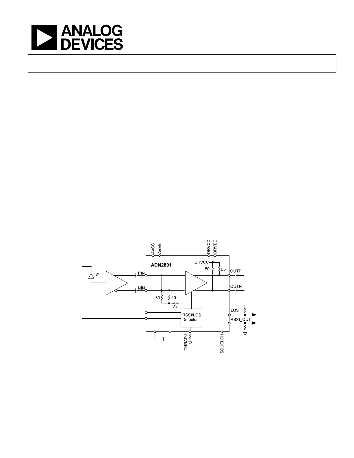
FUNCTIONAL BLOCK DIAGRAM
ADN2880
PD_VCC
PD_CATHODE
C
AZ1
µ
F
0.01
Figure 1. ADN2891 Typical Application Circuit
Rev. PrA.
Information furnished by Analog Devices is believed to be accurate and reliable.
However, no responsibility is assumed by Analog Devices for its use, nor for any
infringements of patents or other rights of third parties that may result from its use.
Specifications subject to change without notice. No license is granted by implication
or otherwise under any patent or patent rights of Analog Devices. Trademarks and
registered trademarks are the property of their respective owners.
V
REF
C
AZ2
+V
10kΩ
ADuC7020
One Technology Way, P.O. Box 9106, Norwood, MA 02062-9106, U.S.A.
Tel: 781.329.4700
Fax: 781.326.8703 © 2004 Analog Devices, Inc. All rights reserved.
www.analog.com

ADN2891 PRELIMINARY TECHNICAL DATA
TABLE OF CONTENTS
Specifications..................................................................................... 3
Loss of Signal (LOS) Detector .....................................................8
Absolute Maximum Ratings............................................................ 5
Thermal Resistance ...................................................................... 5
ESD Caution.................................................................................. 5
Pin Configuration and Function Descriptions............................. 6
Typical Performance Characteristics ............................................. 7
Theory of Operation ........................................................................ 8
LIMAMP ....................................................................................... 8
REVISION HISTORY
Revision PrA: Initial Version
Received Signal Strength Indicator (RSSI) ................................8
Squelch Mode ................................................................................8
Applications Information .................................................................9
PCB Design Guidelines ................................................................9
Outline Dimensions ....................................................................... 11
Ordering Guide .......................................................................... 11
Rev. PrA | Page 2 of 12

PRELIMINARY TECHNICAL DATA ADN2891
SPECIFICATIONS
Table 1. Test Conditions: VCC = 3.0V to 3.6V, VEE = 0 V, TA = -40 oC to 95 oC, unless otherwise noted.
Parameter Min Typ Max Unit Test Conditions/Comments
QUANTIZER DC CHARACTERISTICS
Input Voltage Range 1.8 2.8 V p-p @ PIN or NIN, dc-coupled
Input Common Mode 2.1 2.7 V DC-coupled
Peak-to-Peak Differential Input Range 2.0 V p-p PIN − NIN, ac-coupled
Input Sensitivity 4 3 mV p-p
PIN − NIN, BER ≤ 1 × 10
Input Offset Voltage 100 µV
Input RMS Noise 205 µV rms
Input Resistance 50 Ω Single-ended
Input Capacitance 0.65 pF
QUANTIZER AC CHARACTERISTICS
Input Data Rate 155 3200 Mb/s
Small Signal Gain 51 dB Differential
S11 −10 dB Differential, f < 3.2 GHz
S22 −10 dB Differential, f < 3.2 GHz
Random Jitter 2.4 5 ps rms
Deterministic Jitter 13.7 19 ps p-p
Input > 10 mV p-p, OC-48, PRBS 2
Input > 10 mV p-p, OC-48, PRBS 2
Low Frequency Cutoff 30 kHz CAZ = Open
1.0 kHz CAZ = 0.0 1 µF
Power Supply Rejection 45 dB 100 kHz < f < 10 MHz
LOSS OF SIGNAL DETECTOR (LOS)
LOS Assert Level TBD 2.0 TBD mV p-p R
TBD 40 TBD mV p-p R
Hysteresis 3.0 TBD dB
TBD 3.0 dB
4.5 TBD dB
TBD 4.5 dB
= 1MΩ
THRADJ
= 500 Ω
THRADJ
OC-3, PRBS 2
OC-3, PRBS 2
OC-48, PRBS 2
OC-48, PRBS 2
23
23
− 1, R
− 1, R
23
− 1, R
23
− 1, R
LOS Assert Time 600 ns DC-coupled
LOS De-Assert Time 100 ns DC-coupled
RSSI
Input Current Range 5 1000 µA
RSSI Output Accuracy 15%
I
≤ 20 µA
IN
10% IIN > 20 µA
Gain 1.0 mA/mA I
RSSI/IPD
Offset 50 nA
Compliance Voltage VCC − 0.9 VCC − 0.3 V @ PD_CATHODE
POWER SUPPLIES
V
CC
I
CC
OPERATING TEMPERATURE RANGE −40 +25 +95 °C T
3.0 3.3 3.6 V
44 60 mA
to T
MIN
MAX
CML OUTPUT CHARACTERISTICS
Output Impedance 50 Ω Single-ended
Output Voltage Swing 600 700 800 V p-p Differential
Output Rise and Fall Time 80 100 ps 20% to 80%
LOGIC INPUTS (SQUELCH)
VIH, Input High Voltage 2.0 V
VIL, Input Low Voltage 0.8 V
Input Current −100 nA I
100 nA I
, VIN = 2.4 V
INH
, VIN = 0.4 V
INL
THRADJ
THRADJ
THRADJ
THRADJ
−10
= 500 Ω
= 1MΩ
= 500 Ω
= 1M Ω
23
− 1
23
− 1
Rev. PrA | Page 3 of 12

ADN2891 PRELIMINARY TECHNICAL DATA
Parameter Min Typ Max Unit Test Conditions/Comments
LOGIC OUTPUTS (LOS)
VOH, Output High Voltage 2.4 V
VOL, Output Low Voltage 0.4 V
Open drain output, 4.7 kΩ − 10 kΩ
pull-up resistor to V
CC
Open drain output, 4.7 kΩ − 10 kΩ
pull-up resistor to V
CC
Rev. PrA | Page 4 of 12
 Loading...