

3.2 Gbps, 3.3 V, Low Noise,
FEATURES
Bandwidth: 2.5 GHz
Optical sensitivity: −24.2 dBm
Differential transimpedance: 4400 V/A
Power dissipation: 70 mW
Differential output swing: 260 mV p-p
Input overload current: 4.3 mA p-p
On-chip RSSI function
Low frequency cutoff: 20 kHz
On-chip PD filter: R
= 200 Ω, CF = 20 pF
F
Die size: 0.7 mm × 1.2 mm
APPLICATIONS
3.2 Gbps or below optical receivers
SONET/GbE/FC optical receivers
SFF-8472-compliant receivers
PIN/APD-TIA receive optical subassemblies (ROSA)
1
Transimpedance Amplifier
ADN2880
GENERAL DESCRIPTION
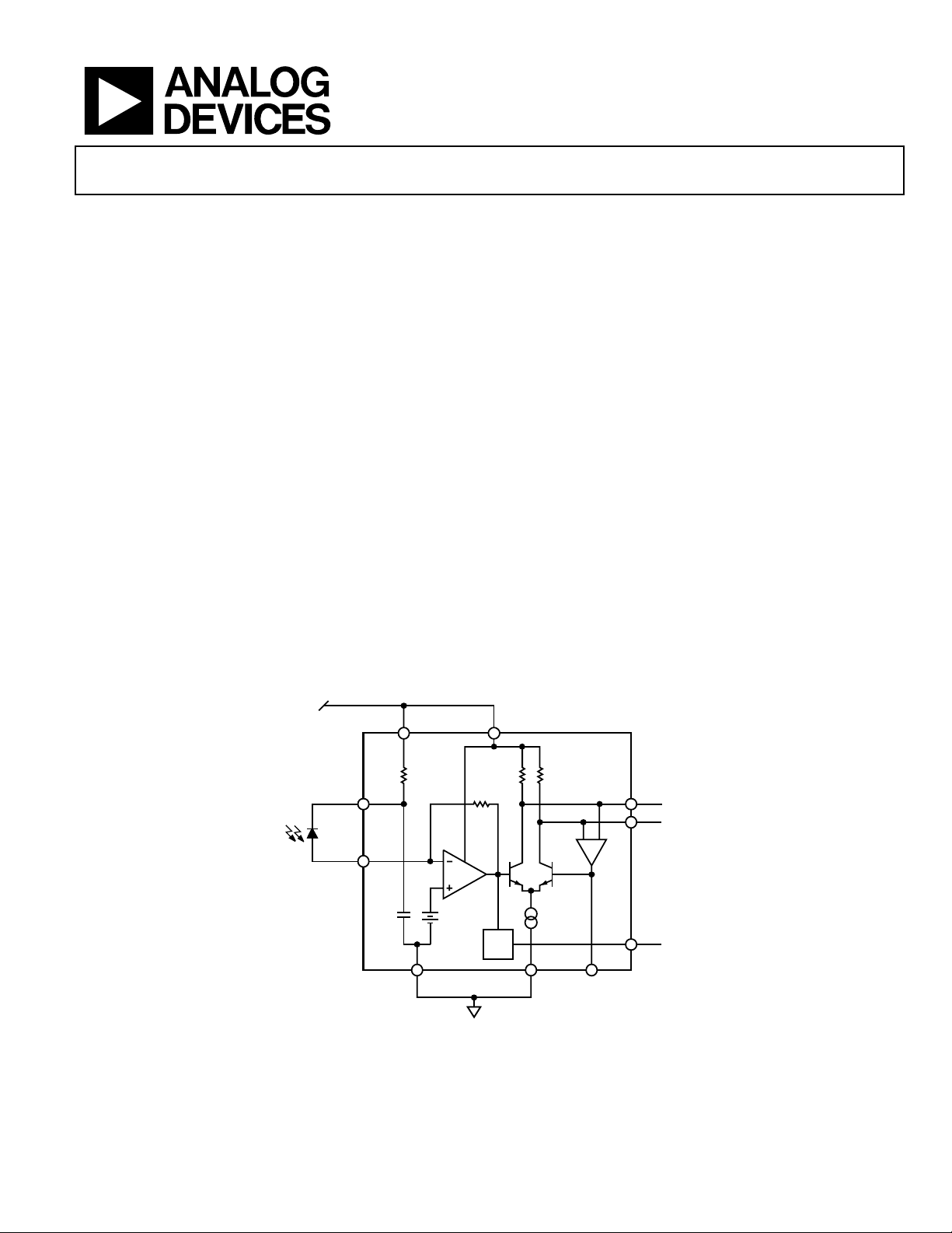
The ADN2880 is a 3.3 V, high gain SiGe transimpedance
amplifier (TIA). The TIA converts the small signal current of a
photo detector into differential voltage output. The ADN2880
features a 315 nA typical input-referred noise, enabling an
optical sensitivity of −24.2 dBm (0.85 A/W PIN). With a
bandwidth of 2.5 GHz, the ADN2880 allows a data rate
operation up to 3.2 Gbps. Typical power dissipation is
approximately 70 mW.
To facilitate the assembly in small form factor packages, such
as TO-46 headers, the ADN2880 provides an on-chip RC filter
(200 Ω, 20 pF) and features a 20 kHz low frequency cutoff
without using an external capacitor. An on-chip RSSI circuit,
which generates a voltage proportional to the average photodiode current, is also available for power monitoring and
assembly alignment.
The ADN2880 is available in die form. With a chip area of
1.2 mm × 0.7 mm, the TIA layout is specifically optimized for
TO-Can-based packages.
1
Based on 1550 nm PIN, responsivity = 0.85 A/W, ER = 9 dB, BER < 10
−10
.
FUNCTIONAL BLOCK DIAGRAM
3.3V
VCCFILTER VCC
FILTER
IN
20pF
Rev. 0
Information furnished by Analog Devices is believed to be accurate and reliable. However, no
responsibility is assumed by Anal og Devices for its use, nor for any infringements of patents or ot her
rights of third parties that may result from its use. Specifications subject to change without notice. No
license is granted by implication or otherwise under any patent or patent rights of Analog Devices.
Trademarks and registered trademarks are the property of their respective owners.
0.85V
GND GND CAP
50Ω200Ω 50Ω
1400Ω
Figure 1.
OUT
OUTB
5mA
RSSI
04945-001
One Technology Way, P.O. Box 9106, Norwood, MA 02062-9106, U.S.A.
Tel: 781.329.4700 www.analog.com
Fax: 781.461.3113 © 2005 Analog Devices, Inc. All rights reserved.

ADN2880
TABLE OF CONTENTS
Features .............................................................................................. 1
Pad Layout and Function Descriptions..........................................5
Applications....................................................................................... 1
General Description ......................................................................... 1
Functional Block Diagram .............................................................. 1
Revision History ............................................................................... 2
Electrical Specifications................................................................... 3
Absolute Maximum Ratings............................................................ 4
ESD Caution.................................................................................. 4
REVISION HISTORY
7/05—Revision 0: Initial Version
Typical Perform anc e Characte ristics ..............................................6
Assembly Recommendations...........................................................9
Outline Dimensions ....................................................................... 12
Die Information.......................................................................... 12
Ordering Guide .......................................................................... 12
Rev. 0 | Page 2 of 12

ADN2880
ELECTRICAL SPECIFICATIONS
Minimum/maximum VCC = 3.3 V ± 0.3 V, T
Table 1.
Parameter Conditions Min Typ Max Unit
DYNAMIC PERFORMANCE
Bandwidth (BW)
Total Input Referred RMS Noise (I
Total Input Referred RMS Noise (I
Small Signal Transimpedance (ZT)
1
RMS
RMS
1
−3 dB 1.9 2.5 GHz
) CD = 0.8 pF, dc to 2.1 GHz 315 485 nA
) CD = 0.6 pF, dc to 2.1 GHz 300 nA
100 MHz, differential 2700 4400 6200 V/A
100 MHz, single-ended 1350 2200 3100 V/A
Low Frequency Cutoff CAP = open, IIN = 20 μA 20 kHz
CAP = 1 nF, IIN = 20 μA 1.0 kHz
Output Return Loss DC to 3.5 GHz, differential −26 −20 dB
Input Overload Current ER = 10 dB, at 95°C
Maximum Differential Output Swing I
Output Data Transition Time I
PSRR IIN = 0 mA, <10 MHz 39 dB
Group Delay Variation 1.0 GHz to 3.0 GHz 50 ps
Transimpedance Ripple 50 MHz to 1.0 GHz, single-ended 0.93 dB
Deterministic Jitter 10 μA < I
100 μA < I
10 μA < I
Linear Output Range Differential, <1 dB compression 210 mV p-p
Linear Input Current Range Single-ended, <1 dB compression 53 μA p-p
DC PERFORMANCE
Power Dissipation I
Input Voltage Compliance voltage 0.85 V
Output Common-Mode Voltage DC (50 Ω) terminated to VCC VCC − 0.12 V
Output Impedance Single-ended 50 Ω
PD FILTER Resistance R
PD FILTER Capacitance CF 20 pF
RSSI Gain I
RSSI Offset I
RSSI Accuracy 5 μA < I
20 μA < I
1
An equivalent I
= 13 μA current signal is applied to the TIA input. No input capacitor is applied.
IN, P-P
= −40°C to +95°C; typical VCC = 3.3 V, T
AMBIENT
1
= 2.0 mA 170 260 375 mV p-p
IN, P- P
= 1.0 mA; 20% to 80% rise/fall time 60 ps
IN, P-P
≤ 100 μA, K28.5 @ 3.2 Gbps 16 ps p-p
IN, P- P
≤ 2.0 mA, K28.5 @ 3.2 Gbps 25 ps p-p
IN, P- P
≤ 2.0 mA, PRBS 231 − 1 at OC48 (FEC) 38 ps p-p
IN, P- P
= 0 mA 70 110 mW
IN, AVE
F
= 5 μA to 1 mA 0.85 V/mA
IN, AVE
= 10 μA 8.0 mV
IN, AVE
≤ 20 μA ±7 %
IN, P- P
≤ 1 mA ±3 %
IN, P- P
= 25°C, unless otherwise noted.
AMBIENT
1
2.1
4.3 mA p-p
200 Ω
Rev. 0 | Page 3 of 12
ADN2880
ABSOLUTE MAXIMUM RATINGS
Table 2.
Parameter Rating
Supply Voltage (VCC to GND) 5 V
Maximum Voltage to All Input
and Output Signal Pins
Minimum Voltage to All Input
and Output Signal Pins
Maximum Input Current 10 mA
Storage Temperature Range −65°C to +125°C
Operating Ambient Temperature Range −40°C to +95°C
Maximum Junction Temperature 125°C
Die Attach Temperature (<30 sec) 410°C
VCC + 0.4 V
GND – 0.4 V
Stresses above those listed under Absolute Maximum Rating
may cause permanent damage to the device. This is a stress
rating only; functional operation of the device at these or any
other conditions above those indicated in the operational
section of this specification is not implied. Exposure to absolute
maximum rating conditions for extended periods may affect
device reliability.
ESD CAUTION
ESD (electrostatic discharge) sensitive device. Electrostatic charges as high as 4000 V readily accumulate on the
human body and test equipment and can discharge without detection. Although this product features
proprietary ESD protection circuitry, permanent damage may occur on devices subjected to high energy
electrostatic discharges. Therefore, proper ESD precautions are recommended to avoid performance
degradation or loss of functionality.
Rev. 0 | Page 4 of 12

ADN2880
R
R
PAD LAYOUT AND FUNCTION DESCRIPTIONS
VCC VCC VCCFILTER GND
TEST
FILTE
FILTE
1 1314151617GND
IN
2
3
4
5 678 9
GNDCAPRSSIGND
Figure 2. Pad Layout
12
11
10
GND
OUT
OUTB
GND
04945-002
Table 3. Pad Function Descriptions
Pad No. Mnemonic Pin Type1Description
1 GND P Ground. (Input return.)
2 IN AI Current Input. Bond directly to a photodiode (PD) anode.
3 TEST AI Test Probe Pad. Do not connect.
4, 5 FILTER AO Filter Output. Pad 4 and Pad 5 are metal connected. Optional bond to a PD cathode.
6 GND P Ground.
7 RSSI AO Voltage Output. Provides average input current monitoring. If not used, connect to ground.
8 CAP AI
Low Frequency Cutoff (LFC) Setpoint. For SONET applications, see
Figure 10 and contact sales
for assembly details.
9, 10, 13, 14 GND P Ground. (Output return.)
11 OUTB AO Negative Output, CML, On-Chip 50 Ω Termination (AC or DC Termination).
12 OUT AO Positive Output, CML, On-Chip 50 Ω Termination (AC or DC Termination).
15 VCCFILTER P
On-Chip Filter Supply. Connect to VCC to Enable On-Chip RC Filter (200 Ω, 20 pF). Leave
unconnected if not used.
16, 17 VCC P
3.3 V Supply. Place a 200 pF, RF decoupling capacitor close to the power pad to reduce
the power noise.
1
P = power; AI = analog input; and AO = analog output.
Rev. 0 | Page 5 of 12

ADN2880
TYPICAL PERFORMANCE CHARACTERISTICS
70
65
60
55
50
45
(dB-Ω)
Z
T
40
35
30
25
FREQUENCY (Hz)
Q OUTPUT
Figure 3. Single-Ended Transimpedance vs. Frequency
5.0
QB OUTPUT
100G10M 100M 1G 10G
04945-017
3.2
3.0
2.8
2.6
2.4
BANDWIDTH (GHz)
2.2
2.0
3.6V
TEMPERATURE (°C)
3.3V
3.0V
100–40 0 40 80–20 20 60
04945-019
Figure 6. Bandwidth vs. VCC and Temperature
90
4.8
4.6
4.4
(kΩ)
Z
T
4.2
4.0
3.8
3.6V
3.0V
TEMPERATURE (°C)
Figure 4. Differential Transimpedance vs. VCC and Temperature
5.5
5.0
4.5
4.0
(kΩ)
Z
3.5
T
3.0
3.3V
85
80
75
70
65
60
POWER DISSIPATION (mW)
55
100–40–200 20406080
04945-018
50
3.6V
3.3V
3.0V
TEMPERATURE (°C)
100–40 0 40 80–20 20 60
04945-020
Figure 7. Power Dissipation vs. VCC and Temperature
–20
–25
–30
–35
SDD22
–40
2.5
2.0
I
(μA)
INPP
Figure 5. Differential Transimpedance vs. Input Current
1000 102030 506040 70 80 90
04945-027
Rev. 0 | Page 6 of 12
–45
–50
FREQUENCY (Hz)
Figure 8. SDD22 vs. Frequency up to 3.5 GHz, CAP = Open
4G10M 100M 1G
04945-021

ADN2880
1,000
3.0
2.5
100
10
LOW FREQUENCY CUTOFF (kHz)
1
INPUT CURRENT (μA)
CAP = 1nF
Figure 9. Low Frequency Cutoff vs. Input Current
18
16
14
12
10
8
6
4
LOW FREQUENCY CUTOFF (kHz)
2
0
EXTERNAL CAPACITANCE AT CAP (pF)
Figure 10. Low Frequency Cutoff vs. Capacitance at CAP
30
CAP = OPEN
2.0
(V)
1.5
RSSI
V
1.0
0.5
1,00010 100
04945-007
0
IIN (mA)
501234
04945-008
Figure 12. Full-Scale of RSSI Voltage Output vs. Input Current
350
350
340
330
320
310
300
NOISE (nA)
290
RMS
I
280
270
260
10,0001 10 100 1,000
04945-031
250
TEMPERATURE (°C)
95–40 –10–25 205 35506580
04945-028
Figure 13. Input Noise vs. Temperature with 2 GHz Low-Pass Filter
350
25
20
15
(mV)
RSSI
V
10
5
0
IIN (μA)
Figure 11. RSSI Voltage Output vs. Input Current (0 μA to 35 μA)
3505 1510 20 25 30
04945-024
Rev. 0 | Page 7 of 12
325
300
275
INPUT REFERRED RMS NOISE (nA)
250
PHOTODIODE CAPACITANCE (pF)
1.00 0.2 0.4 0.6 0.8
04945-048
Figure 14. Input Referred Noise (DC to 2.0 GHz) vs.
Photodiode Capacitance C
(pF)
D

ADN2880
5.5
5.0
4.5
5.0mV/DIV
52.9ps/DIV
OPTICAL POWER –22.7dBm
Figure 15. Output Eye at 3.2 Gbps with BER <10
Responsivity = 0.91 A/W, ER = 9 dB, PRBS 2
50
25
0
GROUP DELAY (ps)
–25
–50
FREQUENCY (GHz)
Figure 16. Group Delay vs. Frequency
−10
(Based on a 1550 nm PIN,
31
)
4.0
3.5
INPUT OVERLOAD CURRENT (mA p-p)
3.0
04945-011
TEMPERATURE (°C)
95–40 –10 5–25 2035506580
04945-030
Figure 17. Input Overload Current vs. Temperature
40123
04945-010
Rev. 0 | Page 8 of 12

ADN2880
ASSEMBLY RECOMMENDATIONS
Coplanar PIN Photodiode for SDH/SONET
Dual Planar PIN/APD Photodiode for SDH/SONET
VPD
C
PD
C
A
OUTB
Figure 18. 5-Pin TO-46 with External Photodiode Supply V
Connected Through the FILTER Pin
B.W B.W.
V
CC
C
B
B.W. B.W.
V
PD
C
PD
B.W.
FILTER
B.W.
IN
VCC
50Ω200Ω 50Ω
0.85V20pF
VCC
C
OUT
VPD
C
PD
C
B
04945-042
PD
Figure 20. 5-Pin TO-46 with External Photodiode Supply V
A
OUTB
PD
VCC
C
OUT
B
04945-049
to
PD
a Dual Planar PIN or APD
B.W B.W.
V
CC
0.85V20pF
VCC
50Ω200Ω 50Ω
B.W.
B.W.
RSSI
OUT
OUTB
B.W.
B.W.
RSSI
OUT
OUTB
C
B
B.W.
V
PD
C
PD
B.W.
IN
GND GND CAP
B.W. B.W.
B.W.
Figure 19. Equivalent Circuit of the Assembly Including Bond Wires
Table 4. Bill of Materials (BOM)
Component Description
PD 1× vendor specific, 2.5 Gbps, photodiode
TIA
1× ADN2880 (0.7 mm × 1.2 mm), 3.2 Gbps,
transimpedance amplifier
C
B
C
PD
C
A
1× 200 pF, RF single-layer capacitor
1× 560 pF, RF single-layer capacitor
1× 1000 pF, ceramic capacitor (optional for SDH)
04945-032
Notes
One mil thickness, gold wire, ball bond recommended.
Minimize all GND bond-wire lengths.
Minimize IN, FILTER, OUT, and OUTB bond-wire lengths.
Maintain symmetry in length and orientation between OUT
and OUTB bond wires.
Maintain symmetry in length and orientation between IN and
FILTER bond wires.
Maintain symmetry between IN/FILTER and OUT/OUTB
bond wires.
Rev. 0 | Page 9 of 12
GND GND CAP
B.W. B.W.
B.W.
Figure 21. For Dual Planar PDs, No Connection to FILTER Pin
04945-050

ADN2880
V
PIN Photodiode for a Non-SDH/SONET Application
RSSI
OUTB
S
C
VCC
C
OUT
B
Figure 22. Coplanar PIN and RSSI Layout for a 5-Pin TO-46
CC
C
B
B.W.
FILTER
B.W.
IN
B.W.B.W.
B.W.
VCCVCCFILTER
50Ω200Ω 50Ω
B.W.
B.W.
04945-044
OUT
OUTB
RSSI
OUTB
S
C
VCC
C
OUT
B
Figure 24. Dual Planar PIN and RSSI Layout for a 5-Pin TO-46
ADN2880
PD
S
C
C
B
04945-022
0.85V20pF
GND GND CAP
B.W. B.W.
Figure 23. Equivalent Circuit with Bond Wires, as Shown in
B.W.
RSSI
Figure 22
Table 5. Bill of Materials (BOM)
Component Description
PD 1× vendor specific, 2.5 Gbps, photodiode
TIA
1× ADN2880 (0.7 mm × 1.2 mm), 3.2 Gbps,
transimpedance amplifier
C
B
1× 200 pF, RF single-layer capacitor
Sc 1× ceramic standoff or 1× optional capacitor
04945-040
04945-046
Figure 25. Side View of the Assembly, as Shown in
Figure 22
Notes
One mil thickness, gold wire, ball bond recommended.
Minimize all GND bond-wire lengths.
Minimize IN, FILTER, OUT, and OUTB bond-wire lengths.
Maintain symmetry in length and orientation between OUT
and OUTB bond wires.
Maintain symmetry in length and orientation between IN and
FILTER bond wires.
Maintain symmetry between IN/FILTER and OUT/OUTB
bond wires.
Rev. 0 | Page 10 of 12

ADN2880
V
PIN Photodiode for Non-SDH/SONET Applications
VCC
C
B
S
C
Figure 26. Coplanar PIN for a 4-Pin TO-46
B.W.
CC
C
B
B.W.
FILTER
B.W.
IN
B.W.
B.W.
VCCFILTER
VCC
50Ω200Ω 50Ω
OUTOUTB
B.W.
B.W.
04945-043
OUT
OUTB
VCC
C
B
S
C
OUTOUTB
04945-051
Figure 28. Dual Planar PIN for a 4-Pin TO-46
ADN2880
PD
TO CAN HEADER
S
C
C
B
0.85V20pF
RSSI
GND GND CAP
B.W. B.W.
Figure 27. Equivalent Circuit with Bond Wires, as Shown in
Figure 26
Table 6. Bill of Materials (BOM)
Component Description
PD 1× vendor specific, 2.5 Gbps, photodiode
TIA
1× ADN2880 (0.7 mm × 1.2 mm), 3.2 Gbps,
transimpedance amplifier
C
Sc
B
1× 200 pF, RF single-layer capacitor
1× ceramic standoff or 1× optional 1000 pF
capacitor
04946-029
04945-039
Figure 29. Side View of the Assembly, as Shown in Figure 26
Notes
One mil thickness, gold wire, ball bond recommended.
Minimize all GND bond-wire lengths.
Minimize IN, FILTER, OUT, and OUTB bond-wire lengths.
Maintain symmetry in length and orientation between OUT
and OUTB bond wires.
Maintain symmetry in length and orientation between IN and
FILTER bond wires.
Maintain symmetry between IN/FILTER and OUT/OUTB
bond wires.
Rev. 0 | Page 11 of 12

ADN2880
OUTLINE DIMENSIONS
1
2
3
4
5 6 7 8 10
TOP VIEW
1.20
SIDE VIEW
Figure 30. 17-Pad Bare Die Sales [CHIP]
Dimensions shown in millimeters
Table 7. Pad Coordinates
Pad No. Mnemonic X (μm) Y (μm)
1 GND −500 +260
2 IN −500 +130
3 TEST −500 +10
4 FILTER −500 −120
5 FILTER −500 −260
6 GND −350 −260
7 RSSI −200 −260
8 CAP −50 −260
9 GND +130 −260
10 GND +500 −260
11 OUTB +350 −60
12 OUT +350 +60
13 GND +500 +260
14 GND +130 +260
15 VCCFILTER −50 +260
16 VCC −200 +260
17 VCC −350 +260
14
12
11
9
13151617
0.70
0.25
DIE INFORMATION
Die Size
0.7 mm × 1.2 mm (edge-to-edge, including 1 mil scribe)
Die Thickness
10 mils = 0.25 mm
Passivation Openings
0.075 mm × 0.075 mm (Pad 1 to Pad 8, Pad 10, Pad 13,
Pad 15 to Pad 17)
0.144 mm × 0.075 mm (Pad 9, Pad 11, Pad 12, Pad 14)
Passivation Composition
5000 Å Si3N4 (top)
5000 Å SiO
Pad Composition
Al/1%Cu
Substrate Contact
To gr oun d
(bottom)
2
ORDERING GUIDE
Model Temperature Package Description
ADN2880ACHIPS −40°C to +95°C 17-Pad Die Sales
© 2005 Analog Devices, Inc. All rights reserved. Trademarks and
registered trademarks are the property of their respective owners.
D04945–0–7/05(0)
T TTT
Rev. 0 | Page 12 of 12
 Loading...