Analog Devices ADN2871 pra Datasheet

3.3 V, 50 Mbps to 3.3 Gbps
V
Preliminary Technical Data
FEATURES
SFP/SFF and SFF-8472 MSA-compliant
SFP reference design available
50 Mbps to 4.25 Gbps operation
Multirate 155 Mbps to 4.25 Gbps operation
Automatic average power control
Typical rise/fall time 60 ps
Bias current range 2 mA to 100 mA
Modulation current range 5 mA to 90 mA
Laser fail alarm and automatic laser shutdown (ALS)
Bias and modulation current monitoring
3.3 V operation
4 mm × 4 mm LFCSP package
Voltage setpoint control
Resistor setpoint control
Pin-compatible with ADN2870
APPLICATIONS
Multirate OC3 to OC48-FEC SFP/SFF modules
1×/2×/4× Fibre channel SFP/SFF modules
LX-4 modules
DWDM/CWDM SFP modules
1GE SFP/SFF transceiver modules
Single-Loop Laser Diode Driver
ADN2871
GENERAL DESCRIPTION
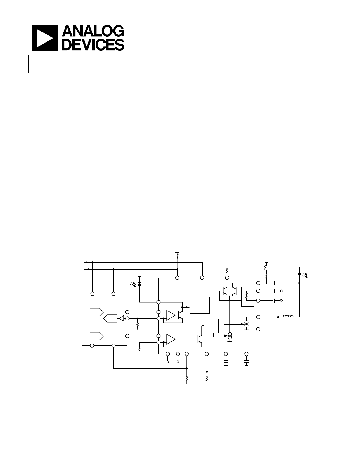
The ADN2871 laser diode driver is designed for advanced SFP
and SFF modules, using SFF-8472 digital diagnostics. The
ADN2871 supports single-rate or multi-rate operation from 50
Mbps to 4.25 Gbps.
Average power and extinction ratio can be set with a voltage
provided by a microcontroller DAC or by a trimmable resistor
or digipot. Average power control-loop is implemented using
feedback from a monitor photodiode. The part provides bias
and modulation current monitoring as well as fail alarms and
automatic laser shutdown. The device interfaces easily with the
ADI ADuC70xx family of microconverters and with the
ADN289x family of limiting amplifiers to make a complete
SFP/SFF transceiver solution. An SFP reference design is
available. The product is pin compatible with the ADN2870
Dual Loop LDD allowing one PC board layout to work with
either device. For dual loop applications, refer to the ADN2870
datasheet.
The product is available in a space-saving 4 mm ×4 mm LFCSP
package specified over the −40°C to +85°C temperature range.
CC
Tx_DISABLE
Tx_FAULT
ADI
MICROCONTROLLER
DAC
ADC
DAC
1kΩ
1kΩ
VCC
GND
GND
MPD
PAVSET
PAVREF
RPAV
ERREF
ERSET
VCC
Figure 1. Application Diagram Showing Microcontroller Interface
Protected by US patent: US6414974
Rev. PrA
Information furnished by Analog Devices is believed to be accurate and reliable.
However, no responsibility is assumed by Analog Devices for its use, nor for any
infringements of patents or other rights of third parties that may result from its use.
Specifications subject to change without notice. No license is granted by implication
or otherwise under any patent or patent rights of Analog Devices. Trademarks and
registered trademarks are the property of their respective owners.
GND
GND GND
VCC
IMODP
IBIAS
NC
L
R
VCC
LASER
DATAP
DATAN
CONTROL
ALSFAIL
X 100
VCC
IMODN
100Ω
IMOD
ADN2871
IBMON IMMON
470Ω1kΩ
One Technology Way, P.O. Box 9106, Norwood, MA 02062-9106, U.S.A.
Tel: 781.329.4700 www.analog.com
Fax: 781.326.8703 © 2004 Analog Devices, Inc. All rights reserved.
GND
PAVCAP
ERCAP
GND
04510-001

ADN2871 Preliminary Technical Data
TABLE OF CONTENTS
Specifications.......................................................................................
SFP Timing Specifications.................................................................
Absolute Maximum Ratings..............................................................
ESD Caution....................................................................................
Pin Configuration and Function Descriptions...............................
Typical Operating Characteristics....................................................
Optical Waveforms Showing Multirate Performance Using
Low Cost Fabry Perot Tosa NEC NX7315UA ............................
Optical Waveforms Showing Dual-Loop Performance Over
Temperature Using DFB Tosa SUMITOMO SLT2486..............
Performance Characteristics.........................................................
Theory of Operation ..........................................................................
Control.............................................................................................
...........................................................................................................
REVISION HISTORY
Voltage Setpoint Calibration..........................................................
Resistor Setpoint Calibration.........................................................
IMPD Monitoring...........................................................................
Loop Bandwidth Selection .............................................................
Power Consumption .......................................................................
Automatic Laser Shutdown (TX_Disable)...................................
Bias and Modulation Monitor Currents.......................................
Data Inputs.......................................................................................
Laser Diode Interfacing..................................................................
Alarms...............................................................................................
Outline Dimensions............................................................................
Ordering Guide ...............................................................................
Revision 0: Initial Version
Rev. PrA | Page 2 of 19

Preliminary Technical Data ADN2871
SPECIFICATIONS
VCC = 3.0 V to 3.6 V. All specifications T
Table 1.
Parameter Min Typ Max Unit Conditions/Comments
LASER BIAS CURRENT (IBIAS)
Output Current IBIAS 2 100 mA
Compliance Voltage 1.2 VCC V
IBIAS when ALS is High 0.2 mA
CCBIAS Compliance Voltage 1.2 V
MODULATION CURRENT (IMODP, IMODN)
Output Current IMOD 5 90 mA
Compliance Voltage 1.5 VCC V
IMOD when ALS is High 0.05 mA
Rise Time
Fall Time
Random Jitter
Deterministic Jitter
Pulse-Width Distortion
2, 3
2, 3
2, 3
2, 3
2, 3
AVERAGE POWER SET (PAVSET)
Pin Capacitance 80 pF
Voltage 1.1 1.2 1.35 V
Photodiode Monitor Current (Average Current) 50 1200 µA Resistor setpoint mode
EXTINCTION RATIO SET INPUT (ERSET)
Resistance Range 1.49 25 kΩ Resistor setpoint mode
Resistance Range 0.99 1.0 1.01 kΩ Voltage setpoint mode
AVERAGE POWER REFERENCE VOLTAGE INPUT (PAVREF)
Voltage Range 0.12 1 V
Photodiode Monitor Current (Average Current) 120 1000 µA
EXTINCTION RATIO REFERENCE VOLTAGE INPUT (ERREF)
Voltage Range 0.05 0.9 V
DATA INPUTS (DATAP, DATAN)
4
V p-p (Differential) 0.4 2.4 V AC-coupled
Input Impedance (Single-Ended) 50 Ω
LOGIC INPUTS (ALS)
VIH 2 V
VIL 0.8 V
ALARM OUTPUT (FAIL)
V
> 1.8 V
OFF
V
ON
5
MIN
2
to T
,1 unless otherwise noted. Typical values as specified at 25°C.
MAX
60 104 ps
60 96 ps
0.8 1.1 ps rms
35 ps 20 mA < IMOD < 90 mA
30 ps 20 mA < IMOD < 90 mA
Voltage setpoint mode
(RPAV fixed at 1 kΩ)
Voltage setpoint mode
(RPAV fixed at 1 kΩ)
Voltage setpoint mode
(RERSET fixed at 1 kΩ)
Voltage required at FAIL for Ibias and
Imod to turn off when FAIL asserted
< 1.3 V
Voltage required at FAIL for Ibias and
Imod to stay on when FAIL asserted
Rev. PrA | Page 3 of 19

ADN2871 Preliminary Technical Data
Parameter Min Typ Max Unit Conditions/Comments
IBMON, IMMON DIVISION RATIO
IBIAS/IBMON
IBIAS/IBMON
IBIAS/IBMON STABILITY
IMOD/IMMON 50 A/A
IBMON Compliance Voltage 0 1.3 V
SUPPLY
7
I
CC
VCC (w.r.t. GND)
1
Temperature range: –40°C to +85°C.
2
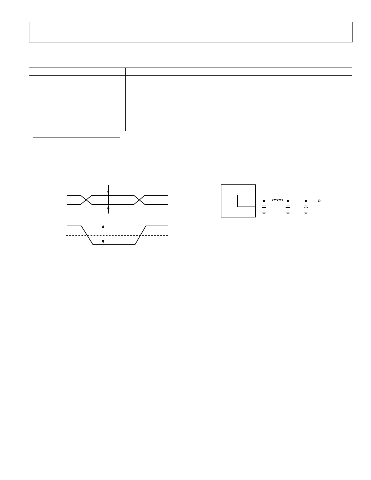
Measured into a 15 Ω load (22 Ω resistor in parallel with digital scope 50 Ω input) using a 11110000 pattern at 2.5 Gbps, shown in Figure 2.
3
Guaranteed by design and characterization. Not production tested.
4
When the voltage on DATAP is greater than the voltage on DATAN, the modulation current flows in the IMODP pin.
5
Guaranteed by design. Not production tested.
6
IBIAS/IBMON ratio stability is defined in SFF-8472 revision 9 over temperature and supply variation.
7
ICC min for power calculation in the Power Consumption section.
8
All VCC pins should be shorted together.
3
3
3, 6
85 100 115 A/A 11 mA < IBIAS < 50 mA
92 100 108 A/A 50 mA < IBIAS < 100 mA
±5 % 10 mA < IBIAS < 100 mA
30 mA When IBIAS = IMOD = 0
8
3.0 3.3 3.6 V
V
CCVCC
ADN2871
IMODP
22Ω
R
L
C
BIAS TEE
80kHz 27GHz
Figure 2. High Speed Electrical Test Output Circuit
TO HIGH SPEED
DIGITAL
OSCILLOSCOPE
50Ω INPUT
04510-034
Rev. PrA | Page 4 of 19

Preliminary Technical Data ADN2871
SFP TIMING SPECIFICATIONS
Table 2.
Parameter Symbol Min Typ Max Unit Conditions/Comments
ALS Assert Time t_off 1 5 µs
ALS Negate Time
Time to Initialize, Including
Reset of FAIL
1
1
t_on 0.83 0.95 ms
t_init 25 275 ms From power-on or negation of FAIL using ALS.
FAIL Assert Time t_fault 100 µs Time to fault to FAIL on.
ALS to Reset time t_reset 5 µs Time TX_DISABLE must be held high to reset TX_FAULT.
1
Guaranteed by design and characterization. Not production tested.
V
SE
DATAP
DATAN
Time for the rising edge of ALS (TX_DISABLE) to when the bias
current falls below 10% of nominal.
Time for the falling edge of ALS to when the modulation current
rises above 90% of nominal.
SFP MODULE
VCC_Tx
1µH
3.3V
0.1µF 0.1µF 10µF
DATAP–DATAN
0V
Figure 3. Signal Level Definition
V p-p
DIFF
= 2× V
SFP HOST BOARD
SE
04510-002
Figure 4. Recommended SFP Supply
04510-003
Rev. PrA | Page 5 of 19

ADN2871 Preliminary Technical Data
ABSOLUTE MAXIMUM RATINGS
TA = 25°C, unless otherwise noted.
Table 3.
Parameter Rating
VCC to GND 4. 2 V
IMODN, IMODP –0.3 V to +4.8 V
PAVCAP –0.3 V to +3.9 V
ERCAP –0.3 V to +3.9 V
PAVSET –0.3 V to +3.9 V
PAVREF –0.3 V to +3.9 V
ERREF –0.3 V to +3.9 V
IBIAS –0.3 V to +3.9 V
IBMON –0.3 V to +3.9 V
IMMON –0.3 V to +3.9 V
ALS –0.3 V to +3.9 V
CCBIAS –0.3 V to +3.9 V
RPAV –0.3 V to +3.9 V
ERSET –0.3 V to +3.9 V
FAIL –0.3 V to +3.9 V
DATAP, DATAN
(single-ended differential)
Junction Temperature 150°C
1.5 V
Stresses above those listed under Absolute Maximum Ratings
may cause permanent damage to the device. This is a stress
rating only; functional operation of the device at these or any
other conditions above those listed in the operational sections
of this specification is not implied. Exposure to absolute
maximum rating conditions for extended periods may affect
device reliability.
Rev. PrA | Page 6 of 19
 Loading...