

3.3 V Dual-Loop, 50 Mbps to 3.3 Gbps
T
FEATURES
SFP/SFF and SFF-8472 MSA-compliant
SFP reference design available
50 Mbps to 3.3 Gbps operation
Multirate 155 Mbps to 3.3 Gbps operation
Dual-loop control of average power and extinction ratio
Typical rise/fall time 60 ps
Bias current range 2 mA to 100 mA
Modulation current range 5 mA to 90 mA
Laser fail alarm and automatic laser shutdown (ALS)
Bias and modulation current monitoring
3.3 V operation
4 mm × 4 mm LFCSP package
Voltage setpoint control
Resistor setpoint control
APPLICATIONS
Multirate OC3 to OC48-FEC SFP/SFF modules
1×/2×/4× Fibre channel SFP/SFF modules
LX-4 modules
DWDM/CWDM SFP modules
1GE SFP/SFF transceiver modules
Laser Diode Driver
ADN2870
GENERAL DESCRIPTION
The ADN2870 laser diode driver is designed for advanced SFP
and SFF modules, using SFF-8472 digital diagnostics. The device
features dual-loop control of the average power and extinction
ratio, which automatically compensates for variations in laser
characteristics over temperature and aging. The laser need only
be calibrated at 25°C, eliminating the need for expensive and
time consuming temperature calibration. The ADN2870 supports
single-rate operation from 50 Mbps to 3.3 Gbps or multirate
from 155 Mbps to 3.3 Gbps.
Average power and extinction ratio can be set with a voltage
provided by a microcontroller DAC or by a trimmable resistor.
The part provides bias and modulation current monitoring as
well as fail alarms and automatic laser shutdown. The device
interfaces easily with the ADI ADuC70xx family of microconverters and with the ADN289x family of limiting amplifiers
to make a complete SFP/SFF transceiver solution. An SFP
reference design is available. The product is available in a spacesaving 4 mm ×4 mm LFCSP package specified over the −40°C to
+85°C temperature range.
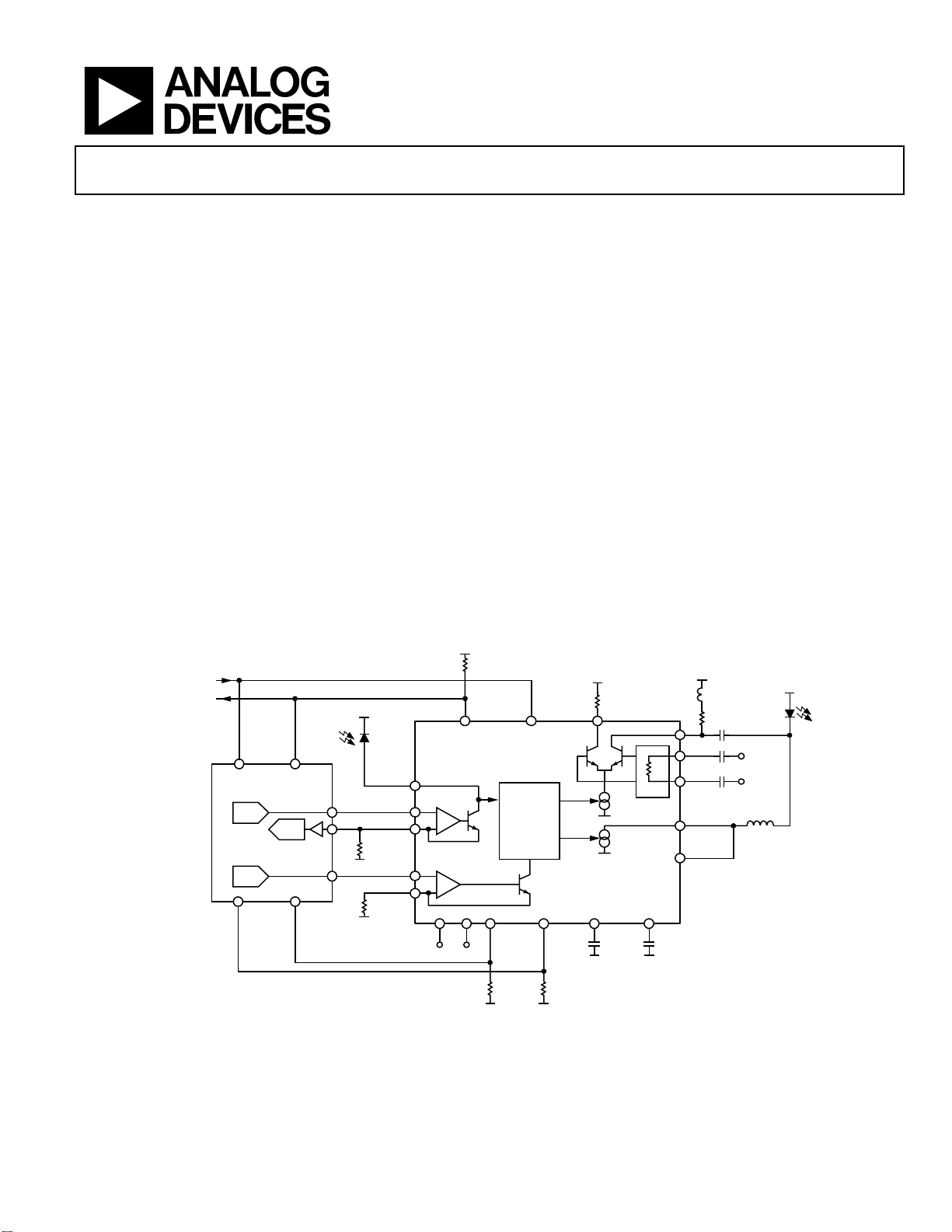
VCC
Tx_FAUL
Tx_FAIL
ADI
MICROCONTROLLER
DAC
ADC
DAC
1kΩ
1kΩ
VCC
GND
GND
MPD
PAVSET
PAVREF
RPAV
ERREF
ERSET
VCC
Figure 1. Application Diagram Showing Microcontroller Interface
Protected by US patent: US6414974
Rev. 0
Information furnished by Analog Devices is believed to be accurate and reliable.
However, no responsibility is assumed by Analog Devices for its use, nor for any
infringements of patents or other rights of third parties that may result from its use.
Specifications subject to change without notice. No license is granted by implication
or otherwise under any patent or patent rights of Analog Devices. Trademarks and
registered trademarks are the property of their respective owners.
GND
GND GND
VCC
L
R
IMODP
IBIAS
CCBIAS
VCC
LASER
DATAP
DATAN
ALSFAIL
CONTROL
IMOD
IBIAS
VCC
IMODN
100Ω
ADN2870
IBMON IMMON
470Ω1kΩ
One Technology Way, P.O. Box 9106, Norwood, MA 02062-9106, U.S.A.
Tel: 781.329.4700
Fax: 781.326.8703 © 2004 Analog Devices, Inc. All rights reserved.
PAVCAP
GND
ERCAP
GND
04510-001
www.analog.com

ADN2870
TABLE OF CONTENTS
Specifications..................................................................................... 3
SFP Timing Specifications............................................................... 5
Absolute Maximum Ratings............................................................ 6
ESD Caution.................................................................................. 6
Pin Configuration and Function Descriptions............................. 7
Typical Operating Characteristics.................................................. 8
Optical Waveforms Showing Multirate Performance Using
Low Cost Fabry Perot Tosa NEC NX7315UA
Optical Waveforms Showing Dual-Loop Performance Over
Temperature Using DFB Tosa SUMITOMO SLT2486
Performance Characteristics....................................................... 9
Theory of Operation ...................................................................... 11
Dual-Loop Control .................................................................... 11
Control......................................................................................... 12
.......................... 8
............ 8
REVISION HISTORY
Volt a ge S etp oint C al i brat ion ..................................................... 12
Resistor Setpoint Calibration.................................................... 14
IMPD Monitoring...................................................................... 14
Loop Bandwidth Selection ........................................................ 15
Power Consumption .................................................................. 15
Automatic Laser Shutdown (T X_Disable).............................. 15
Bias and Modulation Monitor Currents.................................. 15
Data Inputs .................................................................................. 15
Laser Diode Interfacing............................................................. 16
Alarms.......................................................................................... 17
Outline Dimensions....................................................................... 18
Ordering Guide .......................................................................... 18
8/04—Revision 0: Initial Version
Rev. 0 | Page 2 of 20

ADN2870
SPECIFICATIONS
VCC = 3.0 V to 3.6 V. All specifications T
Table 1.
Parameter Min Typ Max Unit Conditions/Comments
LASER BIAS CURRENT (IBIAS)
Output Current IBIAS 2 100 mA
Compliance Voltage 1.2 V
IBIAS when ALS is High 0.2 mA
CCBIAS Compliance Voltage 1.2 V
MODULATION CURRENT (IMODP, IMODN)
Output Current IMOD 5 90 mA
Compliance Voltage 1.5 V
IMOD when ALS is High 0.05 mA
Rise Time
Fall Time
Random Jitter
Deterministic Jitter
Pulse-Width Distortion
2, 3
2, 3
2, 3
2, 3
2, 3
AVERAGE POWER SET (PAVSET)
Pin Capacitance 80 pF
Voltage 1.1 1.2 1.35 V
Photodiode Monitor Current (Average Current) 50 1200 µA Resistor setpoint mode
EXTINCTION RATIO SET INPUT (ERSET)
Resistance Range 1.2 25 kΩ Resistor setpoint mode
Voltage 1.1 1.2 1.35 V Resistor setpoint mode
AVERAGE POWER REFERENCE VOLTAGE INPUT (PAVREF)
Voltage Range 0.12 1 V
Photodiode Monitor Current (Average Current) 120 1000 µA
EXTINCTION RATIO REFERENCE VOLTAGE INPUT (ERREF)
Voltage Range 0.1 1 V
DATA INPUTS (DATAP, DATAN)
4
V p-p (Differential) 0.4 2.4 V AC-coupled
Input Impedance (Single-Ended) 50 Ω
LOGIC INPUTS (ALS)
V
IH
V
IL
ALARM OUTPUT (FAIL)
V
OFF
V
ON
5
MIN
2
to T
,1 unless otherwise noted. Typical values as specified at 25°C.
MAX
CC
V
CC
V
60 104 ps
60 96 ps
0.8 1.1 ps rms
35 ps 20 mA < IMOD < 90 mA
30 ps 20 mA < IMOD < 90 mA
2 V
0.8 V
> 1.8 V
< 1.3 V
Voltage setpoint mode
(RPAV fixed at 1 kΩ)
Voltage setpoint mode
(RPAV fixed at 1 kΩ)
Voltage setpoint mode
(RERSET fixed at 1 kΩ)
Voltage required at FAIL for Ibias and
Imod to turn off when FAIL asserted
Voltage required at FAIL for Ibias and
Imod to stay on when FAIL asserted
Rev. 0 | Page 3 of 20
ADN2870
Parameter Min Typ Max Unit Conditions/Comments
IBMON, IMMON DIVISION RATIO
IBIAS/IBMON
IBIAS/IBMON
IBIAS/IBMON STABILITY
IMOD/IMMON 50 A/A
IBMON Compliance Voltage 0 1.3 V
SUPPLY
7
I
CC
VCC (w.r.t. GND)
1
Temperature range: –40°C to +85°C.
2
Measured into a 15 Ω load (22 Ω resistor in parallel with digital scope 50 Ω input) using a 11110000 pattern at 2.5 Gbps, shown in Figure 2.
3
Guaranteed by design and characterization. Not production tested.
4
When the voltage on DATAP is greater than the voltage on DATAN, the modulation current flows in the IMODP pin.
5
Guaranteed by design. Not production tested.
6
IBIAS/IBMON ratio stability is defined in SFF-8472 revision 9 over temperature and supply variation.
7
ICC min for power calculation in the Power Consumption section.
8
All VCC pins should be shorted together.
3
3
3, 6
85 100 115 A/A 11 mA < IBIAS < 50 mA
92 100 108 A/A 50 mA < IBIAS < 100 mA
±5 % 10 mA < IBIAS < 100 mA
30 mA When IBIAS = IMOD = 0
8
3.0 3.3 3.6 V
V
CCVCC
ADN2870
IMODP
22Ω
R
L
C
BIAS TEE
80kHz → 27GHz
Figure 2. High Speed Electrical Test Output Circuit
TO HIGH SPEED
DIGITAL
OSCILLOSCOPE
50Ω INPUT
04510-034
Rev. 0 | Page 4 of 20
ADN2870
SFP TIMING SPECIFICATIONS
Table 2.
Parameter Symbol Min Typ Max Unit Conditions/Comments
ALS Assert Time t_off 1 5 µs
ALS Negate Time
Time to Initialize, Including
Reset of FAIL
1
1
t_on 0.83 0.95 ms
t_init 25 275 ms From power-on or negation of FAIL using ALS.
FAIL Assert Time t_fault 100 µs Time to fault to FAIL on.
ALS to Reset time t_reset 5 µs Time TX_DISABLE must be held high to reset TX_FAULT.
1
Guaranteed by design and characterization. Not production tested.
V
SE
DATAP
DATAN
Time for the rising edge of ALS (TX_DISABLE) to when the bias
current falls below 10% of nominal.
Time for the falling edge of ALS to when the modulation current
rises above 90% of nominal.
SFP MODULE
VCC_Tx
1µH
3.3V
0.1µF 0.1µF 10µF
DATAP–DATAN
0V
Figure 3. Signal Level Definition
V p-p
DIFF
= 2× V
SFP HOST BOARD
SE
04510-002
Figure 4. Recommended SFP Supply
04510-003
Rev. 0 | Page 5 of 20

ADN2870
ABSOLUTE MAXIMUM RATINGS
TA = 25°C, unless otherwise noted.
Table 3.
Parameter Rating
VCC to GND 4. 2 V
IMODN, IMODP –0.3 V to +4.8 V
PAVCAP –0.3 V to +3.9 V
ERCAP –0.3 V to +3.9 V
PAVSET –0.3 V to +3.9 V
PAVREF –0.3 V to +3.9 V
ERREF –0.3 V to +3.9 V
IBIAS –0.3 V to +3.9 V
IBMON –0.3 V to +3.9 V
IMMON –0.3 V to +3.9 V
ALS –0.3 V to +3.9 V
CCBIAS –0.3 V to +3.9 V
RPAV –0.3 V to +3.9 V
ERSET –0.3 V to +3.9 V
FAIL –0.3 V to +3.9 V
DATAP, DATAN
(single-ended differential)
TEMPERATURE SPECIFICATIONS
Operating Temperature Range
Industrial
Storage Temperature Range –65°C to +150°C
Junction Temperature (TJ max) 150°C
LFCSP Package
Power Dissipation
θJA Thermal Impedance
θJCThermal Impedance 29.5°C/W
Lead Temperature (Soldering 10 s) 300°C
___________________
1
Power consumption equations are provided in the Power Consumption
section.
2
θJA is defined when part is soldered on a 4-layer board.
1
2
1.5 V
−40°C to +85°C
(TJ max – TA)/θJA W
30°C/W
Stresses above those listed under Absolute Maximum Ratings
may cause permanent damage to the device. This is a stress
rating only; functional operation of the device at these or any
other conditions above those listed in the operational sections
of this specification is not implied. Exposure to absolute
maximum rating conditions for extended periods may affect
device reliability.
ESD CAUTION
ESD (electrostatic discharge) sensitive device. Electrostatic charges as high as 4000 V readily accumulate on
the human body and test equipment and can discharge without detection. Although this product features
proprietary ESD protection circuitry, permanent damage may occur on devices subjected to high energy
electrostatic discharges. Therefore, proper ESD precautions are recommended to avoid performance
degradation or loss of functionality.
Rev. 0 | Page 6 of 20

ADN2870
PIN CONFIGURATION AND FUNCTION DESCRIPTIONS
GND
VCC
IMODP
IMODN
GND
IBIAS
18
FAIL
IBMON
ERREF
19
VCC
ADN2870
24
1
CCBIAS
PAVSET
GND
VCC
IMMON
PAVREF
ERSET
RPAV
13
6
12
ALS
DATAN
DATAP
GND
PAVCAP
ERCAP
7
04510-004
Figure 5. Pin Configuration
Table 4. Pin Fuction Descriptions
Pin No. Mnemonic Description
1 CCBIAS Control Output Current
2 PAVSET Average Optical Power Set Pin
3 GND Supply Ground
4 VCC Supply Voltage
5 PAVREF Reference Voltage Input for Average Optical Power Control
6 RPAV Average Power Resistor when Using PAVREF
7 ERCAP Extinction Ratio Loop Capacitor
8 PAVCAP Average Power Loop Capacitor
9 GND Supply Ground
10 DATAP Data, Positive Differential Input
11 DATAN Data, Negative Differential Input
12 ALS Automatic Laser Shutdown
13 ERSET Extinction Ratio Set Pin
14 IMMON Modulation Current Monitor Current Source
15 ERREF Reference Voltage Input for Extinction Ratio Control
16 VCC Supply Voltage
17 IBMON Bias Current Monitor Current Source
18 FAIL FAIL Alarm Output
19 GND Supply Ground
20 VCC Supply Voltage
21 IMODP Modulation Current Positive Output, Connect to Laser Diode
22 IMODN Modulation Current Negative Output
23 GND Supply Ground
24 IBIAS Laser Diode Bias (Current Sink to Ground)
Note: The LFCSP package has an exposed paddle that must be connected to ground.
Rev. 0 | Page 7 of 20

ADN2870
TYPICAL OPERATING CHARACTERISTICS
VCC = 3.3 V and TA = 25°C, unless otherwise noted.
OPTICAL WAVEFORMS SHOWING MULTIRATE
PERFORMANCE USING LOW COST FABRY PEROT TOSA
NEC NX7315UA
Note: No change to PAVCAP and ERCAP values
(ACQ LIMIT TEST) WAVEFORMS 1000
04510-016
31-1
Figure 6. Optical Eye 2.488 Gbps,65 ps/div, PRBS 2
PAV = −4.5 dBm, ER = 9 dB, Mask Margin 25%
(ACQ LIMIT TEST) WAVEFORMS 1000
OPTICAL WAVEFORMS SHOWING DUAL-LOOP
PERFORMANCE OVER TEMPERATURE USING DFB TOSA
SUMITOMO SLT2486
(ACQ LIMIT TEST) WAVEFORMS 1001
04510-047
31-1
Figure 9. Optical Eye 2.488 Gbps, 65 ps/div, PRBS 2
PAV = 0 dBm, ER = 9 dB, Mask Margin 22%, T
(ACQ LIMIT TEST) WAVEFORMS 1001
= 25°C
A
Figure 7. Optical Eye 622 Mbps, 264 ps/div, PRBS 2
PAV = −4.5 dBm, ER = 9 dB, Mask Margin 50%
(ACQ LIMIT TEST) WAVEFORMS 1000
Figure 8. Optical Eye 155 Mbps,1.078 ns/div, PRBS 2
PAV = −4.5 dBm, ER = 9 dB, Mask Margin 50%
31-1
31-1
04510-017
04510-020
Rev. 0 | Page 8 of 20
Figure 10. Optical Eye 2.488 Gbps, 65 ps/div, PRBS 2
PAV = −0.2 dBm, ER = 8.96 dB, Mask Margin 21%, T
31-1
= 85°C
A
04510-048

ADN2870
PERFORMANCE CHARACTERISTICS
90
1.2
1.0
60
RISE TIME (ps)
30
0
0408020 60 100
MODULATION CURRENT (mA)
Figure 11. Rise Time vs. Modulation Current, Ibias = 20 mA
80
60
40
FALL TIME (ps)
20
04510-022
0.8
0.6
JITTER (rms)
0.4
0.2
0
0 204060801
MODULATION CURRENT (mA)
Figure 14. Random Jitter vs. Modulation Current, Ibias = 20 mA
250
220
= 80mA
I
190
160
130
100
TOTAL SUPPLY CURRENT (mA)
70
BIAS
I
BIAS
= 40mA
I
BIAS
= 20mA
04510-037
00
0
0408020 60 100
MODULATION CURRENT (mA)
Figure 12. Fall Time vs. Modulation Current, Ibias = 20 mA
45
40
35
30
25
20
15
10
DETERMINISTIC JITTER (ps)
5
0
20 40 8060 100
MODULATION CURRENT (mA)
Figure 13. Deterministic Jitter vs. Modulation Current, Ibias = 20 mA
04510-025
04510-042
40
0 204060801
MODULATION CURRENT (mA)
Figure 15. Total Supply Current vs. Modulation Current
Total Supply Current = I
+ Ibias + Imod
CC
60
55
50
45
40
35
SUPPLY CURRENT (mA)
30
25
20
–50 –30 –10 10 30 50 70 90 110
Figure 16. Supply Current (I
TEMPERATURE (°C)
) vs. Temperature with ALS Asserted,
CC
Ibias = 20 mA
04510-038
00
04510-027
Rev. 0 | Page 9 of 20

ADN2870
120
115
110
105
100
95
IBIAS/IBMON RATIO
90
85
80
–50 –30 –10 10 30 50 70 90 110
Figure 17. IBIAS/IBMON Gain vs. Temperature, Ibias = 20 mA
TEMPERATURE (°C)
OC48 PRBS31
DATA TRANSMISSION
t
LESS THAN 1µs
_OFF
04510-028
60
58
56
54
52
50
48
IMOD/IMMON RATIO
46
44
42
40
–50 –30 –10 10 30 50 70 90 110
TEMPERATURE (°C)
Figure 20. IMOD/IMMON Gain vs. Temperature, Imod = 30 mA
FAIL ASSERTED
04510-031
ALS
Figure 18. ALS Assert Time, 5 µs/div
OC48 PRBS31
DATA TRANSMISSION
t
_ON
ALS
Figure 19. ALS Negate Time, 200 µs/div
04510-029
04510-032
FAULT FORCED ON PAVSET
04510-045
Figure 21. FAIL Assert Time,1 µs/div
TRANSMISSION ON
POWER SUPPLY TURN ON
04510-046
Figure 22. Time to Initialize, Including Reset, 40 ms/div
Rev. 0 | Page 10 of 20

ADN2870
THEORY OF OPERATION
Gm
OPTICAL COUPLING
BIAS
SHA
Φ
1
CURRENT
MOD
SHA
Φ
2
BIAS
SWITCH
CURRENT
HIGH
SPEED
MOD
VCC
Φ
100 2
Laser diodes have a current-in to light-out transfer function as
shown in Figure 23. Two key characteristics of this transfer
function are the threshold current, Ith, and slope in the linear
region beyond the threshold current, referred to as slope
efficiency, LI.
P1
ER =
P
O
P1 + P
P1
P
AV
P
AV
OPTICAL POWER
P
O
O
=
2
∆
P
∆
I
Ith CURRENT
LI =
∆
P
∆
I
04510-005
Figure 23. Laser Transfer Function
DUAL-LOOP CONTROL
Typically laser threshold current and slope efficiency are both
functions of temperature. For FP and DFB type lasers the
threshold current increases and the slope efficiency decreases
with increasing temperature. In addition, these parameters vary
as the laser ages. To maintain a constant optical average power
and a constant optical extinction ratio over temperature and
laser lifetime, it is necessary to vary the applied electrical bias
current and modulation current to compensate for the lasers
changing LI characteristics.
Single-loop compensation schemes use the average monitor
photodiode current to measure and maintain the average
optical output power over temperature and laser aging. The
ADN2870 is a dual-loop device, implementing both this
primary average power control loop and, additionally, a
secondary control loop, which maintains constant optical
extinction ratio. The dual-loop control of average power and
extinction ratio implemented in the ADN2870 can be used
successfully both with lasers that maintain good linearity of LI
transfer characteristics over temperature and with those that
exhibit increasing nonlinearity of the LI characteristics over
temperature.
Dual Loop
The ADN2870 uses a proprietary patented method to control
both average power and extinction ratio. The ADN2870 is
constantly sending a test signal on the modulation current
signal and reading the resulting change in the MPD current as a
means of detecting the slope of the laser in real time. This
information is used in a servo to control the ER of the laser,
which is done in a time-multiplexed manner at a low frequency,
typically 80 Hz. Figure 24 shows the dual-loop control
implementation on the ADN2870.
MPD
INPUT
Φ
2
1.2V
V
BGAP
I
PA
I
ERSET
EX
PAVSET
Figure 24. Dual-Loop Control of Average Power and Extinction Ratio
A dual loop is made up of an APCL (average power control
loop) and the ERCL (extinction ratio control loop), which are
separated into two time states. During time Φ1, the APC loop is
operating, and during time Φ2, the ER loop is operating.
Average Power Control Loop
The APCL compensates for changes in Ith and LI by varying
Ibias. APC control is performed by measuring MPD current,
Impd. This current is bandwidth-limited by the MPD. This is
not a problem because the APCL must be low frequency since
the APCL must respond to the average current from the MPD.
The APCL compares Impd × Rpavset to the BGAP voltage,
Vbgap. If Impd falls, the bias current is increased until Impd ×
Rpavset equals Vbgap. Conversely, if the Impd increases, Ibias
is decreased.
Modulation Control Loop
The ERCL measures the slope efficiency, LI, of the LD, and
changes Imod as LI changes. During the ERCL, Imod is
temporarily increased by ∆Imod. The ratio between Imod and
∆Imod is a fixed ratio of 50:1, but during startup, this ratio is
increased in order to decrease settling time.
During ERCL, switching in ∆Imod causes a temporary increase
in average optical power, ∆Pav. However the APC loop is disabled during ERCL, and the increase is kept small enough so as
not to disturb the optical eye. When ∆Imod is switched into the
laser circuit, an equal current, Iex, is switched into the PAVSET
resistor. The user sets the value of Iex; this is the ERSET setpoint.
If ∆Impd is too small, the control loop knows that LI has
decreased and increases Imod and, therefore, ∆Imod accordingly
until ∆Impd is equal to Iex. The previous time state values of
the bias and mod settings are stored on the hold capacitors
PAVCAP a n d ERCAP.
The ERCL is constantly measuring the actual LI curve, therefore
it compensates for the effects of temperature and for changes in
the LI curve due to laser aging. Thus the laser may be calibrated
once at 25°C and can then automatically control the laser over
temperature. This eliminates expensive and time consuming
temperature calibration of the laser.
2
04510-039
Rev. 0 | Page 11 of 20

ADN2870
××=
Operation with Lasers with Temperature-Dependent
Nonlinearity of Laser LI Curve
The ADN2870 ERCL extracts information from the monitor
photodiode signal relating to the slope of the LI characteristics
at the optical 1 level (P1). For lasers with good linearity over
temperature, the slope measured by the ADN2870 at the optical
1 level is representative of the slope anywhere on the LI curve.
This slope information is used to set the required modulation
current to achieve the required optical extinction ratio.
4.0
RELATIVELY LINEAR LI CURVE AT 25°C
3.5
3.0
2.5
2.0
1.5
OPTICAL POWER (mW)
1.0
0.5
0
0
20 40 60
Figure 25. Measurement of a Laser LI Curve Showing
Laser Nonlinearity at High Temperatures
Some types of laser have LI curves that become progressively
more nonlinear with increasing temperature (see Figure 25). At
temperatures where the LI curve shows significant nonlinearity,
the LI curve slope measured by the ADN2870 at the optical 1
level is no longer representative of the overall LI curve. It is
evident that applying a modulation current based on this slope
information cannot maintain a constant extinction ratio over
temperature. However, the ADN2870 can be configured to
maintain near constant optical bias and extinction ratio with a
laser exhibiting a monotonic temperature-dependant nonlinearity. To implement this correction, it is necessary to characterize
a small sample of lasers for their typical nonlinearity by
measuring them at two temperature points, typically 25°C and
85°C. The measured nonlinearity is used to determine the
amount of feedback to apply. Typically one must characterize 5
to 10 lasers of a particular model to get a good number. Then
the product can be calibrated at 25°C only, avoiding the expense
of temperature calibration. Typically the microcontroller
supervisor is used to measure the laser and apply the feedback.
This scheme is particularly suitable for circuits that already use
a microcontroller for control and digital diagnostic monitoring.
NONLINEAR LI CURVE AT 80°C
CURRENT (mA)
04510-008
10080
The ER correction scheme, while using the average nonlinearity
for the laser population, in fact, supplies a corrective measurement based on each laser’s actual performance as measured
during operation. The ER correction scheme corrects for errors
due to laser nonlinearity while the dual loop continues to adjust
for changes in the Laser LI.
For more details on maintaining average optical power and
extinction ratio over temperature when working with lasers
displaying a temperature dependant nonlinearity of LI curve,
see Application Note AN-743.
CONTROL
The ADN2870 has two methods for setting the average power
(PAV) and extinction ratio (ER). The average power and
extinction ratio can be voltage-set using a microcontroller’s
voltage DACs outputs to provide controlled reference voltages
PAVREF and ERREF. Alternatively, the average power and
extinction ratio can be resistor-set using potentiometers at the
PAVSET and ERSET pins, respectively.
VOLTAGE SETPOINT CALIBRATION
The ADN2870 allows interface to a microcontroller for both
control and monitoring (see Figure 26). The average power at
the PAVSET pin and extinction ratio at the ERSET pin can be
set using the microcontroller’s DACs to provide controlled
reference voltages PAVREF and ERREF. Note that during power
up, there is an internal sequence that allows 25 ms before
enabling the alarms; therefore the customer must ensure that
the voltage for PAVREF and ERREF are active within 20 ms.
RPAVRPPAVREF
SPAV
RERREF ×
ERSET
I
where:
R
is the monitor photodiode responsivity.
SP
is the dc optical power specified on the laser data sheet.
P
CW
is MPD current at that specified PCW.
I
MPD_CW
P
is the average power required.
AV
ER is the desired extinction ratio (ER = P1/P0).
In voltage setpoint, RPAV and R
a 1% tolerance and a temperature coefficient of 50 ppm/°C.
(Volts)
ER
−
_
CWMPD
P
CW
ERSET
1
××=
ER
P
(Volts)
AV
+
1
must be 1 kΩ resistors with
Rev. 0 | Page 12 of 20

ADN2870
T
Tx_FAUL
Tx_FAIL
MICROCONTROLLER
ADI
DAC
ADC
DAC
1kΩ
1kΩ
VCC
GND
GND
MPD
PAVSET
PAVREF
RPAV
ERREF
ERSET
VCC
VCC
GND
GND GND
ALSFAIL
IMOD
CONTROL
IBMON IMMON
IBIAS
470Ω1kΩ
VCC
IMODN
ADN2870
PAVCAP
GND
100Ω
GND
ERCAP
VCC
L
R
IMODP
IBIAS
CCBIAS
LASER
DATAP
DATAN
VCC
04510-009
Figure 26. ADN2870 Using Microconverter Calibration and Monitoring
ERCAP
VCC
L
R
IMODP
IBIAS
CCBIAS
LASER
DATAP
DATAN
VCC
04510-010
VCC
GND
GND
MPD
VCC
VCC
PAVREF
RPAV
PAVSET
ERSET
ERREF
VCC
VCC
GND
GND GND
ALSFAIL
IMOD
CONTROL
IBMON IMMON
IBIAS
470Ω1kΩ
VCC
IMODN
ADN2870
PAVCAP
GND
100Ω
GND
Figure 27. ADN2870 Using Resistor Setpoint Calibration of Average Power and Energy Ratio
Rev. 0 | Page 13 of 20

ADN2870
P
AV
V
RESISTOR SETPOINT CALIBRATION
In resistor setpoint calibration. PAVREF, ERREF, and RPAV
must all be tied to VCC. Average power and extinction ratio can
be set using the PAVSET and ERSET pins, respectively. A
resistor is placed between the pin and GND to set the current
flowing in each pin as shown in Figure 27. The ADN2870
ensures that both PAVSET and ERSET are kept 1.2 V above
GND. The PAVSET and ERSET resistors are given by the
following:
V23.1
CW
µ
RP
×
_
CWMPD
C ADC
INPUT
(Ω)
S
V23.1
ER
−
1
ER
CC
+
+
1
R
1kΩ
×
(Ω)
P
AV
PAVSET
ADN2870
RPAV
04510-043
PAVSET
ERSET
=
=
I
R
R
P
where:
R
is the monitor photodiode responsivity.
SP
is the dc optical power specified on the laser data sheet.
P
CW
I
is MPD current at that specified PCW.
MPD_CW
is the average power required.
P
AV
ER is the desired extinction ratio (ER = P1/P0).
IMPD MONITORING
IMPD monitoring can be implemented for voltage setpoint and
resistor setpoint as follows.
Voltage Setpoint
In voltage setpoint calibration, the following methods may be
used for IMPD monitoring.
Method 1: Measuring Voltage at RPAV
The IMPD current is equal to the voltage at RPAV divided by
the value of RPAV (see Figure 28) as long as the laser is on and
is being controlled by the control loop. This method does not
provide a valid IMPD reading when the laser is in shut-down or
fail mode. A microconverter buffered A/D input may be connected to RPAV to make this measurement. No decoupling or
filter capacitors should be placed on the RPAV node because
this can disturb the control loop.
PHOTODIODE
Figure 28. Single Measurement of IMPD RPAV in Voltage Setpoint Mode
Method 2: Measuring IMPD Across a Sense Resistor
The second method has the advantage of providing a valid IMPD
reading at all times, but has the disadvantage of requiring a
differential measurement across a sense resistor directly in
series with the IMPD. As shown in Figure 29, a small resistor,
Rx, is placed in series with the IMPD. If the laser used in the
design has a pinout where the monitor photodiode cathode and
the lasers anode are not connected, a sense resistor can be placed
in series with the photodiode cathode and VCC as shown in
Figure 30. When choosing the value of the resistor, the user
must take into account the expected IMPD value in normal
operation. The resistor must be large enough to make a significant signal for the buffered A/Ds to read, but small enough so as
not to cause a significant voltage reduction across the IMPD.
The voltage across the sense resistor should not exceed 250 mV
when the laser is in normal operation. It is recommended that a
10 pF capacitor be placed in parallel with the sense resistor.
VCC
LDPHOTODIODE
µ
C ADC
DIFFERENTIAL
INPUT
Figure 29. Differential Measurement of IMPD Across a Sense Resistor
µ
C ADC
INPUT
PHOTODIODE
Figure 30. Single Measurement of IMPD Across a Sense Resistor
ADN2870
200Ω
RESISTOR
ADN2870
200Ω
RESISTOR
PAVSET
VCC VCC
PAVSET
10pF
04510-011
LD
04510-011
Resistor Setpoint
In resistor setpoint calibration, the current through the resistor
from PAVSET to ground is the IMPD current. The recommended
method for measuring the IMPD current is to place a small
resistor in series with PAVSET resistor (or potentiometer) and
measure the voltage across this resistor as shown in Figure 31.
The IMPD current is then equal to this voltage divided by the
value of resistor used. In resistor setpoint, PAVSET is held to
1.2 V nominal; it is recommended that the sense resistor should
be selected so that the voltage across the sense resistor does not
exceed 250 mV.
Rev. 0 | Page 14 of 20

ADN2870
V
V
V
d
PHOTODIODE
µ
C ADC
INPUT
Figure 31. Single Measurement of IMPD Across a
Sense Resistor in Resistor Setpoint IMPD Monitoring
CC
R
PAVSET
ADN2870
04510-040
LOOP BANDWIDTH SELECTION
To ensure that the ADN2870 control loops have sufficient
bandwidth, the average power loop capacitor (PAVCAP) and
the extinction ratio loop capacitor (ERCAP) are calculated
using the lasers slope efficiency (watts/amps) and the average
power required.
For resistor point control:
EPAVCAP ×−=
ERCAP =
PAVCAP
LI
PA
For voltage setpoint control:
EPAVCAP ×−=
ERCAP =
PAVCAP
LI
PA
where PAV is the average power required and LI (mW/mA) is
the typical slope efficiency at 25°C of a batch of lasers that are
used in a design. The capacitor value equation is used to get a
centered value for the particular type of laser that is used in a
design and average power setting. The laser LI can vary by a
factor of 7 between different physical lasers of the same type
and across temperature without the need to recalculate the
PAVCAP and ERCAP values. In ac coupling configuration the
LI can be calculated as follows:
P0P1LI−
=
Imo
(mW/mA)
where P1 is the optical power (mW) at the one level, and P0 is
the optical power (mW) at the zero level.
These capacitors are placed between the PAVCAP and ERCAP
pins and ground. It is important that these capacitors are low
leakage multilayer ceramics with an insulation resistance
greater than 100 GΩ or a time constant of 1000 sec, whichever
is less. The capacitor tolerance may be ±30% from the calculated
value to the available off the shelf value including the capacitors
own tolerance.
)(62.3 Farad
)(2Farad
)(628.1 Farad
)(2Farad
POWER CONSUMPTION
The ADN2870 die temperature must be kept below 125°C. The
LFCSP package has an exposed paddle, which should be connected such that is at the same potential as the ADN2870 ground
pins. Power consumption can be calculated as follows:
= ICC min + 0.3 I
I
CC
P = V
× ICC + (I
CC
MODN_PIN
= T
DIE
)/2
AMBIENT
+ θJA × P
V
T
Thus, the maximum combination of I
BIAS
MOD
× V
BIAS_PIN
) + I
BIAS
MOD
+ I
(V
MOD
MODP_PIN
must be
+
calculated.
where:
min = 30 mA, the typical value of ICC provided in the
I
CC
= I
Specifications with I
is the die temperature.
T
DIE
is the ambient temperature.
T
AMBIENT
is the voltage at the IBIAS pin.
V
BIAS_PIN
V
V
is the voltage at the IMODP pin.
MODP_PIN
is the voltage at the IMODN pin.
MODN_PIN
BIAS
MOD
= 0.
AUTOMATIC LASER SHUTDOWN (TX_DISABLE)
ALS (TX disable) is an input that is used to shut down the
transmitter optical output. The ALS pin is pulled up internally
with a 6 kΩ resistor, and conforms to SFP MSA specification.
When ALS is logic high or when open, both the bias and
modulation currents are turned off.
BIAS AND MODULATION MONITOR CURRENTS
IBMON and IMMON are current-controlled current sources
that mirror a ratio of the bias and modulation current. The
monitor bias current, IBMON, and the monitor modulation
current, IMMON, should both be connected to ground through
a resistor to provide a voltage proportional to the bias current
and modulation current, respectively. When using a microcontroller, the voltage developed across these resistors can be
connected to two of the ADC channels, making available a
digital representation of the bias and modulation current.
DATA INPUTS
Data inputs should be ac-coupled (10 nF capacitors are
recommended) and are terminated via a 100 Ω internal resistor
between the DATAP and DATAN pins. A high impedance
circuit sets the common-mode voltage and is designed to allow
maximum input voltage headroom over temperature. It is
necessary to use ac coupling to eliminate the need for matching
between common-mode voltages.
Rev. 0 | Page 15 of 20

ADN2870
LASER DIODE INTERFACING
The schematic in Figure 32 describes the recommended circuit
for interfacing the ADN2870 to most TO-Can or Coax lasers.
These lasers typically have impedances of 5 Ω to 7 Ω, and have
axial leads. The circuit shown works over the full range of data
rates from 155 Mbps to 3.3 Gbps including multirate operation
(with no change to PAVCAP and ERCAP values); see the
Typical Operating Characteristics for multirate performance
examples. Coax lasers have special characteristics that make
them difficult to interface to. They tend to have higher
inductance, and their impedance is not well controlled. The
circuit in Figure 32 operates by deliberately misterminating the
transmission line on the laser side, while providing a very high
quality matching network on the driver side. The impedance of
the driver side matching network is very flat versus frequency
and enables multirate operation. A series damping resistor
should not be used.
VCC
L (0.5nH)
C
R
P
100nF
IMODP
ADN2870
IBIAS
CCBIAS
24Ω
30Ω
Tx LINE
L
30Ω
Tx LINE
BLMI8HG60ISN1D
Figure 32. Recommended Interface for ADN2870 AC Coupling
R 24Ω
C 2.2pF
VCC
04510-014
The 30 Ω transmission line used is a compromise between drive
current required and total power consumed. Other transmission
line values can be used, with some modification of the component values. The R and C snubber values in Figure 32, 24 Ω and
2.2 pF, respectively, represent a starting point and must be tuned
for the particular model of laser being used. R
, the pull-up
P
resistor is in series with a very small (0.5 nH) inductor. In some
cases, an inductor is not required or can be accommodated with
deliberate parasitic inductance, such as a thin trace or a via,
placed on the PC board.
Care should be taken to mount the laser as close as possible to
the PC board, minimizing the exposed lead length between the
laser can and the edge of the board. The axial lead of a coax
laser are very inductive (approximately 1 nH per mm). Long
exposed leads result in slower edge rates and reduced eye margin.
Recommended component layouts and gerber files are available
by contacting the factory. Note that the circuit in Figure 32 can
supply up to 56 mA of modulation current to the laser, sufficient
for most lasers available today. Higher currents can be accommodated by changing transmission lines and backmatch values;
contact factory for recommendations. This interface circuit is
not recommended for butterfly-style lasers or other lasers with
25 Ω characteristic impedance. Instead, a 25 Ω transmission line
and inductive (instead of resistive) pull-up is recommended;
contact the factory for recommendations.
The ADN2870 also supports differential drive schemes. These
can be particularly useful when driving VCSELs or other lasers
with slow fall times. Differential drive can be implemented by
adding a few extra components. A possible implementation is
shown in Figure 33.
V
CC
L1 = 0.5nH
R1 = 15Ω
IMODN
ADN2870
IMODP
CCBIAS IBIAS
SNUBBER SETTINGS: 40Ω AND 1.5pF, NOT OPTIMIZED,
OPTIMIZATION SHOULD CONSIDER PARASITIC.
R1 = 15Ω
(12 TO 24Ω)
V
CC
Figure 33. Recommended Differential Drive Circuit
C1 = C2 = 100nF
20Ω TRANMISSION LINES
L2 = 0.5nH
Rev. 0 | Page 16 of 20
L4 = BLM18HG601SN1
L3 = 4.7nH
C3
R3
SNUBBER
L5 = 4.7nH
L6 = BLM18HG601SN1
TOCAN/VCSEL
LIGHT
04510-041

ADN2870
ALARMS
The ADN2870 has a latched active high monitoring alarm (FAIL).
The FAIL alarm output is an open drain in conformance to SFP
MSA specification requirements.
The ADN2870 has a 3-fold alarm system that covers
• Use of a bias current higher than expected, probably as a
result of laser aging.
• Undervoltage in IBIAS node (laser diode cathode) that
would increase the laser power.
The bias current alarm trip point is set by selecting the value of
resistor on the IBMON pin to GND. The alarm is triggered
when the voltage on the IBMON pin goes above 1.2 V.
FAIL is activated when the single-point faults in Table 5 occur.
• Out-of-bounds average voltage at the monitor photodiode
(MPD) input, indicating an indicating an excessive amount
of laser power or a broken loop.
Table 5. ADN2870 Single-Point Alarms
Alarm Type Pin Name Over Voltage or Short to VCC Condition Under Voltage or Short to GND Condition
1. Bias Current IBMON Alarm if > 1.2 V Ignore
2. MPD Current PAVSET Alarm if > 1.7 V Alarm if < 0.9 V
ERREF Alarm if shorted to VCC Alarm if shorted to GND 3. Crucial Nodes
IBIAS Ignore Alarm if < 600 mV
Table 6. ADN2870 Response to Various Single-Point Faults in AC-Coupled Configuration as Shown in Figure 32
Pin Short to VCC Short to GND Open
CCBIAS Fault state occurs Fault state occurs Does not increase laser average power
PAVSET Fault state occurs Fault state occurs Fault state occurs
PAVREF
RPAV
ERCAP Does not increase laser average power Does not increase laser average power Does not increase laser average power
PAVCAP Fault state occurs Fault state occurs Fault state occurs
DATAP Does not increase laser average power Does not increase laser average power Does not increase laser average power
DATAN Does not increase laser average power Does not increase laser average power Does not increase laser average power
ALS Output currents shut off Normal currents Output currents shut off
ERSET Does not increase laser average power Does not increase laser average power Does not increase laser average power
IMMON Does not affect laser power Does not increase laser average power Does not increase laser average power
ERREF
IBMON Fault state occurs Does not increase laser average power Does not increase laser average power
FAIL Fault state occurs Does not increase laser average power Does not increase laser average power
IMODP Does not increase laser average power Does not increase laser average power Does not increase laser average power
IMODN Does not increase laser average power Does not increase laser average power Does not increase laser power
IBIAS Fault state occurs Fault state occurs Fault state occurs
Voltage mode: Fault state occurs
Resistor mode: Tied to VCC
Voltage mode: Fault state occurs
Resistor mode: Tied to VCC
Voltage mode: Fault state occurs
Resistor mode: Tied to VCC
Fault state occurs Fault state occurs
Fault state occurs
Voltage mode: Does not increase
average power
Resistor mode: Fault state occurs
Voltage mode: Fault state occurs
Resistor mode: Does not increase
average power
Does not increase laser average power
Rev. 0 | Page 17 of 20

ADN2870
OUTLINE DIMENSIONS
0.08
0.60 MAX
19
18
BOTTOM
13
12
VIEW
24
7
1
6
2.50 REF
PIN 1
INDICATOR
2.25
2.10 SQ
1.95
0.25 MIN
4.00
PIN 1
INDICATOR
1.00
0.85
0.80
SEATING
PLANE
12° MAX
BSC SQ
TOP
VIEW
0.80 MAX
0.65TYP
COMPLIANT TO JEDECSTANDARDSMO-220-VGGD-2
0.30
0.23
0.18
3.75
BSC SQ
0.20 REF
0.60 MAX
0.05 MAX
0.02 NOM
0.50
BSC
0.50
0.40
0.30
COPLANARITY
Figure 34. 24-Lead Lead Frame Chip Scale Package [LFCSP]
(CP-24)
Dimensions shown in millimeters
Note: The LFCSP package has an exposed paddle that must be connected to ground.
ORDERING GUIDE
Model Temperature Range Package Description Package Option
ADN2870ACPZ
ADN2870ACPZ-RL
ADN2870ACPZ-RL7
1
1
1
−40°C to +85°C
−40°C to +85°C
−40°C to +85°C
24-Lead Lead Frame Chip Scale Package CP-24
24-Lead Lead Frame Chip Scale Package CP-24
24-Lead Lead Frame Chip Scale Package CP-24
1
Z = Pb-free part.
Rev. 0 | Page 18 of 20

Preliminary Technical Data ADN2870
NOTES
Rev. 0 | Page 19 of 20

ADN2870
NOTES
© 2004 Analog Devices, Inc. All rights reserved. Trademarks and
registered trademarks are the property of their respective owners.
D04510–0–8/04(0)
Rev. 0 | Page 20 of 20
 Loading...