Continuous Rate 12.3Mb/s to 2.7Gb/s
www.BDTIC.com/ADI
Clock and Data Recovery IC w/Loop Timed SERDES
Preliminary Technical Data
FEATURES
Serial data input: 12.3 Mb/s to 2.7 Gb/s
Exceeds ITU-T Jitter Specifications
Integrated Limiting Amp: 6mV sensitivity
Adjustable slice level: ±100 mV
Patented dual-loop clock recovery architecture
Programmable LOS detect and Slice Level
Integrated PRBS Generator and Detector
No reference clock required
Loss of lock indicator
Rate Selectivity without the use of a reference clock
2
C™ interface to access optional features
I
Single-supply operation: 3.3 V
Low power: 1.0W
8 mm × 8 mm 56-lead LFCSP
APPLICATIONS
Passive Optical Network s
SONET OC-1/3/12/48 and all associated FEC rates
Fibre Channel, 2× Fibre Channel , GbE, HDTV, etc.
WDM transponders
Test equipment
ADN2865
PRODUCT DESCRIPTION
The ADN2865 provides the receiver functions of quantization,
signal level detect, and clock and data recovery for continuous
data rates from 12.3 Mb/s to 2.7 Gb/s. An integrated
deserialiser supports 8 bit parallel transfer to an FPGA or digital
ASIC. The recovered clock can simultaneously serialize data
supplied in an 8 bit parallel format.
The ADN2865 automatically locks to all data rates without the
need for an external reference clock or programming. All
SONET jitter requirements are exceeded, including jitter
transfer, jitter generation, and jitter tolerance. All specifications
are quoted for −40°C to +85°C ambient temperature, unless
otherwise noted.
This device, together with a PIN diode and a TIA preamplifier,
can implement a highly integrated, low cost, low power fiber
optic receiver.
The ADN2865 have many optional features available via an I
interface, e.g. the user can read back the data rate that the
ADN2865 is locked on to, or the user can set the device to only
lock to one particular data rate if provisioning of data rates is
required.
2
C
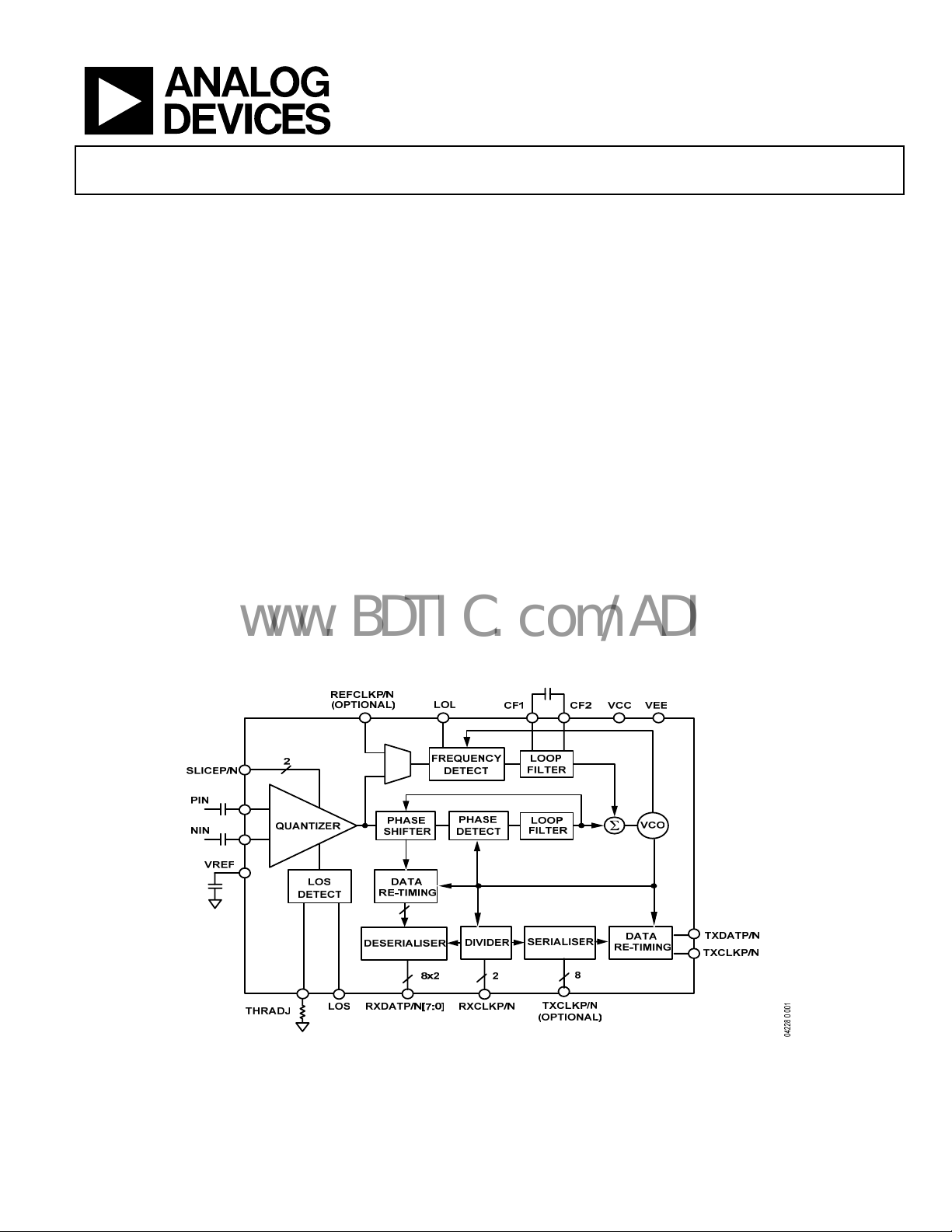
FUNCTIONAL BLOCK DIAGRAM
Figure 1 ADN2865 Functional Block Diagram
Rev.PrA
Information furnished by Analog Devices is believed to be accurate and reliable.
However, no responsibility is assumed by Analog Devices for its use, nor for any
infringements of patents or other rights of third parties that may result from its use.
Specifications subject to change without notice. No license is granted by implication
or otherwise under any patent or patent rights of Analog Devices. Trademarks and
registered trademarks are the property of their respective owners.
One Technology Way, P.O. Box 9106, Norwood, MA 02062-9106, U.S.A.
Tel: 781.329.4700 www.analog.com
Fax: 781.326.8703 © 2006 Analog Devices, Inc. All rights reserved.

ADN2865 Preliminary Technical Data
www.BDTIC.com/ADI
TABLE OF CONTENTS
Specifications..................................................................................... 3
Jitter Specifications....................................................................... 4
Output and Timing Specifications ............................................. 5
Absolute Maximum Ratings............................................................ 6
Thermal Characteristics .............................................................. 7
ESD Caution.................................................................................. 7
Timing Characteristics..................................................................... 9
Pin Configuration and Function Descriptions........................... 10
Typical Performance Characteristics ............................................. 8
2
I
C Interface Timing and Internal Register Description........... 12
Terminology .................................................................................... 16
Jitter Specifications ......................................................................... 17
Jitter Generation .........................................................................17
Jitter Transfer............................................................................... 17
Jitter Tolerance............................................................................ 17
Functional Description.................................................................. 20
Frequency Acquisition............................................................... 20
Limiting Amplifier ..................................................................... 21
Slice Adjust.................................................................................. 22
Loss of Signal (LOS) Detector .................................................. 22
Lock Detector Operation .......................................................... 20
Harmonic Detector.................................................................... 21
Squelch Mode .......................... Error! Bookmark not defined.
I2C Interface ............................................................................... 22
Reference Clock (Optional) ...................................................... 23
Applications Information.............................................................. 26
PCB Design Guidelines ............................................................. 26
DC-Coupled Application.......................................................... 28
Coarse Data Rate Readback Look-Up Table............................... 30
Outline Dimensions....................................................................... 32
Theory of Operation ...................................................................... 18
REVISION HISTORY
Revision 0: Initial Version
Revision A: Remove Minimum Supply Current Spec
Revision B: Update spec table
Ordering Guide .......................................................................... 32
Rev. PrA | Page 2 of 33

Preliminary Technical Data ADN2865
www.BDTIC.com/ADI
SPECIFICATIONS
TA = T
unless otherwise noted.
Table 1.
Parameter Conditions Min Typ Max Unit
QUANTIZER—DC CHARACTERISTICS
QUANTIZER—AC CHARACTERISTICS
QUANTIZER—SLICE ADJUSTMENT
LOSS OF SIGNAL DETECT (LOS)
R
R
R
OC-1
R
R
LOSS OF LOCK DETECT (LOL)
OC-48 1.0 μs
ACQUISITION TIME
OC-12 2.0 ms
OC-3 3.4 ms
OC-1 9.8 ms
12.3 Mb/s 40.0 ms
1
PIN and NIN should be differentially driven and ac-coupled for optimum sensitivity.
2
When ac-coupled, the LOS assert and de-assert time is dominated by the RC time constant of the ac coupling capacitor and the 50 Ω input termination of the
ADN2865 input stage.
MIN
to T
, VCC = V
MAX
MIN
to V
, VEE = 0 V, CF = 0.47 μF, SLICEP = SLICEN = VEE, Input Data Pattern: PRBS 223 − 1,
MAX
Input Voltage Range @ PIN or NIN, dc-coupled 1.8 2.8 V
Peak-to-Peak Differential Input PIN – NIN 2.0 V
Input Common Mode Level
DC-coupled (see Figure , Figure , and
Figure )
Differential Input Sensitivity 223 − 1 PRBS, ac-coupled,1 BER = 1 x 10
2.3 2.5
–10
TBD TBD mV p-p
2.8
V
Input Overdrive (see Figure ) TBD TBD mV p-p
Input Offset TBD μV
Input RMS Noise BER = 1 x 10
–10
TBD μV rms
Data Rate 12.3 2700 Mb/s
S11 @ 2.5 GHz −15 dB
Input Resistance Differential 100
Ω
Input Capacitance 0.65 pF
Gain SLICEP – SLICEN = ±0.5 V TBD 0.1 TBD V/V
Differential Control Voltage Input SLICEP – SLICEN TBD V
Control Voltage Range DC level @ SLICEP or SLICEN VEE 0.95 V
Slice Threshold Offset 1 mV
Loss of Signal Detect Range (see Figure 2) R
= 0 Ω TBD TBD mV
Thresh
= 100 kΩ TBD TBD mV
Thresh
Hysteresis (Electrical) OC-48
= 0 Ω TBD TBD dB
Thresh
= 100 kΩ TBD TBD dB
Thresh
= 0 Ω TBD TBD dB
Thresh
= 10 kΩ TBD TBD dB
Thresh
LOS Assert Time DC-coupled2 TBD ns
LOS De-Assert Time DC-coupled2 TBD ns
VCO Frequency Error for LOL Assert With respect to nominal 1000 ppm
VCO Frequency Error for LOL De-Assert With respect to nominal 250 ppm
LOL Response Time 12.3 Mb/s 4 ms
OC-12 1.0 μs
Lock to Data Mode OC-48 1.3 ms
Optional Lock to REFCLK Mode 10.0 ms
Rev. PrA | Page 3 of 33
ADN2865 Preliminary Technical Data
www.BDTIC.com/ADI
Parameter Conditions Min Typ Max Unit
DATA RATE READBACK ACCURACY
Coarse Readback (See Table ) 10 %
Fine Readback In addition to REFCLK accuracy
Data rate < 20 Mb/s 200 ppm
Data rate > 20 Mb/s 100 ppm
POWER SUPPLY VOLTAGE 3.0 3.3 3.6 V
POWER SUPPLY CURRENT 300 350 mA
OPERATING TEMPERATURE RANGE –40 +85 °C
JITTER SPECIFICATIONS
TA = T
unless otherwise noted.
Table 2.
Parameter Conditions Min Typ Max Unit
PHASE-LOCKED LOOP CHARACTERISTICS
100 kHz 0.75 UI p-p
1 MHz 0.075 UI p-p
20 MHz 0.075 UI p-p
OC-12, 223 − 1 PRBS
25 kHz 0.75 UI p-p
OC-3, 223 − 1 PRBS
6500 Hz 0.75 UI p-p
65 kHz 0.075 UI p-p
Power Supply Rejection See Figure XX. TBD dB
to T
MIN
Jitter Transfer BW OC-48 2000 kHz
OC-12 500 kHz
OC-3 130 kHz
Jitter Peaking OC-48 0 0.1 dB
OC-12 0 0.1 dB
OC-3 0 0.1 dB
Jitter Generation OC-48, 12 kHz to 20 MHz TBD TBD UI rms
TBD 0.33 UI p-p
OC-12, 12 kHz to 5 MHz TBD TBD UI rms
TBD 0.2 UI p-p
OC-3, 12 kHz to 1.3 MHz TBD TBD UI rms
TBD 0.2 UI p-p
Jitter Tolerance OC-48, 223 − 1 PRBS
, VCC = V
MAX
MIN
to V
, VEE = 0 V, CF = 0.47 uF, SLICEP = SLICEN = VEE, Input Data Pattern: PRBS 223 − 1,
MAX
250 kHz
Error! Bookmark not defined.
0.075 UI p-p
Rev. PrA | Page 4 of 33

Preliminary Technical Data ADN2865
www.BDTIC.com/ADI
OUTPUT AND TIMING SPECIFICATIONS
Table 3.
Parameter Conditions Min Typ Max Unit
CML OUPUT CHARACTERISTICS
Single-Ended Output Swing VSE (see Figure 75) 300 350 600 mV
Differential Output Swing V
Output High Voltage VOH VCC V
Output Low Voltage VOL VCC − 0.6 VCC − 0.35 VCC − 0.3 V
CML Ouput Timing
Rise Time 20% to 80% TBD ps
Fall Time 80% to 20% TBD ps
LVDS OUPUT CHARACTERISTICS
(RXCLKP/N, RXDATP/N)
Differential Output Swing V
Output High Voltage VOH 1475 mV
Output Low Voltage VOL 925 V
Output Offset Voltage VOS 1125 1200 1275 V
Output Impedance Differential 100 Ω
LVDS Ouputs Timing
Rise Time 20% to 80% 115 220 ps
Fall Time 80% to 20% 115 220 ps
Setup Time TS (see Figure 4), OC-48 2.61 ns
Hold Time TH (see Figure 4), OC-48 -1.70 ns
I2C INTERFACE DC CHARACTERISTICS LVCMOS
Input High Voltage VIH 0.7 VCC V
Input Low Voltage VIL 0.3 VCC V
Input Current VIN = 0.1 VCC or VIN = 0.9 VCC −10.0 +10.0 μA
Output Low Voltage VOL, I
I2C INTERFACE TIMING (See Figure )
SCK Clock Frequency 400 kHz
SCK Pulse Width High t
SCK Pulse Width Low t
Start Condition Hold Time t
Start Condition Setup Time t
Data Setup Time t
Data Hold Time t
SCK/SDA Rise/Fall Time TR/TF 20 + 0.1 Cb
Stop Condition Setup Time t
Bus Free Time between a Stop and a Start t
REFCLK CHARACTERISTICS Optional lock to REFCLK mode
Input Voltage Range @ REFCLKP or REFCLKN
V
V
Minimum Differential Input Drive 100 mV p-p
Reference Frequency 12.3 200 MHz
Required Accuracy 100 ppm
LVTTL DC INPUT CHARACTERISTICS
Input High Voltage VIH 2.0 V
Input Low Voltage VIL 0.8 V
Input High Current IIH, VIN = 2.4 V 5 μA
1
Cb = total capacitance of one bus line in pF. If mixed with Hs-mode devices, faster fall-times are allowed (see Table 6).
(see Figure 75) 600 700 1200 mV
DIFF
(see Figure 4) 250 320 400 mV
DIFF
= 3.0 mA 0.4 V
OL
600 ns
HIGH
1300 ns
LOW
600 ns
HD;STA
600 ns
SU;STA
100 ns
SU;DAT
300 ns
HD;DAT
600 ns
SU;STO
1300 ns
BUF
0 V
IL
VCC V
IH
1
300 ns
Rev. PrA | Page 5 of 33

ADN2865 Preliminary Technical Data
www.BDTIC.com/ADI
Parameter Conditions Min Typ Max Unit
Input Low Current IIL, VIN = 0.4 V −5 μA
LVTTL INPUT TIMING
Setup Time (Sync Mode) T
Hold Time (Sync Mode) TSH (see Figure 3), 1.25Gb/s 0.70 ns
Setup Time (Align Mode) T
Hold Time (Align Mode) TAH (see Figure 4), 1.25Gb/s TBD ns
LVTTL DC OUTPUT CHARACTERISTICS
Output High Voltage VOH, IOH = −2.0 mA 2.4 V
Output Low Voltage VOL, IOL = 2.0 mA 0.4 V
(see Figure 3), 1.25Gb/s 3.60 ns
SSU
(see Figure 4), 1.25Gb/s TBD ns
ASU
Rev. PrA | Page 6 of 33

Preliminary Technical Data ADN2865
www.BDTIC.com/ADI
ABSOLUTE MAXIMUM RATINGS
TA = T
μF, SLICEP = SLICEN = VEE, unless otherwise noted.
Table 4.
Parameter Rating
Supply Voltage (VCC) 4.2 V
Minimum Input Voltage (All Inputs) VEE − 0.4 V
Maximum Input Voltage (All Inputs) VCC + 0.4 V
Maximum Junction Temperature 125°C
Storage Temperature −65°C to +150°C
Lead Temperature (Soldering 10 s) 300°C
ESD CAUTION
ESD (electrostatic discharge) sensitive device. Electrostatic charges as high as 4000 V readily accumulate on
the human body and test equipment and can discharge without detection. Although this product features
proprietary ESD protection circuitry, permanent damage may occur on devices subjected to high energy
electrostatic discharges. Therefore, proper ESD precautions are recommended to avoid performance
degradation or loss of functionality.
MIN
to T
, VCC = V
MAX
MIN
to V
, VEE = 0 V, CF = 0.47
MAX
Stress above those listed under Absolute Maximum Ratings may
cause permanent damage to the device. This is a stress rating
only and functional operation of the device at these or any other
conditions above those indicated in the operational sections of
this specification is not implied. Exposure to absolute
maximum rating conditions for extended periods may affect
device reliability.
THERMAL CHARACTERISTICS
Thermal Resistance
56-LFCSP, 4-layer board with exposed paddle soldered to VEE
θ
= 28°C/W
JA
Rev. PrA | Page 7 of 33
ADN2865 Preliminary Technical Data
www.BDTIC.com/ADI
TYPICAL PERFORMANCE CHARACTERISTICS
16
14
12
10
8
TRIP POINT (mV p-p)
6
4
1000
100
JITTER AMPLITUDE (UI)
ADN2812 TOLERANCE
SONET REQUIREMENT MASK
SONET OBJECTIVE MASK
EQUIPMENT LIMIT
10
1
2
1 10 100
1k 10k 100k
R
(Ω)
TH
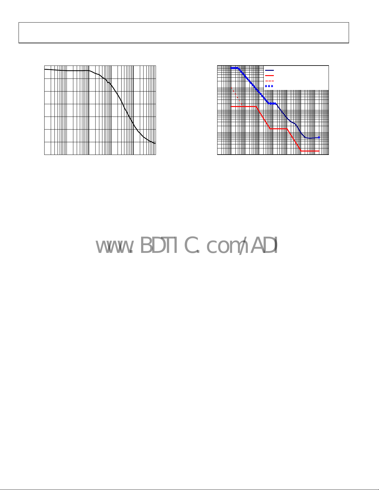
Figure 2. LOS Comparator Trip Point Programming
04228-0-003
0.1
1 10 100 1k 10k 100k 1M 10M
JITTER FREQUENCY (Hz)
Figure 3. Typical Measured Jitter Tolerance OC-48
100M
04228-0-030
Rev. PrA | Page 8 of 33
Preliminary Technical Data ADN2865
www.BDTIC.com/ADI
TIMING CHARACTERISTICS
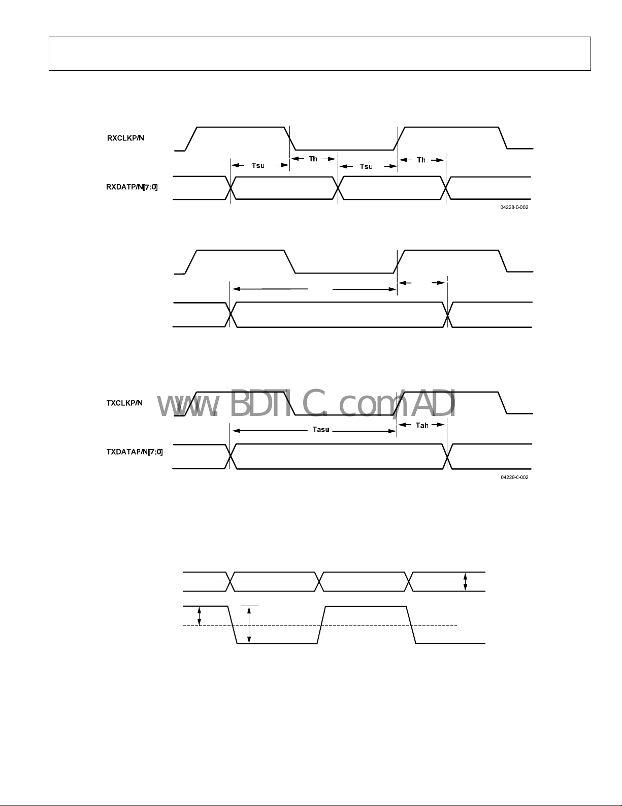
Figure 4. Rx Output Timing
/ N
RXCLKP
Tssu
TXDATAP
/ N [ 7 : 0 ]
Figure 5. Tx Input Timing (Sync Mode)
Figure 6. Tx Input Timing Align Mode)
Tsh
04228
-0-
002
OUTP
OUTN
OUTP–OUTN
V
CML
V
0V
SE
V
DIFF
Figure 75. Single-Ended vs. Differential Output Specifications
V
SE
04228-0-004
Rev. PrA | Page 9 of 33
ADN2865 Preliminary Technical Data
www.BDTIC.com/ADI
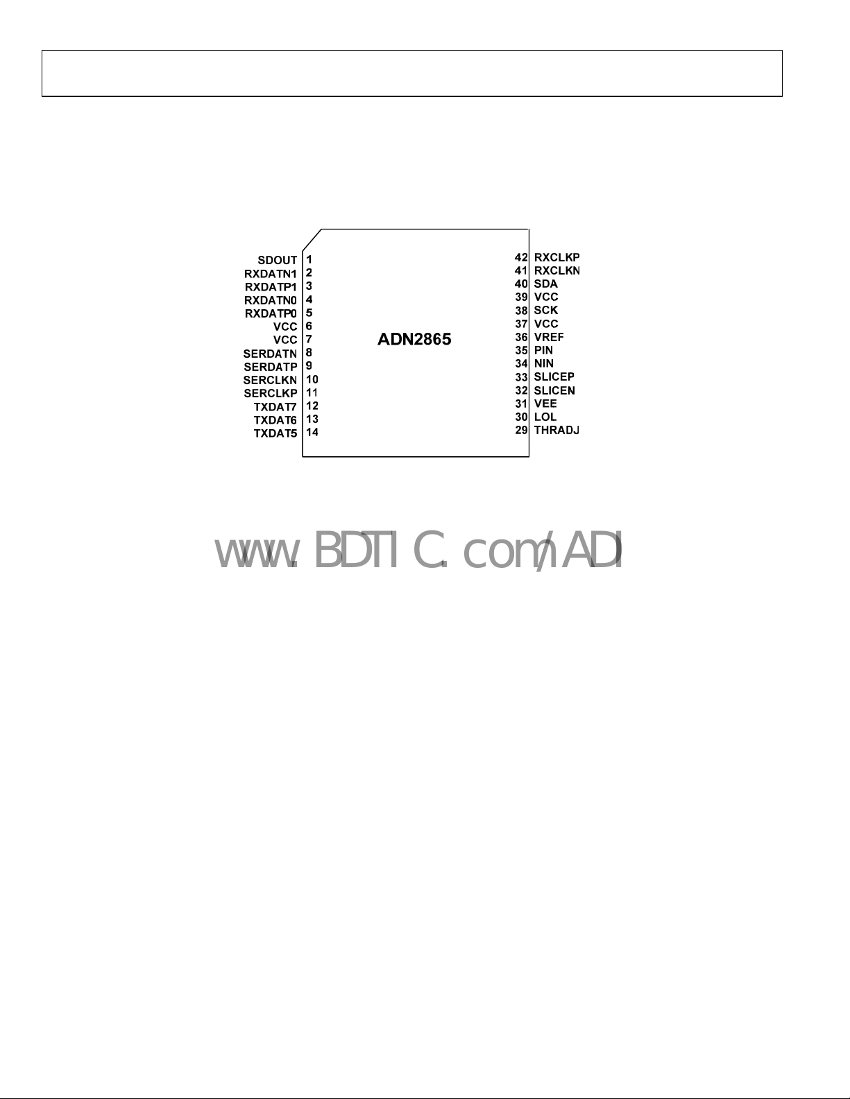
PIN CONFIGURATION AND FUNCTION DESCRIPTIONS
RXDATP2
RXDATN2
RXDATP3
RXDATN3
RXDATP4
RXDATN4
VCC
RXDATP5
RXDATN5
RXDATP6
RXDATN6
VCC
RXDATP7
RXDATN7
56555453525150494847464544
43
15161718192021222324252627
CF1
VEE
VEE
VCC
VCC
TXDAT2
TXDAT1
VREG
TXDAT0
TXCLK
TXDAT4
TXDAT3
Figure 86. Pin Configuration
REFN
28
REFP
Rev. PrA | Page 10 of 33
 Loading...