3 V Dual-Loop 50 Mbps to 1.25 Gbps
a
FEATURES
50 Mbps to 1.25 Gbps Operation
Single 3.3 V Operation
Bias Current Range 2 mA to 100 mA
Modulation Current Range 5 mA to 80 mA
Monitor Photo Diode Current 50 A to 1200 A
50 mA Supply Current at 3.3 V
Closed-Loop Control of Power and Extinction Ratio
Full Current Parameter Monitoring
Laser Fail and Laser Degrade Alarms
Automatic Laser Shutdown, ALS
Optional Clocked Data
Supports FEC Rates
32-Lead (5 mm × 5 mm) LFCSP Package
APPLICATIONS
SONET OC-1/3/12
SDH STM-0/1/4
Fibre Channel
Gigabit Ethernet
Laser Diode Driver
ADN2848
GENERAL DESCRIPTION
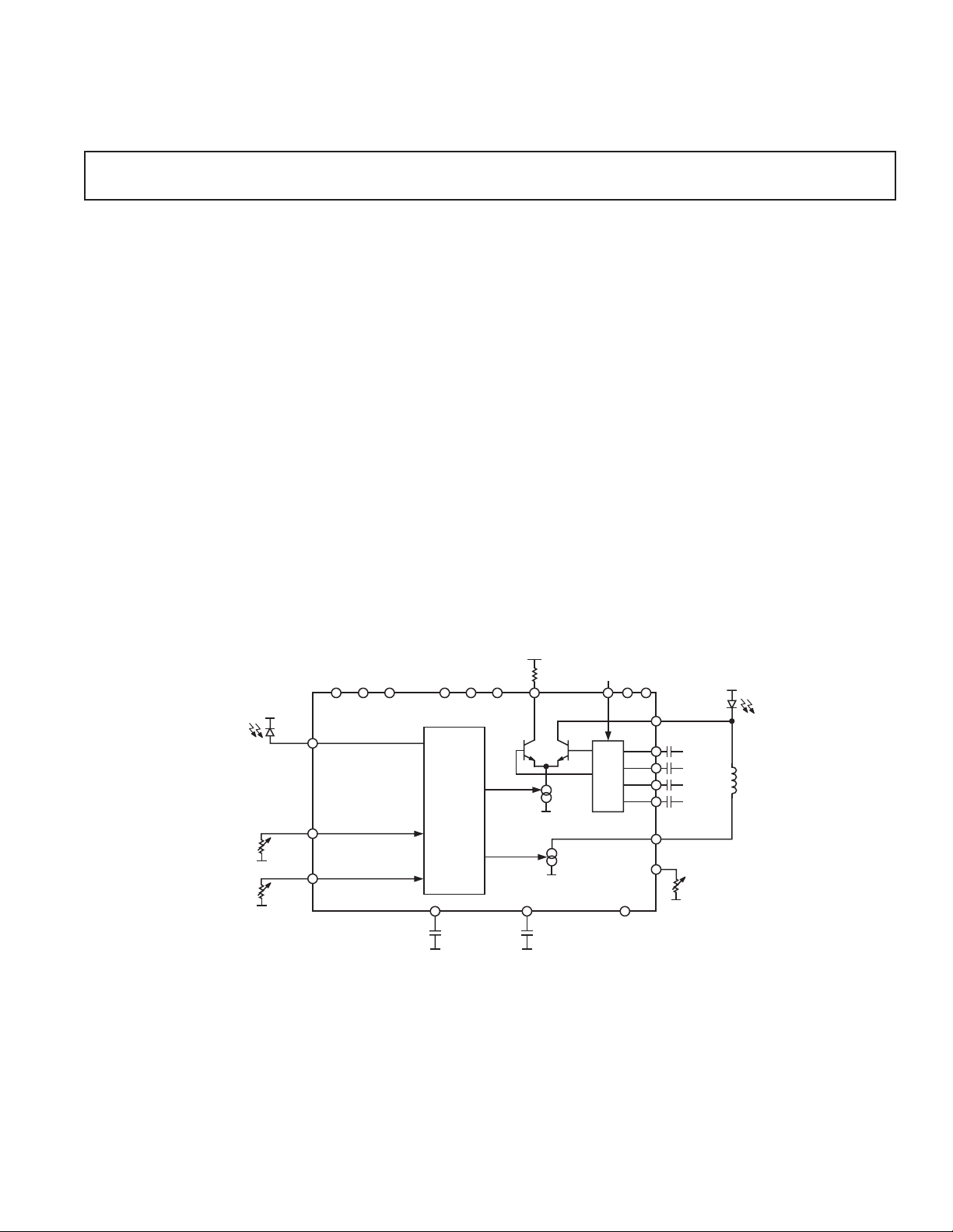
The ADN2848 uses a unique control algorithm to control both
the average power and extinction ratio of the laser diode, LD,
after initial factory setup. External component count and PCB
area are low as both power and extinction ratio control are
fully integrated. Programmable alarms are provided for laser fail
(end of life) and laser degrade (impending fail).
MPD
GND
GND
V
CC
IMPD
PSET
ERSET
FUNCTIONAL BLOCK DIAGRAM
V
CC
IBMON
IMMON
IMPDMON
ALS
CONTROL
FAIL
DEGRADE
I
MOD
I
BIAS
PAV CAPERCAP
GNDGND
IMODN
CLKSEL
ADN2848
LBWSET
CC
V
GND
IMODP
I
BIAS
ASET
GND
DATAP
DATAN
CLKP
CLKN
V
CC
LD
REV. 0
Information furnished by Analog Devices is believed to be accurate and
reliable. However, no responsibility is assumed by Analog Devices for its
use, nor for any infringements of patents or other rights of third parties that
may result from its use. No license is granted by implication or otherwise
under any patent or patent rights of Analog Devices. Trademarks and
registered trademarks are the property of their respective companies.
One Technology Way, P.O. Box 9106, Norwood, MA 02062-9106, U.S.A.
Tel: 781/329-4700 www.analog.com
Fax: 781/326-8703 © 2003 Analog Devices, Inc. All rights reserved.

1
ADN2848–SPECIFICATIONS
(VCC = 3.0 V to 3.6 V. All specifications T
Typical values as specified at 25C.)
MIN
to T
, unless otherwise noted.
MAX
Parameter Min Typ Max Unit Conditions/Comments
LASER BIAS (BIAS)
Output Current I
BIAS
Compliance Voltage 1.2 V
During ALS 0.1 mA
I
BIAS
ALS Response Time 5 sI
CCBIAS Compliance Voltage 1.2 V
2 100 mA
CC
CC
V
V
< 10% of nominal
BIAS
MODULATION CURRENT (IMODP, IMODN)
Output Current I
MOD
Compliance Voltage 1.5 V
I
During ALS 0.1 mA
MOD
Rise Time
Fall Time
Random Jitter
Pulsewidth Distortion
2
2
2
2
580mA
CC
V
80 170 ps
80 170 ps
1 1.5 ps RMS
15 ps I
= 40 mA
MOD
MONITOR PD (MPD)
Current 50 1200 AAverage Current
Compliance Voltage 1.65 V
POWER SET INPUT (PSET)
Capacitance 80 pF
Monitor Photodiode Current into RPSET Resistor 50 1200 AAverage Current
Voltage 1.1 1.2 1.3 V
EXTINCTION RATIO SET INPUT (ERSET)
Allowable Resistance Range 1.2 25 kΩ
Voltage 1.1 1.2 1.3 V
ALARM SET (ASET)
Allowable Resistance Range 1.2 25 kΩ
Voltage 1.1 1.2 1.3 V
Hysteresis 5 %
CONTROL LOOP Low Loop Bandwidth Selection
Time Constant 0.22 s LBWSET = GND
DATA INPUTS (DATAP, DATAN, CLKP, CLKN)
3
2.25 s LBWSET = V
CC
V p-p (Single-Ended, Peak-to-Peak) 100 500 mV Data and Clock Inputs Are
Input Impedance (Single-Ended) 50 Ω AC-Coupled
4
(see Figure 1) 50 ps
t
SETUP
4
t
(see Figure 1) 100 ps
HOLD
LOGIC INPUTS (ALS, LBWSET, CLKSEL)
V
IH
V
IL
2.4 V
0.8 V
ALARM OUTPUTS (Internal 30 kΩ Pull-Up)
V
OH
V
OL
2.4 V
0.8 V
IBMON, IMMON, IMPDMON
IMMON Division Ratio 100 A/A
IMPDMON 1 A/A
Compliance Voltage 0 VCC – 1.2 V
SUPPLY
5
I
CC
6
V
CC
NOTES
1
Temperature range is as follows: –40°C to +85°C.
2
Measured into a 25 Ω load using a 0-1 pattern at 622 Mbps.
3
When the voltage on DATAP is greater than the voltage on DATAN, the modulation current flows in the IMODP pin.
4
Guaranteed by design and characterization. Not production tested.
5
I
for power calculation on page 6 is the typical ICC given.
CCMIN
6
All VCC pins should be shorted together.
Specifications subject to change without notice.
3.0 3.3 3.6 V
50 mA I
BIAS
= I
MOD
= 0
REV. 0–2–

ADN2848
ABSOLUTE MAXIMUM RATINGS
(TA = 25°C, unless otherwise noted.)
VCC to GND . . . . . . . . . . . . . . . . . . . . . . . . . . . . . . . . . . 4.2 V
Digital Inputs
(ALS, LBWSET, CLKSEL) . . . . . . . . . –0.3 V to V
IMODN, IMODP . . . . . . . . . . . . . . . . . . . . . . . . . V
Operating Temperature Range
Industrial . . . . . . . . . . . . . . . . . . . . . . . . . . –40°C to +85°C
1
ORDERING GUIDE
Temperature Package
Model Range Description
+ 0.3 V
CC
+ 1.2 V
CC
ADN2848ACP-32 –40°C to +85°C 32-Lead LFCSP
ADN2848ACP-32-RL –40°C to +85°C 32-Lead LFCSP
ADN2848ACP-32-RL7 –40°C to +85°C 32-Lead LFCSP
Storage Temperature Range . . . . . . . . . . . . –65°C to +150°C
Junction Temperature (T
32-Lead LFCSP Package
Power Dissipation
Thermal Impedance3 . . . . . . . . . . . . . . . . . . . . . 32°C/W
θ
JA
max) . . . . . . . . . . . . . . . . . . . 150°C
J
2
. . . . . . . . . . . . . . . . (TJ max – TA)/θJA W
SETUP
t
S
Lead Temperature (Soldering for 10 sec) . . . . . . . . . . 300°C
NOTES
1
Stresses above those listed under Absolute Maximum Ratings may cause permanent damage to the device. This is a stress rating only; functional operation of the
device at these or any other conditions above those listed in the operational sections
of this specification is not implied. Exposure to absolute maximum rating conditions for extended periods may affect device reliability.
2
Power consumption formulae are provided on Page 6.
3
θ
is defined when device is soldered in a 4-layer board.
JA
DATAP/DATAN
CLKP
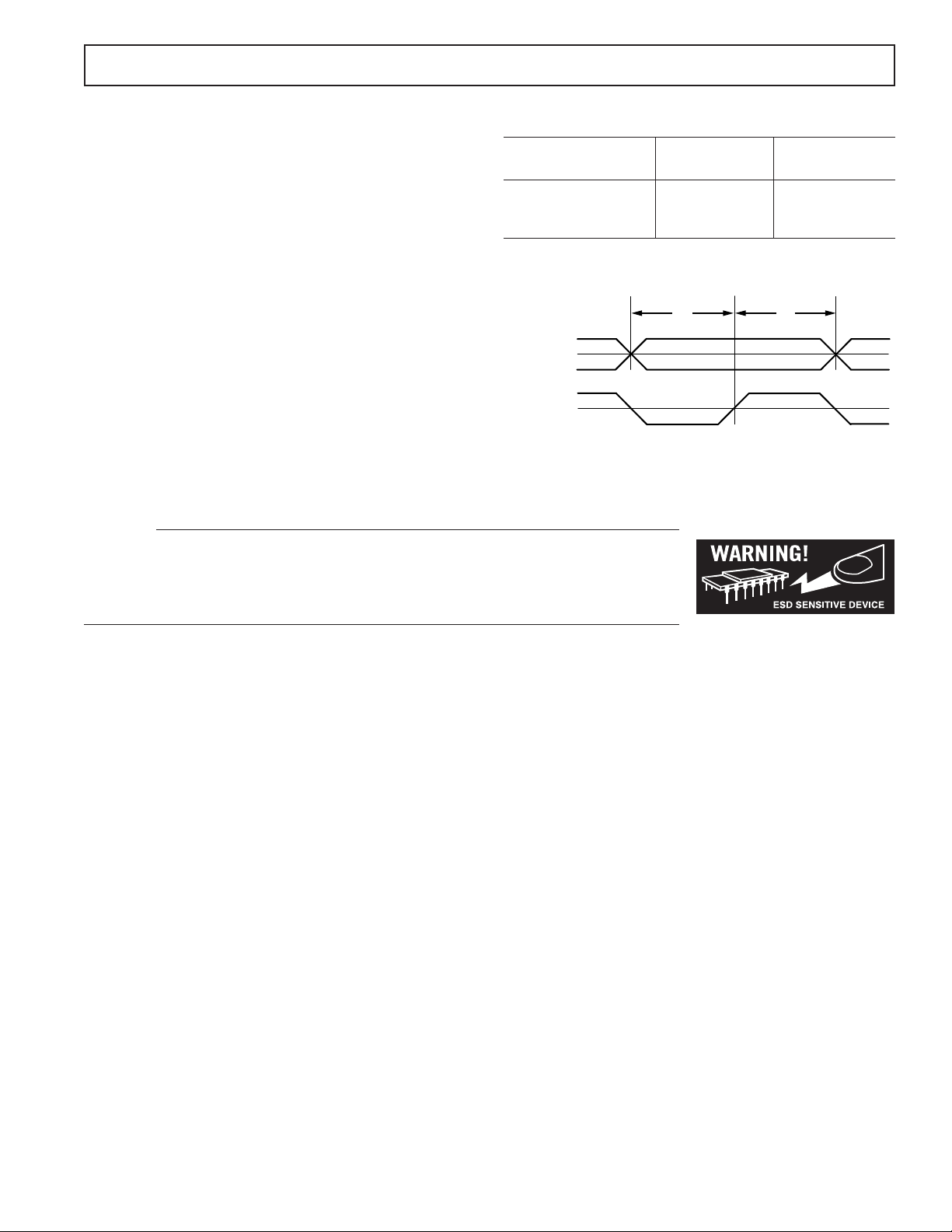
Figure 1. Setup and Hold Time
CAUTION
ESD (electrostatic discharge) sensitive device. Electrostatic charges as high as 4000 V readily
accumulate on the human body and test equipment and can discharge without detection. Although the
ADN2848 features proprietary ESD protection circuitry, permanent damage may occur on devices
subjected to high energy electrostatic discharges. Therefore, proper ESD precautions are recommended
to avoid performance degradation or loss of functionality.
HOLD
t
H
REV. 0
–3–

ADN2848
PIN CONFIGURATION
3
CC
20 ALS
19 FAIL
18 DEGRADE
21 V
IMPD 5
PSET 4
17 CLKSEL
4 8
CC
V
GND4 7
IMPDMON 6
16 CLKN
15 CLKP
14 GND1
13 DATAP
12 DATAN
1
11 V
CC
10 PAVCAP
9 ERCAP
CC
CC
CC
24 IBMON
23 IMMON
22 GND3
2 25
V
CC
IMODN 26
GND2 27
IMODP 28
GND2 29
GND2 30
31
I
BIAS
CCBIAS 32
ADN2848
TOP VIEW
ASET 2
ERSET 3
LBWSET 1
PIN FUNCTION DESCRIPTIONS
Pin Number Mnemonic Function
1 LBWSET Loop Bandwidth Select
2 ASET Alarm Threshold Set Pin
3 ERSET Extinction Ratio Set Pin
4 PSET Average Optical Power Set Pin
5 IMPD Monitor Photodiode Input
6IMPDMON Mirrored Current from Monitor Photodiode—Current Source
7 GND4 Supply Ground
8V
4 Supply Voltage
CC
9 ERCAP Extinction Ratio Loop Capacitor
10 PAVCAP Average Power Loop Capacitor
11 V
1 Supply Voltage
CC
12 DATAN Data Negative Differential Terminal
13 DATAP Data Positive Differential Terminal
14 GND1 Supply Ground
15 CLKP Data Clock Positive Differential Terminal, Used if CLKSEL = V
16 CLKN Data Clock Negative Differential Terminal, Used if CLKSEL = V
17 CLKSEL Clock Select (Active = VCC), Used if Data Is Clocked into Chip
18 DEGRADE DEGRADE Alarm Output
19 FAIL FAIL Alarm Output
20 ALS Automatic Laser Shutdown
21 V
3 Supply Voltage
CC
22 GND3 Supply Ground
23 IMMON Modulation Current Mirror Output—Current Source
24 IBMON Bias Current Mirror Output—Current Source
25 V
2 Supply Voltage
CC
26 IMODN Modulation Current Negative Output, Connect via Matching Resistor to V
27 GND2 Supply Ground
28 IMODP Modulation Current Positive Output, Connect to Laser Diode
29 GND2 Supply Ground
30 GND2 Supply Ground
31 I
BIAS
Laser Diode Bias Current Output
32 CCBIAS Extra Laser Diode Bias When AC-Coupled—Current Sink
REV. 0–4–
 Loading...