ANALOG DEVICES ADN2847 Service Manual

3.3 V Dual-Loop 50 Mbps to 3.3 Gbps
Data Sheet
FEATURES
50 Mbps to 3.3 Gbps operation
Single 3.3 V operation
Typical rise/fall time: 80 ps
Bias current range: 2 mA to 100 mA
Modulation current range: 5 mA to 80 mA
Monitor photodiode current: 50 μA to 1200 μA
Dual MPD functionality for DWDM
50 mA supply current at 3.3 V
Closed-loop control of power and extinction ratio
Full current parameter monitoring
Laser fail and laser degrade alarms
Automatic laser shutdown (ALS)
Optional clocked data
Supports FEC rates
48-lead (7 mm × 7 mm) LFCSP package
32-lead (5 mm × 5 mm) LFCSP package
Laser Diode Driver
ADN2847
APPLICATIONS
SONET OC-1/3/12/48
SDH STM-0/1/4/16
Fibre Channel
Gigabit Ethernet
DWDM dual MPD wavelength control
GENERAL DESCRIPTION
The ADN2847 uses a unique control algorithm to control both
average power and extinction ratio of the laser diode (LD) after
initial factory setup. External component count and PCB area
are low, as both power and extinction ratio control are fully
integrated. Programmable alarms are provided for laser fail
(end of life) and laser degrade (impending fail).
Optional dual MPD current monitoring is designed into the
ADN2847 specifically for DWDM wavelength control.
The ADN2847 is specified for the −40°C to +85°C temperature
range and is available in a 48-lead LFCSP package and a 32-lead
LFCSP package.
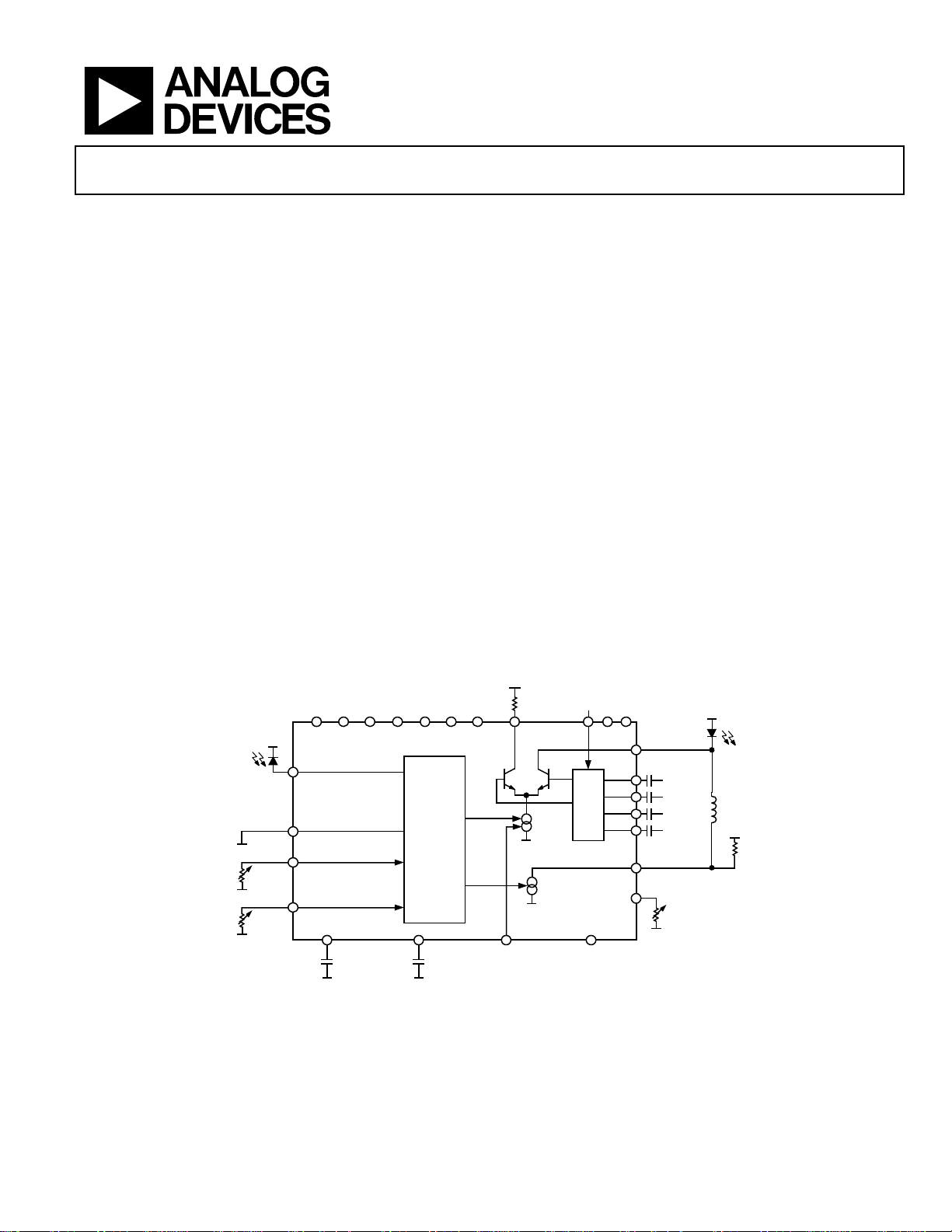
FUNCTIONAL BLOCK DIAGRAM
V
CC
CLKSEL
MPD
GND
GND
GND
V
CC
IMPD
IMPD2
PSET
ERSET
IBMON
IMMON
IMPDMON
IMPDMON2
CONTROL
PAV C A PERCAP
GNDGND
CC
ALS
FAI L
DEGRADE
IMODN
I
MOD
I
BIAS
V
GND
IMODP
I
BIAS
ASET
ADN2847
GND
LBWSETIDTONE
Figure 1.
DATAP
DATAN
CLKP
CLKN
LD
V
CC
V
CC
R
Z
02745-001
Rev. B
Information furnished by Analog Devices is believed to be accurate and reliable. However, no
responsibility is assumed by Anal og Devices for its use, nor for any infringements of patents or ot her
rights of third parties that may result from its use. Specifications subject to change without notice. No
license is granted by implication or otherwise under any patent or patent rights of Analog Devices.
Trademarks and registered trademarks are the property of their respective owners.
One Technology Way, P.O. Box 9106, Norwood, MA 02062-9106, U.S.A.
Tel: 781.329.4700 www.analog.com
Fax: 781.461.3113 ©2003–2012 Analog Devices, Inc. All rights reserved.

ADN2847 Data Sheet
TABLE OF CONTENTS
Features.............................................................................................. 1
Applications....................................................................................... 1
General Description ......................................................................... 1
Functional Block Diagram .............................................................. 1
Revision History ............................................................................... 2
Specifications..................................................................................... 3
Timing Diagrams.......................................................................... 4
Absolute Maximum Ratings............................................................ 5
Thermal Resistance ...................................................................... 5
ESD Caution.................................................................................. 5
Die Pad Coordinates ........................................................................ 6
Pin Configurations and Function Descriptions ........................... 7
Theory of Operation ........................................................................ 9
Control........................................................................................... 9
Loop Bandwidth Selection .......................................................... 9
Alarms.............................................................................................9
Monitor Currents ....................................................................... 10
Dual MPD DWDM Function (48-Lead LFCSP Only) ......... 10
IDTONE (48-Lead LFCSP Only)............................................. 10
Data and Clock Inputs............................................................... 10
CCBIAS........................................................................................ 10
I
................................................................................................ 10
BIAS
Automatic Laser Shutdown....................................................... 10
Alarm Interfaces......................................................................... 11
Power Consumption .................................................................. 11
Laser Diode Interfacing............................................................. 11
Optical Supervisor...................................................................... 11
Outline Dimensions....................................................................... 14
Ordering Guide .......................................................................... 15
REVISION HISTORY
3/12—Rev. A to Rev. B
Added EPAD Notation .................................................................... 7
Updated Outline Dimensions....................................................... 14
Changes to Ordering Guide.......................................................... 15
10/06—Rev. 0 to Rev. A
Updated Format..................................................................Universal
Change to Data Sheet Title.............................................................. 1
Changes to Figure 1.......................................................................... 1
Changes to Specifications................................................................ 3
Added I
Changes to Laser Diode Interfacing Section............................... 11
Changes to Figure 14...................................................................... 12
Changes to Figure 15...................................................................... 13
Changes to Ordering Guide.......................................................... 15
1/03—Revision 0: Initial Version
Section ......................................................................... 10
BIAS
Rev. B | Page 2 of 16

Data Sheet ADN2847
SPECIFICATIONS
VCC = 3.0 V to 3.6 V. Temperature range: −40°C to +85°C. All specifications T
at T
= 25°C.
A
Table 1.
Parameter Min Typ Max Unit Conditions/Comments
LASER BIAS CURRENT (I
Output Current I
I
when ALS is asserted 0.1 mA
BIAS
, ALS)
BIAS
2 100 mA
BIAS
ALS Assertion Time 5 μs I
I
Compliance Voltage 1.2 VCC V
BIAS
CCBIAS Compliance Voltage 1.2 VCC V
MODULATION CURRENT (IMODP, IMODN)1
Output Current I
5 80 mA
MOD
Compliance Voltage 1.5 VCC V
I
when ALS is Asserted 0.1 mA
MOD
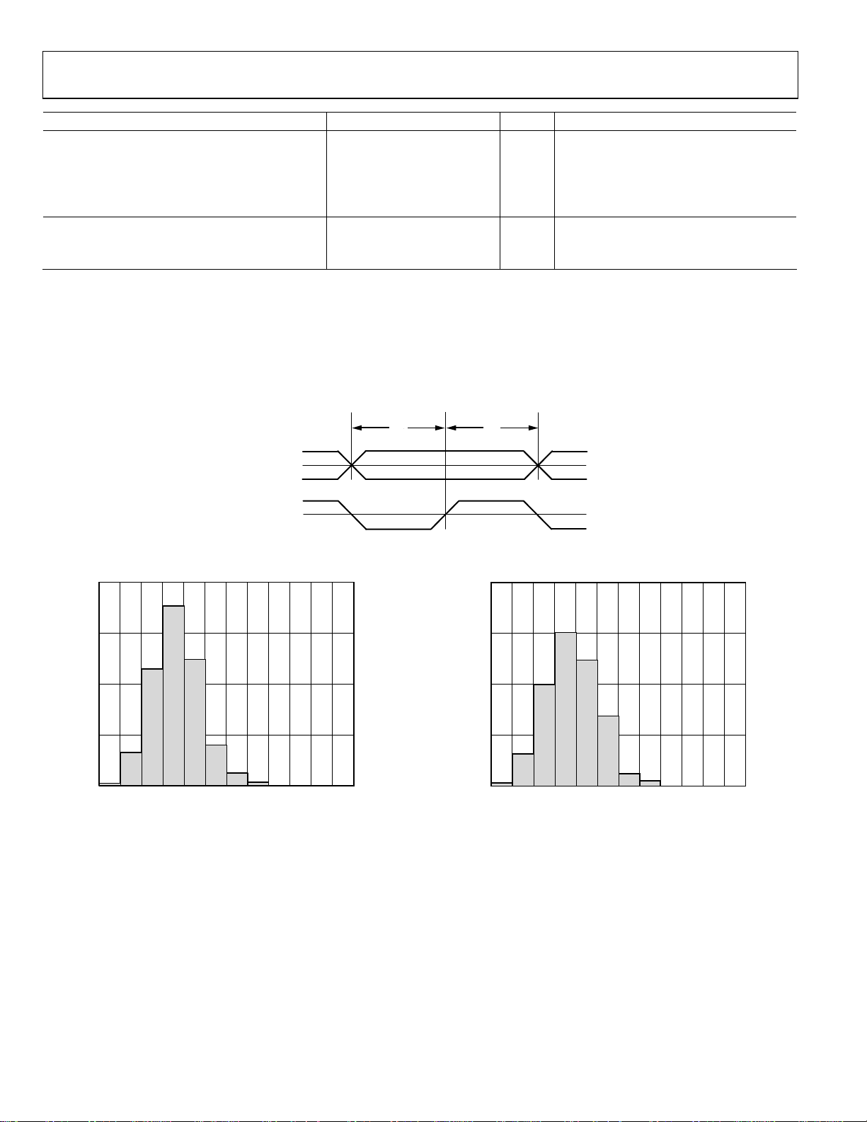
Rise Time2 80 120 ps See Figure 3 for device rise time histogram
Fall Time2 80 120 ps See Figure 4 for device fall time histogram
Random Jitter2 1 1.5 ps RMS
Pulse Width Distortion2 15 ps I
MONITOR PD (MPD, MPD2)
Current 50 1200 μA Average current
Compliance Voltage 1.65 V
POWER SET INPUT (PSET)
Capacitance 80 pF
Monitor Photodiode Current into RPSET Resistor 50 1200 μA Average current
Voltage 1.1 1.2 1.3 V
EXTINCTION RATIO SET INPUT (ERSET)
Allowable Resistance Range 1.2 25 kΩ
Voltage 1.1 1.2 1.3 V
ALARM SET (ASET)
Allowable Resistance Range 1.2 25 kΩ
Voltage 1.1 1.2 1.3 V
Hysteresis 5 %
CONTROL LOOP Low Loop Bandwidth selection
Time Constant 0.22 sec LBWSET = GND
2.25 sec LBWSET = VCC
DATA INPUTS (DATAP, DATAN, CLKP, CLKN)3
V p-p (Single-Ended, Peak-to-Peak) 100 500 mV Data and clock inputs are ac-coupled
Input Impedance (Single-Ended) 50 Ω
4
t
50 ps See Figure 2
SETUP
4
t
100 ps See Figure 2
HOLD
LOGIC INPUTS (ALS, LBWSET, CLKSEL)
VIH 2.4 V
VIL 0.8 V
ALARM OUTPUTS (FAIL, DEGRADE) Internal 30 kΩ Pull-Up
V
2.4 V
OH
VOL 0.8 V
IDTONE
Compliance Voltage VCC − 1.5 V
I
Ratio 2
OUT/IIN
5
f
0.01 1 MHz
IN
MIN
to T
, unless otherwise noted. Typical values specified
MAX
< 10% of nominal
BIAS
= 40 mA
MOD
User to supply current sink in the range of
50 μA to 4 mA
Rev. B | Page 3 of 16

ADN2847 Data Sheet
Parameter Min Typ Max Unit Conditions/Comments
IBMON, IMMON, IMPDMON, IMPDMON2
IBMON, IMMON Division Ratio 100 A/A
IMPDMON, IMPDMON2 1 A/A
IMPDMON to IMPDMON2 Matching 2 % I
Compliance Voltage 0 VCC −1.2 V
SUPPLY
6
I
50 mA I
CC
7
V
3.0 3.3 3.6 V
CC
1
The high speed performance for the die version of ADN2847 can be achieved when using the bonding diagram shown in Figure 6.
2
Measured into a 25 Ω load using a 11110000 pattern at 2.5 Gbps.
3
When the voltage on DATAP is greater than the voltage on DATAN, the modulation current flows in the IMODP pin.
4
Guaranteed by design and characterization. Not production tested.
5
IDTONE can cause eye distortion.
6
I
for power calculation in the P section is the typical ICC given. ower Consumption
CCMIN
7
All VCC pins should be shorted together.
TIMING DIAGRAMS
= 1200 μA
MPD
= I
BIAS
MOD
= 0
DA TAP/ D ATAN
CLKP
40
30
20
COUNT (%)
10
0
76
78 82 84 86 88 90 92 94 96 98 10080
RISE TIME (ps)
Figure 3. Rise Time Distribution Under Worst-Case Operating Conditions
SETUP
t
S
Figure 2. Setup and Hold Time
40
30
20
COUNT (%)
10
2745-007
Figure 4. Fall Time Distribution Under Worst-Case Operating Conditions
HOLD
t
H
0
80
82 86 88 90 92 94 96 98 100 102 10484
02745-002
FAL L TI ME ( p s )
02745-008
Rev. B | Page 4 of 16

Data Sheet ADN2847
ABSOLUTE MAXIMUM RATINGS
TA = 25°C, unless otherwise noted.
Table 2.
Parameter Rating
VCC to GND 4.2 V
Digital Inputs (ALS, LBWSET, CLKSEL) −0.3 V to VCC + 0.3 V
IMODN, IMODP V
Operating Temperature Range Industrial −40°C to +85°C
Storage Temperature Range −65°C to +150°C
Junction Temperature (TJ max) 150°C
Power Dissipation1 (W)
Lead Temperature (Soldering 10 sec) 300°C
1
Power consumption formulae are provided in the Power Consumption
section.
+ 1.2 V
CC
(TJ max − TA)/ θJA
THERMAL RESISTANCE
θJA is specified for the worst-case conditions, that is, a device
soldered in a circuit board for surface-mount packages.
Table 3. Thermal Resistance
Package Type θJA Unit
48-lead LFCSP 25 °C/W
32-lead LFCSP 32 °C/W
ESD CAUTION
Stresses above those listed under Absolute Maximum Ratings
may cause permanent damage to the device. This is a stress
rating only; functional operation of the device at these or any
other conditions above those indicated in the operational
section of this specification is not implied. Exposure to absolute
maximum rating conditions for extended periods may affect
device reliability.
Rev. B | Page 5 of 16
 Loading...