

a
10.709 Gbps High Speed Data Switch
ADN2845
FEATURES
Data Rates from 9.952 Gbps to 10.709 Gbps
Typical Rise/Fall Time 25 ps/23 ps
Bias Current Range 3 mA to 80 mA
Modulation Current Range 5 mA to 80 mA
Automatic Laser Shutdown, ALS
CML Data Inputs
50 Internal Data Terminations
3.3 V Single-Supply Operation
Driver Supplied in Die Format Only
APPLICATIONS
SONET OC-192, SDH STM-64
Supports 10.667 Gbps and 10.709 Gbps FEC Rates
10 Gb Ethernet IEEE802.3ae
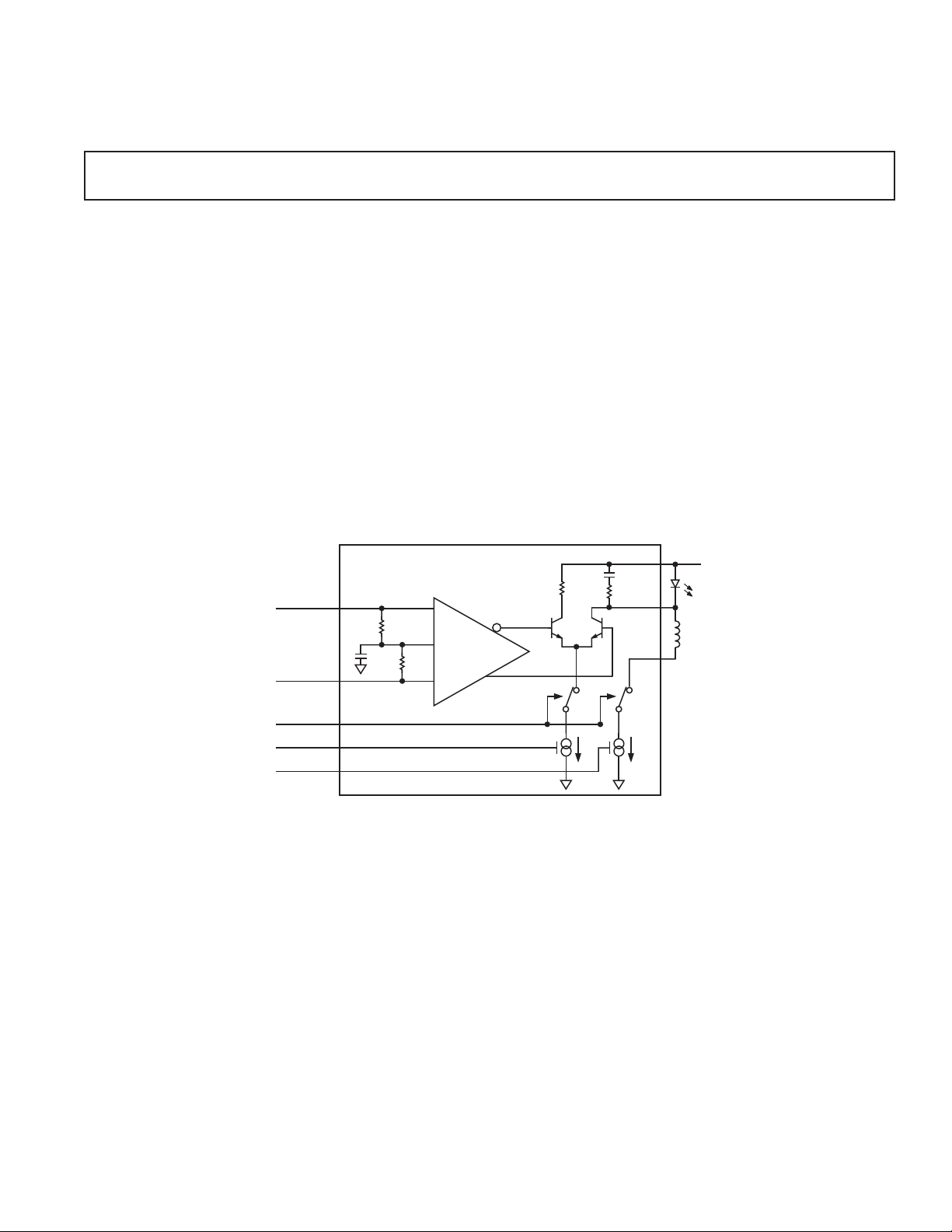
FUNCTIONAL BLOCK DIAGRAM
ADN2845
DATAP
50
DATAN
50
GENERAL DESCRIPTION
The ADN2845 is a 10.709 Gbps laser diode driver. The
ADN2845 eliminates the need to ac-couple since it can deliver
80 mA of modulation while dc-coupled to the laser diode. It is
intended to be copackaged with the laser to minimize bond
lengths, which improves performance of the optical transmitter.
The ADN2845 may be used in conjunction with the ADN2844
control chip. This chipset (ADN2843) offers a unique control
algorithm to control both average power and extinction ratio of
the laser diode.
For transmission line applications, contact the HSN Applications
Group at fiberoptic.ic@analog.com
V
CC
LD
IMODP
IBIAS
ALS
IMOD_CTRL
IBIAS_CTRL
REV. 0
Information furnished by Analog Devices is believed to be accurate and
reliable. However, no responsibility is assumed by Analog Devices for its
use, nor for any infringements of patents or other rights of third parties that
may result from its use. No license is granted by implication or otherwise
under any patent or patent rights of Analog Devices. Trademarks and
registered trademarks are the property of their respective companies.
One Technology Way, P.O. Box 9106, Norwood, MA 02062-9106, U.S.A.
Tel: 781/329-4700 www.analog.com
Fax: 781/326-8703 © 2003 Analog Devices, Inc. All rights reserved.
ADN2845-SPECIFICATIONS
(V
= 3.0 V to 3.6 V. All specifications T
ELECTRICAL CHARACTERISTICS
CC
as specified at 25ⴗC.)
Parameter Min Typ Max Unit Conditions
LASER BIAS (BIAS)
Output Current I
BIAS
380mA
Compliance Voltage 1.2 V
during ALS 10 ASee Note 1
I
BIAS
ALS Shutdown Response Time 10 s
MODULATION CURRENT (LMODP, IMODN) See Note 2
Output Current I
MOD
580mA
Compliance Voltage 1.2 V
during ALS 10 A
I
MOD
Rise Time 25 ps
Fall Time 23 ps
Random Jitter 170 fs rms See Note 3
Total Jitter 7.41 ps p-p See Note 4
DATA INPUTS (DATAP, DATAN)
V p-p(Single-Ended Peak-to-Peak) 300 800 mV
Input Impedance 50
LOGIC INPUTS (ALS)
V
IH
V
IL
2.4 V
0.8 V
IMOD_CTRL Input See Note 5
Gain (IMOD_CTRL to I
)1015.5 A/A
MOD
Input Voltage 1.5 V
IBIAS_CTRL Input See Note 5
Gain (IBIAS_CTRL to I
)912A/A
BIAS
Input Voltage 1.5 V
SUPPLY
V
CC
I
CC
NOTES
1
In ALS mode, approximately 15 mA is sourced to the laser from the IBIAS pin, which reverse biases the laser.
2
The ADN2845 high speed specifications are measured into a 5 load.
3
RMS jitter measured with a 0000 0000 1111 1111 repeating pattern at 10.7 Gbps rate.
4
Peak-to-peak total jitter measured with a 2
5
It is recommended to decouple these pins to VCC rather than GND.
6
IBIAS = 0, IMOD = 0 (when ALS is asserted). See Power Dissipation section on page 4 for calculation of complete power dissipation.
Specifications subject to change without notice.
13
– 1 PRBS pattern with 80 CIDs input pattern at 10.7 Gbps rate.
3.0 3.3 3.6 V
75 mA See Note 6
to T
MIN
–1.0 V
CC
CC
, unless otherwise noted. Typical values
MAX
V
ABSOLUTE MAXIMUM RATINGS*
(TA = 25°C, unless otherwise noted.)
VCC to GND . . . . . . . . . . . . . . . . . . . . . . . . . . . . . . . . . . . . 5 V
DATAP to GND . . . . . . . . . . . . . . . . . . . . . . . –0.5 V to 4.2 V
DATAN to GND . . . . . . . . . . . . . . . . . . . . . . –0.5 V to 4.2 V
ALS to GND . . . . . . . . . . . . . . . . . . . . . . . . . . –0.5 V to 4.2 V
IMOD_CONTROL to GND . . . . . . . . . . . . . –0.5 V to 4.2 V
IBIAS_CONTROL to GND . . . . . . . . . . . . . . –0.5 V to 4.2 V
IMODN, IMODP . . . . . . . . . . . . . . . . . . . . . . . . . V
+1.2 V
CC
Operating Temperature Range
Industrial . . . . . . . . . . . . . . . . . . . . . . . . . . . –40°C to +85°C
Storage Temperature Range . . . . . . . . . . . . . –65°C to +150°C
Junction Temperature (T
*Stresses above those listed under Absolute Maximum Ratings may cause perma-
nent damage to the device. This is a stress rating only; functional operation of the
device at these or any other conditions above those indicated in the operational
section of this specification is not implied. Exposure to absolute maximum rating
conditions for extended periods may affect device reliability.
max) . . . . . . . . . . . . . . . . . . . 150°C
J
ORDERING GUIDE
Temperature Package Qty.
Model Range Description Min.
ADN2845ACHIPS –40ºC to +85ºC Die Form 100
REV. 0–2–
ADN2845
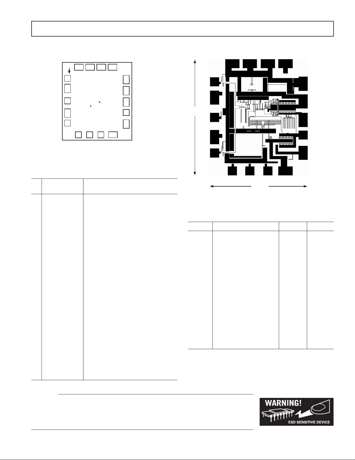
PIN CONFIGURATION
DATAN
GND
GND
DATAP
CC
V
1
PAD PITCH: 200m
NC
DIE SIZE: 1140m ( 20m)
ⴛ 1340m (
DIE THICKNESS: 0.25mm
SINGLE PAD SIZE: 92m ⴛ 92m
DOUBLE PAD SIZE: 151m ⴛ 92m
ALS
VCCV
ADN2845
20m)
IMOD_CTRL
CC
GND
GND
IBIAS_CTRL
V
CC
(IMODN TERM)
NC
IMODP
IBIAS
NC
PIN FUNCTION DESCRIPTIONS
Pin
No. Mnemonic Function
1 DATAN AC-Coupled CML Data, Negative
Differential Terminal
2GND Negative Supply
3NCNo Connect. Leave floating.
4GND Negative Supply
5 DATAP AC-Coupled CML Data, Positive
Differential Terminal
6 ALS Automatic Laser Shutdown Logic Input
7IMOD_CTRL Modulation Current Control Input
(Control circuit sinks IMOD/10 from
pin to GND.)
8IBIAS_CTRL BIAS Current Control Input (Control
circuit sinks IBIAS/10 from pin to GND.)
9GND Negative Supply
10 NC No Connect. Leave floating.
11 IBIAS BIAS Current
12 IMODP Modulation Current
13 NC No Connect. Leave floating.
14 V
CC
VCC Connection for IMODN
Termination Resistor
15 GND Negative Supply
16 V
17 V
18 V
CC
CC
CC
Positive Supply
Positive Supply
Positive Supply
METALLIZATION PHOTOGRAPH
GNDV
V
CC
V
CC
(IMODN TERM)
NC
IMODP
IBIAS
NC
GNDIBIAS_CTRLALS IMOD_CTRL
1
DATAN
1340m
(ⴞ20m)
DATAP
GND
NC
GND
V
CC
CC
1140m
(ⴞ20m)
DIE PAD COORDINATES
Pad No. Pad Name X (m) Y (m)
1 DATAN –500.00 400.00
2 GND
3NC –500.00 0.00
4 GND
2
2
–500.00 222.00
–500.00 –222.00
5 DATAP –500.00 –400.00
6 ALS –300.00 –600.00
7IMOD_CTRL –100.00 –600.00
8IBIAS_CTRL 100.00 –600.00
9 GND
10 NC
11 IBIAS 500.00 –200.00
12 IMODP
13 NC
14 V
15 GND
16 V
17 V
18 V
NOTES
1
The reference point with x = 0, y = 0 is the center of the die.
2
Denotes double bond pad.
2
2
2
2
(IMODN TERM)2500.00 378.00
CC
2
2
CC
2
CC
2
CC
300.00 –600.00
500.00 –400.00
500.00 –30.00
500.00 178.00
300.00 600.00
100.00 600.00
–100.00 600.00
–300.00 600.00
CAUTION
ESD (electrostatic discharge) sensitive device. Electrostatic charges as high as 4000 V readily
accumulate on the human body and test equipment and can discharge without detection. Although the
ADN2845 features proprietary ESD protection circuitry, permanent damage may occur on devices
subjected to high energy electrostatic discharges. Therefore, proper ESD precautions are recommended
to avoid performance degradation or loss of functionality.
REV. 0
–3–

ADN2845
GENERAL
The ADN2845 is a 3.3 V high speed data switch that is
intended to be dc-coupled with a copackaged laser diode.
Achieving best performance requires using low inductance ribbon
connections between the ADN2845 and the laser.
IMOD__CRTL, IBIAS_CTRL
The operation of the ADN2845 is controlled by the two input
pins called IBIAS_CTRL and IMOD_CTRL. The user should
connect current sinks from each of these pins to GND.
These currents are internally mirrored and used to control the
actual values for the bias and modulation currents used to drive
the laser diode. It is recommended to decouple these pins to
VCC instead of GND.
DATA INPUTS
Figure 1 shows a simplified schematic of the ADN2845 data
inputs. The data inputs are terminated via the equivalent of a
100 internal resistor between DATAN and DATAP. This
provides 50 termination for single-ended signals. The actual
signal on the switching devices is attenuated by a factor of 2
internally. There is a high impedance circuit to set the commonmode voltage, which is designed to change over temperature. It
is recommended that ac coupling be used to eliminate the need
for matching between the common-mode voltages.
LASER SHUTDOWN
The ADN2845 ALS allows compliance to ITU-T-G958 (11/94),
section 9.7. When ALS is asserted, both bias and modulation
currents are turned off. In ASL mode, approximately 15 mA is
sourced to the laser from the IBIAS pin, which reverse biases
the laser and ensures that it is turned off. ALS should have a
10 kW pull-down resistor connected and should be driven with
correct logic levels (see Specifications section). The ALS pin
should never be left floating.
POWER DISSIPATION
The power dissipation of the ADN2845 can be calculated using
the following expressions:
ImAImAImA
=+¥ +¥75 1 75 0 3.().()
CC MOD BIAS
IA
()
PV I A V
=¥ + ¥ + ¥()
CC CC IMOD
where V
V
IBIAS
is the average voltage on the IMOD pin, and
IMOD
is the average voltage on the IBIAS pin.
MOD
VIA
2
IBIAS BIAS
()
DATAN
DATAP
25
25
25
25
2k
ADN2845
INTERNAL
REFERENCE
Figure 1. Simplified Schematic of the Data Inputs
V
V
CC
CC
VCCV
10nF
CC
GND
1518
IMODNTERM
14
10nF
DATAN
GND
10nF
CC
V
1
ADN2845
GND
10nF
DATAP
5
10k
6
ALS
V
IMOD_CTRL
CC
IBIAS_CTRL
10nF10nF
V
10
9
GND
CC
Figure 2. ADN2845 Application Circuit
V
CC
10F
TANTALUM
V
CC
10nF
IMODP
IBIAS
V
CC
LD
REV. 0–4–

ADN2845
PARALLEL PLATE
DECOUPLING
CAPACITOR
GROUND PLANE
MPD
50 TRANSMISSION LINE
GROUND PLANE
18 15
V
V
CC
CC
DATAN
1
AGND
ADN2845
AGND
DATAP
5
AGNDV
CC
IMODNTERM
BACK FACET LIGHT
14
V
CC
IMODP
IBIAS
10
AGNDALS IMOD_CTRL IBIAS_CTRL
96
IBIAS OUTPUT INDUCTOR
PARALLEL PLATE
DECOUPLING
CAPACITORS
CERAMIC WITH GOLD
SURFACE THAT CONTACTS
THE LASER’S ANODE
LASER LIGHT
LASER
NOTES
• FOR OPTIMUM PERFORMANCE, RIBBON BONDS ARE RECOMMENDED ON PADS 1, 5, 1 2, AND 14 . WIRES ARE 3 MIL OR 5 MIL RIBBONS <400m
• LONG. ALL OTHER PINS CAN BE ROUND WIRE <1mm.
• LASER’S ANODE IS CONNECTED TO V
• 12 AND PAD 14 RIBBONS.
• PARALLEL PLATE DECOUPLING CAPACITORS SHOULD BE >100pF AND BE OF MICROWAVE AVX TYPE, PART NO. GB0159391KA6N (390pF).
• THE RECOMMENDED SUBSTRATE CONNECTION IS TO GND. HOWEVER, PERFORMANCE IS NOT AFFECTED BY CONNECTING THE
• SUBSTRATE TO VCC.
• AN INDUCTOR SHOULD BE USED IN THE BIAS CURRENT PATH. A MICROWAVE COMPONENTS COIL 30-1847-GCCAS-01 (48 MIL 24 MIL)
SHOULD BE USED.
• THE EXTERNAL POWER SUPPLY IS CONNECTED AT THE PARALLEL PLATE DECOUPLING CAPACITOR.
THROUGH GOLD LAYER ON TOP OF CERAMIC STANDOFF. STANDOFF MINIMIZES LENGTH OF PAD
CC
Figure 3. Recommended Layout
REV. 0
Figure 4. 10 Gbps Optical Diagram Provided Courtesy of NEL.
P
= 0 dBm, ER = 5 dB, PRBS 31 Pattern.
AV
–5–

ADN2845
OUTLINE DIMENSIONS
18-Pad Bare Die
Dimensions shown in micrometers and millimeters
1
ADN2845
PAD PITCH: 200m
DIE SIZE: 1140m (20m)
1340m (20m)
DIE THICKNESS: 0.25mm
SINGLE PAD SIZE: 92m 92m
DOUBLE PAD SIZE: 151m 92m
1140m (20m)
0.25 mm
1340m (20m)
REV. 0–6–

–7–

C03082–0–4/03(0)
–8–
 Loading...