

Dual-Loop 50 Mbps–2.7 Gbps
a
FEATURES
50 Mbps to 2.7 Gbps Operation
Typical Rise/Fall Time 80 ps
Bias Current Range 2 to 100 mA
Modulation Current Range 5 to 80 mA
Monitor Photodiode Current 50 A to 1200 A
Closed-Loop Control of Power and Extinction Ratio
Laser Fail and Laser Degrade Alarms
Automatic Laser Shutdown, ALS
Dual MPD Functionality for DWDM
Optional Clocked Data
Full Current Parameter Monitoring
5 V Operation
48-Lead LFCSP Package
32-Lead LFCSP Package (Reduced Functionality)
APPLICATIONS
DWDM Dual MPD Wavelength Fixing
SONET OC-1/3/12/48
SDH STM-1/4/16
Fibre Channel
Gigabit Ethernet
Laser Diode Driver
ADN2841
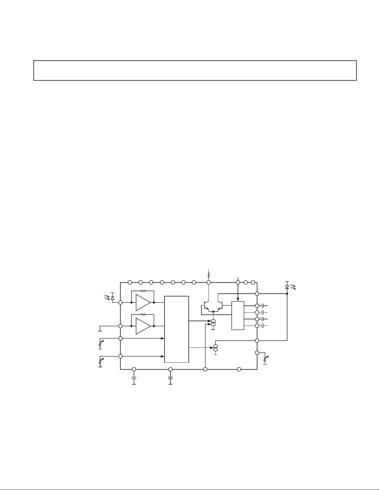
GENERAL DESCRIPTION
The ADN2841 uses a unique control algorithm to control both
the average power and extinction ratio of the laser diode (LD)
after initial factory setup. External component count and PCB area
are low, since both power and extinction ratio control are fully
integrated. Programmable alarms are provided for laser fail (end
of life) and laser degrade (impending fail).
The ADN2841 has circuitry for a second monitor photodiode,
which enables DWDM wavelength control.
MPD
GND
GND
GND
V
CC
IMPD
IMPD2
PSET
ERSET
FUNCTIONAL BLOCK DIAGRAM
V
IBMON
IMMON
IMPDMON
IMPDMON2
ALS
FAIL
DEGRADE
I
MOD
CONTROL
I
BIAS
PAV CAPERCAP
GNDGND
CC
IMODN
CLKSEL
ADN2841
LBWSETIDTONE
CC
V
GND
IMODP
IBIAS
ASET
GND
DATAP
DATAN
CLKP
CLKN
V
CC
LD
REV. A
Information furnished by Analog Devices is believed to be accurate and
reliable. However, no responsibility is assumed by Analog Devices for its
use, nor for any infringements of patents or other rights of third parties that
may result from its use. No license is granted by implication or otherwise
under any patent or patent rights of Analog Devices.
One Technology Way, P.O. Box 9106, Norwood, MA 02062-9106, U.S.A.
Tel: 781/329-4700 www.analog.com
Fax: 781/326-8703 © Analog Devices, Inc., 2002

ADN2841–SPECIFICATIONS
(VCC = 5 V 10%. All specifications T
values as specified at 25C.)
MIN
to T
, unless otherwise noted1. Typical
MAX
Parameter Min Typ Max Unit Conditions/Comments
LASER BIAS (BIAS)
Output Current I
BIAS
Compliance Voltage 1.2
I
during ALS 0.1 mA
BIAS
2 100 mA
V
CC
V
ALS Response Time 10 µs
CCBIAS Compliance Voltage 1.2 V
MODULATION CURRENT (IMODP, IMODN)
Output Current I
MOD
Compliance Voltage 1.8 V
during ALS 0.1 mA
I
MOD
580mA
CC
V
Rise Time 80 120 ps
Fall Time 80 120 ps
Jitter 20 ps p-p
Pulsewidth Distortion 18 ps
MONITOR PD (MPD, MPD2)
Current 50 1200 µAAverage Current
Input Voltage 1.6 V
POWER SET INPUT (PSET)
Capacitance 80 pF
Input Current 50 1200 µAAverage Current
Voltage 1.15 1.23 1.35 V
EXTINCTION RATIO SET INPUT (ERSET)
Allowable Resistance Range 1.2 25 kΩ
Voltage 1.15 1.23 1.35 V
ALARM SET (ASET)
Allowable Resistance Range 1.2 25 kΩ
Voltage 1.15 1.23 1.35 V
Hysteresis 5 %
CONTROL LOOP
Time Constant 0.22 sec (LBWSET = GND)
2.25 sec (LBWSET = VCC)
DATA INPUTS (DATAP, DATAN, CLKP, CLKN)
AC-Coupled
2
V p-p (Single-Ended Peak-to-Peak) 100 500 mV
Input Impedance 50 Ω
t
SETUP
t
HOLD
3
3
150 95 ps
0 –70 ps
LOGIC INPUTS (ALS, LBWSET, CLKSEL)
V
IH
V
IL
2.4 V
0.8 V
ALARM OUTPUTS (Internal 30 kΩ Pull-Up)
V
OH
V
OL
2.4 V
0.8 V
IDTONE
Compliance Voltage VCC– 1.5 V User to Supply Current
Sink in the Range 50 µA
I
OUT
RATIO
I
IN
4
f
IN
0.01 1 MHz
2
to 4 mA
–2–
REV. A
ADN2841
WARNING!
ESD SENSITIVE DEVICE
Parameter Min Typ Max Unit Conditions/Comments
IBMON, IMMON, IMPDMON, IMPDMON2
IBMON, IMMON Division Ratio 100 A/A
IMPDMON, IMPDMON2 1 A/A
IMPDMON to IMPDMON2 Matching 1 % IMPD = 1200 µA
Compliance Voltage 0 VCC– 1.2 V
SUPPLY
5
I
CC
6
V
CC
NOTES
1
Temperature range: –40°C to +85°C.
2
When the voltage on DATAP is greater than the voltage on DATAN, the modulation current flows in the IMODP pin.
3
Guaranteed by design and characterization. Not production tested.
4
IDTONE may cause eye distortion.
5
ICC for power calculation is the typical ICC given.
6
All V
should be shorted together.
CCS
Specifications subject to change without notice.
4.5 5.0 5.5 V
0.05 A I
BIAS
= I
MOD
= 0
DATAP /DATAN
CLKP
SETUP
t
S
HOLD
t
H
Figure 1. Setup and Hold Time
ABSOLUTE MAXIMUM RATINGS
(TA = 25°C, unless otherwise noted.)
1
VCCto GND . . . . . . . . . . . . . . . . . . . . . . . . . . . . . . . . . . . 7 V
Operating Temperature Range
Industrial . . . . . . . . . . . . . . . . . . . . . . . . . . –40°Cto+85°C
Storage Temperature Range . . . . . . . . . . –65°Cto+150°C
Junction Temperature (T
) . . . . . . . . . . . . . . . . . . 150°C
J MAX
48-Lead LFCSP Package
Power Dissipation . . . . . . . . . . . . . . .(T
θ
Thermal Impedance2 . . . . . . . . . . . . . . . . . . . . 25°C/W
JA
– TA)/θJA mW
J MAX
Lead Temperature (Soldering for 10 sec) . . . . . . . . 300°C
ORDERING GUIDE
Model Temperature Range Package Description
ADN2841ACP-32 –40°C to +85°C 32-Lead LFCSP
ADN2841ACP-48 –40°C to +85°C 48-Lead LFCSP
ADN2841ACP-32-RL –40°C to +85°C 32-Lead LFCSP
ADN2841ACP-32-RL7 –40°C to +85°C 32-Lead LFCSP
ADN2841ACP-48-RL –40°C to +85°C 48-Lead LFCSP
32-Lead LFCSP Package
Power Dissipation . . . . . . . . . . . . . . . (T
θ
Thermal Impedance2 . . . . . . . . . . . . . . . . . . . . 32°C/W
JA
JMAX–TA
)/θJAmW
Lead Temperature (Soldering for 10 sec) . . . . . . . . . 300°C
NOTES
1
Stresses above those listed under Absolute Maximum Ratings may cause perma-
nent damage to the device. This is a stress rating only; functional operation of the
device at these or any other conditions above those listed in the operational
sections of this specification is not implied. Exposure to absolute maximum rating
conditions for extended periods may affect device reliability. Transient currents of
up to 100 mA will not cause SCR latch-up.
2
θJA is defined when the part is soldered onto a four-layer board.
CAUTION
ESD (electrostatic discharge) sensitive device. Electrostatic charges as high as 4000 V readily
accumulate on the human body and test equipment and can discharge without detection. Although
the ADN2841 features proprietary ESD protection circuitry, permanent damage may occur on
devices subjected to high energy electrostatic discharges. Therefore, proper ESD precautions are
recommended to avoid performance degradation or loss of functionality.
REV. A
–3–
ADN2841
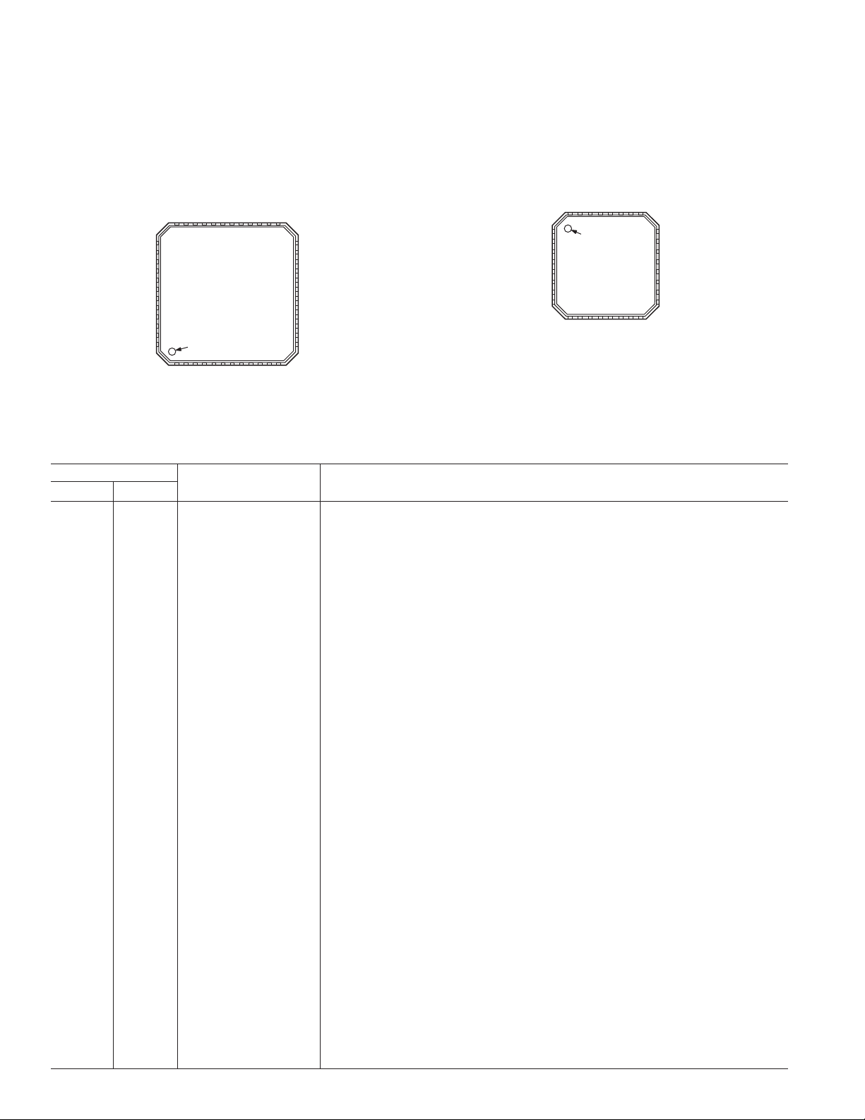
PIN CONFIGURATIONS
GND2 37
VCC2 38
IMODN 39
IMODN 40
GND2 41
IMODP 42
IMODP 43
GND2 44
GND2 45
IBIAS 46
IBIAS 47
CCBIAS 48
48-Lead LFCSP
36 GND2
35 IDTONE
34 GND2
33 IBMON
32 IMMON
31 GND3
30 VCC3
29 ALS
28 FAIL
27 DEGRADE
ADN2841
TOP VIEW
(Not to Scale)
PIN 1
INDICATOR
GND 1
PSET 5
ASET 3
ERSET 4
LBWSET 2
GND 6
IMPD 7
IMPDMON 8
IMPD2 10
IMPDMON2 9
26 CLKSEL
25 GND
24 GND
23 GND
22 CLKN
21 CLKP
20 GND1
19 DATAP
18 DATAN
17 GND1
16 VCC1
15 GND
14 PAVCAP
13 ERCAP
VCC4 12
GND4 11
LBWSET 1
ASET 2
ERSET 3
PSET 4
IMPD 5
IMPDMON 6
GND4 7
VCC4 8
32-Lead LFCSP
32 CCBIAS
31 IBIAS
30 GND2
29 GND2
28 IMODP
27 GND2
26 IMODN
25 VCC2
PIN 1
INDICATOR
ADN2841
TOP VIEW
(Not to Scale)
VCC1 11
CLKP 15
GND1 14
CLKN 16
DATAP 13
DATAN 12
ERCAP 9
PAV CAP 10
24 IBMON
23 IMMON
22 GND3
21 VCC3
20 ALS
19 FAIL
18 DEGRADE
17 CLKSEL
PIN FUNCTION DESCRIPTIONS
Pin No.
48-Lead 32-Lead Mnemonic Function
1 GND Supply Ground
21 LBWSET Select Low Loop Bandwidth (Active = VCC)
32 ASET Alarm Current Threshold Setting Pin
43 ERSET Extinction Ratio Set Pin
54 PSET Average Optical Power Set Pin
6 GND Ground
75 IMPD Monitor Photodiode Input
86 IMPDMON Mirrored Current from Monitor Photodiode
9 IMPDMON2 Mirrored Current from Monitor Photodiode 2 (for Use with Two MPDs)
10 IMPD2 Monitor Photodiode Input 2–(for Use with Two MPDs)
11 7 GND4 Supply Ground
12 8 VCC4 Supply Voltage
13 9 ERCAP Extinction Ratio Loop Capacitor
14 10 PAVCAP Average Power Loop Capacitor
15 GND Ground
16 11 VCC1 Supply Voltage
17 GND1 Supply Ground
18 12 DATAN Data, Negative Differential Terminal
19 13 DATAP Data, Positive Differential Terminal
20 14 GND1 Supply Ground
21 15 CLKP Data Clock Positive Differential Terminal, used if CLKSEL = V
22 16 CLKN Data Clock Negative Differential Terminal, used if CLKSEL = V
CC
CC
23 GND Ground
24 GND Ground
25 GND Ground
26 17 CLKSEL Clock Select (Active = V
), used if data is clocked into chip
CC
27 18 DEGRADE DEGRADE Alarm Output
28 19 FAIL FAIL Alarm Output
29 20 ALS Automatic Laser Shutdown
30 21 VCC3 Supply Voltage
31 22 GND3 Supply Ground
32 23 IMMON Modulation Current Mirror Output
33 24 IBMON Bias Current Mirror Output
34 GND2 Supply Ground
35 IDTONE IDTONE (Requires External Current Sink to Ground)
36 GND2 Supply Ground
–4–
REV. A

ADN2841
PIN FUNCTION DESCRIPTIONS (continued)
Pin No.
48-Lead 32-Lead Mnemonic Function
37 GND2 Supply Ground
38 25 VCC2 Supply Voltage
39 26 IMODN Modulation Current Negative Output. Connect to 25 Ω.
40 IMODN Modulation Current Negative Output. Connect to 25 Ω.
41 27 GND2 Supply Ground
42 28 IMODP Modulation Current Positive Output. Connect to laser diode.
43 IMODP Modulation Current Positive Output. Connect to laser diode.
44 29 GND2 Supply Ground
45 30 GND2 Supply Ground
46 31 IBIAS Laser Diode Bias Current
47 IBIAS Laser Diode Bias Current
48 32 CCBIAS Extra Laser Diode Bias when AC-Coupled
REV. A
–5–

ADN2841
GENERAL
Laser diodes have current-in to light-out transfer functions as shown
in Figure 2. Two key characteristics of this transfer function are the
threshold current, I
, and the slope in the linear region beyond
TH
the threshold current, referred to as slope efficiency, LI.
P1
ER =
P0
P1 + P0
P
=
AV
2
P
P
LI =
I
I
TH
I
CURRENT
P
OPTICAL POWER
P1
AV
P0
Figure 2. Laser Transfer Function
CONTROL
A monitor photodiode (MPD) is required to control the LD. The
MPD current is fed into the ADN2841 to control the optical
power and extinction ratio, continuously adjusting the bias current
and modulation current in response to the laser’s changing
threshold current and light-to-current (LI) slope (slope efficiency).
The ADN2841 uses automatic power control (APC) to maintain a constant power over time and temperature.
The ADN2841 uses closed-loop extinction ratio control to allow
optimum setting of extinction ratio for every device. Therefore,
SONET/SDH interface standards can be met over device variation, temperature, and time. Closed-loop modulation control
eliminates the need to either overmodulate the LD or include
external components for temperature compensation. This reduces
research and development time and second-sourcing issues
caused by characterizing LDs.
Average power and extinction ratio are set using the PSET and
ERSET pins, respectively. Potentiometers are connected between
these pins and ground. The potentiometer R
change the average power. The potentiometer R
is used to
PSET
ERSET
is used
to adjust the extinction ratio. Both PSET and ERSET are
kept 1.23 V above GND.
R
and R
PSET
where I
AV
can be calculated using the following formulas:
ERSET
V
PSET
123.
=
I
AV
R
is the average MPD current.
V
R
ERSET
=
I
MPD CW
P
CW
123
ER
−
ER
1
××
02..
+
1
P
AV
–
×
where PCW is the dc optical power specified on the laser data
sheet, I
P
is the required average power.
AV
Note that I
is the MPD current at that specified PCW, and
MPD_CW
ERSET
and I
will change from device to device.
PSET
However, the control loops will determine actual values. It is not
required to know the exact values for LI or MPD optical coupling.
LOOP BANDWIDTH SELECTION
For anyrate operation, the user should hardwire the LBWSET
pin high and use 1 µF capacitors to set the actual loop band-
width. These capacitors are placed between the PAVCAP and
ERCAP pins and ground. It is important that these capacitors
be low leakage multilayer ceramics with an insulation resistance
greater than 100 GΩ or a time constant of 1000 sec, whichever
is less. The ADN2841 may be optimized for 2.7 Gbps operation
by keeping the LBWSET pin low. This results in a much shorter
loop time constant (a 10⫻ reduction). The value of PAVCAP
and ERCAP capacitors required for 2.5 Gbps operation is 22 nF.
ALARMS
The ADN2841 alarms are designed to allow interface complia nce
to ITU-T-G958 (11/94) section 10.3.1.1.2 (transmitter fail) and
section 10.3.1.1.3 (transmitter degrade). The ADN2841 has
two active high alarms, DEGRADE and FAIL. A resistor between
ground and the ASET pin is used to set the current at which
these alarms are raised. The current through the ASET resistor is
a ratio of 100:1 to the FAIL alarm threshold. The DEGRADE
alarm will be raised at 90% of this level.
Example:
ImAI mA
=∴ =50 45
FAIL DEGRADE
ImA
BIASTRIP
===µ
100
123 123
..
== =
I
ASET
I
ASET
R
ASET
NOTE: The smallest value for R
sponds to the I
maximum of 100 mA.
BIAS
50
100
V
V
A
500
is 1.2 kΩ, as this corre-
ASET
500
246
.µΩ
A
k
The laser degrade alarm, DEGRADE, gives a warning of imminent
laser failure if the laser diode degrades further or environmental
conditions, e.g., increasing temperature, continue to stress the LD.
The laser fail alarm, FAIL, is activated when the transmitter can
no longer be guaranteed to be SONET/SDH compliant. This
occurs when one of the following conditions arises:
•
The ASET threshold is reached.
•
The ALS pin is set high. This shuts off the modulation and
bias currents to the LD, resulting in the MPD current
dropping to zero. This gives closed-loop feedback to the
system in which ALS has been enabled.
DEGRADE will only be raised when the bias current exceeds
90% of ASET current.
MONITOR CURRENTS
IBMON, IMMON, IMPDMON, and IMPDMON2 are
cur
rent controlled current sources from VCC. They mirror the
bias, modulation, and MPD current for increased monitoring
functionality. An external resistor to GND gives a voltage
proportional to the current monitored.
DUAL MPD DWDM FUNCTION (48-LEAD LFCSP ONLY)
The ADN2841 has circuitry for an optional second monitor
photodiode, MPD2.
–6–
REV. A

REF CLOCK
20MHz–
180MHz
ADN2841
CLKIN
AD9850/AD9851
DDS
R
SET
CONTROLLER
1.25mA–20mA
I
OUT
I
OUT
50
37.5A–600A
50
LP FILTER
(DC-COUPLED)
BC550
1300
Figure 3. Circuitry to Allow Fiber Identification
The second photodiode current is mirrored to IMPDMON2
for wavelength control purposes and is summed internally for
the power control loop. For single MPD circuits, the MPD2 pin
is tied to GND.
This enables the system designer to use the two currents to
control the wavelength of the laser diode using various optical
filtering techniques inside the laser module.
If the monitor current functions, IMPDMON and IMPDMON2
are not required, the IMPD and IMPD2 pins can be grounded,
and the monitor photodiode output can be connected directly
to PSET.
IDTONE (48-LEAD LFCSP ONLY)
The IDTONE pin is supplied for fiber identification/supervisory
channels or control purposes in WDM. This pin modulates the
optical one level over a possible range of 2% of minimum IMOD
to 10% of maximum IMOD. The level of modulation is set by
connecting an external current sink between the IDTONE pin and
ground. There is a gain of two from this pin to the IMOD current.
Figure 3 shows how an AD9850/AD9851 DDS may be used
with the ADN2841 to allow fiber identification.
Note that using IDTONE during transmission may cause optical eye degradation.
DATA, CLOCK INPUTS
Data and clock inputs are ac-coupled (10 nF recommended)
and terminated via a 100 Ω internal resistor between DATAP
and DATAN and also between CLKP and CLKN pins. There
is a high impedance circuit to set the common-mode voltage
that is designed to change overtemperature. It is recommended
that ac-coupling be used to eliminate the need for matching
between common-mode voltages.
AD8602
1/2
10kHz–1MHz
0.125mA–2mA
BC550
IDTONE
ADN2841
500
AD8602
1/2
50A–800A
IMMON
1000
ADN2841
DATAP
DATAN
TO FLIP-FLOPS
50 50
V
REG
R
R = 2.5k, DATA
R = 3k, CLK
400A TYP
Figure 4. AC-Coupling of Data Inputs
CCBIAS
CCBIAS should be connected to the BIAS pin if the laser diode is
connected to the ADN2841 using a capacitor. CCBIAS is a
current sink to GND.
AUTOMATIC LASER SHUTDOWN
The ADN2841 ALS allows compliance to ITU-T-G958
(11/94), section 9.7.
When ALS is logic high, both bias and modulation currents are
turned off.
Correct operation of ALS can be confirmed by the fail alarm
being raised when ALS is asserted. Note this is the only time
that DEGRADE will be low while FAIL is high.
REV. A
–7–

ADN2841
ALARM INTERFACES
A 30 kΩ internal pull-up resistor is employed to pull the digital
high value of the alarm outputs to V
has a feature that allows the user to externally wire resistors in
parallel with the 30 kΩ pull-up resistors, thus enabling the user
to interface to non-V
be below the V
used for the ADN2841.
CC
levels. Non-VCC alarm output levels must
CC
POWER CONSUMPTION
The ADN2841 die temperature must be kept below 125°C.
The θ
is 25°C/W for the 48-lead LFCSP and 32°C/W for the
JA
32-lead LPCSP when soldered in a four-layered board. Both
LFCSP packages have an exposed paddle and as such need to
be soldered to the PCB to achieve this thermal performance.
TT P
=+×
DIE AMBIENT A
II I
=+03.
CC CCMIN MOD
PV I I V I V
=×+ ×
CC CC BIAS BIAS PIN MOD MOD PIN
()
Thus the maximum combination of I
calculated.
. However, the ADN2841
CC
θ
J
+×
__
()
BIAS
+ I
MOD
must be
V
CC
V
V
CC
IMPD
CC
ADN2841
IMODP
IBIAS
DATAP
DATAN
IDTONE
TX
RX
CLK
CS
ADN2850
SDI
SDO
CLK
CS
DAC1
DAC2
DATAP
DATAN
IDTONE
PSET
ERSET
Figure 5. Application Using Optical Supervisor ADN2850
as a Dual 10-Bit Digital Potentiometer Using Thin-Film
Resistor Technology to Give Very Low Temperature
Coefficients
FU-445SDF-WM1
V
CC
V
CC
V
CC
V
CC
25
V
CC
CCBIAS
V
CC
GND2
36 25
37
GND2
VCC2 GND
IMODN CLKN
IMODN CLKP
GND2 GND1
IMODP DATAP
IMODP DATAN
GND2 GND1
GND2 VCC1
IBIAS GND
IBIAS PAVCAP
48
1
GND
GND2
IDTONE
ASET
LBWSET
IBMON
ADN2841
ERSET
GND3
IMMON
GND
PSET
ALS
VCC3
IMPDMON
IMPD
1.5k
GND
FAIL
CLKSEL
DEGRADE
ERCAP
IMPD2
IMPDMON2
VCC4
GND4
GND
13
24
GND
12
V
CC
FAIL
DEGRADE
CLKN
CLKP
DATAP
DATAN
V
s SHOULD HAVE BYPASS CAPACITORS AS CLOSE AS POSSIBLE TO THE
CC
ACTUAL SUPPLY PINS ON THE ADN2841 AND THE LASER DIODE USED.
100nF 100nF 100nF 100nF 10F
GND
Figure 6. 2.7 Gbps Test Circuit, DC-Coupled, Data Not Clocked, Fast Loop Time Constant Selected
–8–
REV. A

ADN2841
V
CC
V
CC
V
CC
25
V
CC
V
CC
V
V
CC
CC
CCBIAS
GND2
36
37
GND2
VCC2 GND
IMODN CLKN
IMODN CLKP
GND2 GND1
IMODP DATAP
IMODP DATAN
GND2 GND1
GND2 VCC1
IBIAS GND
IBIAS PAVCAP
48
1
GND
V
CC
IDTONE
GND2
ASET
LBWSET
IBMON
ADN2841
ERSET
GND3
IMMON
GND
PSET
ALS
VCC3
IMPDMON
IMPD
1.5k
FAIL
CLKSEL
DEGRADE
ERCAP
IMPD2
IMPDMON2
GND4
25
GND
GND
13
VCC4
24
12
GND
V
CC
FAIL
DEGRADE
CLKN
CLKP
DATAP
DATAN
VCCs SHOULD HAVE BYPASS CAPACITORS AS CLOSE AS POSSIBLE TO THE
ACTUAL SUPPLY PINS ON THE ADN2841 AND THE LASER DIODE USED.
100nF 100nF 100nF 100nF 10F
GND
Figure 7. Anyrate Test Circuit, Capacitively Coupled, Data Clocked, Slow Loop Time Constant Selected
REV. A
–9–

ADN2841
V
V
CC
V
CC
CC
GND4
EA MODULATOR
V
1
V
CC
VCC4
12
CC
48
CCBIAS
GND
LBWSET
ASET
ERSET
PSET
GND
IMPD
IMPDMON
IMPDMON2
IMPD2
100nH
IBIAS
PAV CAP
ERCAP
10nF
IBIAS
GND2
ADN2841
VCC1
GND
V
CC
GND2
GND1
75
IMODP
IMODP
DATAP
DATAN
GND2
IMODN
CLKP
GND1
1
1/2 OP293
33
V
CC
VCC2
GND2
IMODN
IDTONE
GND2
IBMON
IMMON
GND3
VCC3
ALS
FAIL
DEGRADE
CLKSEL
GND
CLKN
GND
V
CC
V
CC
8
2
3
NOTES
1. V
s SHOULD HAVE BYPASS CAPACITORS
CC
AS CLOSE AS POSSIBLE TO THE ACTUAL
SUPPLY PINS ON THE ADN2841 AND THE
LASER DIODE USED.
2. THE OP293 HAS BEEN SELECTED BECAUSE
OF ITS GAIN-BANDWIDTH PRODUCT AND
SHOULD BE USED IN THIS APPLICATION.
36
GND2
V
CC
V
CC
V
24
CC
DAC
1k
Figure 8. Applications Circuit
Figure 9. Unfiltered 2.5 Gbps Optical Eye. Average
Power = –3 dBm, Extinction Ratio = 9.5 dB. Eye
Obtained Using a Mitsubishi FU-445-SDF.
1/2 OP293 6
7
–V
CC
5
DAC
1k
Figure 10. Filtered 2.5 Gbps Optical Eye. Average
Power = –3 dBm, Extinction Ratio = 9 dB. Eye
Obtained Using a Mitsubishi FU-445-SDF.
–10–
REV. A

OUTLINE DIMENSIONS
48-Lead Frame Chip Scale Package [LFCSP]
(CP-48)
Dimensions shown in millimeters
ADN2841
1.00
0.90
0.80
0.25
REF
12 MAX
SEATING
PLANE
BSC SQ
PIN 1
INDICATOR
VIEW
7.00
0.60 MAX
TOP
0.70 MAX
0.65 NOM
0.50 BSC
COMPLIANT TO JEDEC STANDARDS MO-220-VKKD-2
6.75
BSC SQ
0.50
0.40
0.30
0.05 MAX
0.02 NOM
COPLANARITY
0.08
37
36
25
24
0.60 MAX
BOTTOM
VIEW
5.50
REF
0.30
0.23
0.18
PIN 1
INDICATOR
48
1
5.25
4.70
2.25
12
13
PIN 1
INDICATOR
1.00
0.90
0.80
32-Lead Frame Chip Scale Package [LFCSP]
(CP-32)
Dimensions shown in millimeters
5.00
12 MAX
SEATING
PLANE
BSC SQ
0.30
0.23
0.18
4.75
BSC SQ
0.25 REF
TOP
VIEW
0.70 MAX
0.65 NOM
COMPLIANT TO JEDEC STANDARDS MO-220-VHHD-2
0.05 MAX
0.02 NOM
COPLANARITY
0.60 MAX
0.50
BSC
0.50
0.40
0.30
0.08
24
17
0.60 MAX
25
16
BOTTOM
VIEW
3.50
REF
PIN 1
32
9
INDICATOR
1
3.25
SQ
3.10
2.95
8
REV. A
–11–

Revision History
Location Page
8/02—Data Sheet changed from REV. 0 to REV. A.
Figure 8 replaced . . . . . . . . . . . . . . . . . . . . . . . . . . . . . . . . . . . . . . . . . . . . . . . . . . . . . . . . . . . . . . . . . . . . . . . . . . . . . . . . . . . . . . . 10
Updated Outlines . . . . . . . . . . . . . . . . . . . . . . . . . . . . . . . . . . . . . . . . . . . . . . . . . . . . . . . . . . . . . . . . . . . . . . . . . . . . . . . . . . . . . . 11
C02659–0–9/02(A)
–12–
PRINTED IN U.S.A.
REV. A
 Loading...