10.7 Gbps, 3.3 V, Low Noise,
FEATURES
Technology: high performance SiGe
Bandwidth: 9 GHz
Input noise current density: 1.0 µA
Optical sensitivity: –19.3 dBm
Differential transimpedance: 5000 V/A
Power dissipation: 200 mW
Input current overload: 2.8 mA p-p
Linear input range: 0.15 mA p-p
Output resistance: 50 Ω/side
Output offset adjustment range: 240 mV
Average input power monitor: 1 V/mA
Die size: 0.87 mm × 1.06 mm
APPLICATIONS
10.7 Gbps optical modules
SONET/SDH OC-192/STM-64 and 10 GbE
receivers, transceivers, and transponders
3.3V
R
F
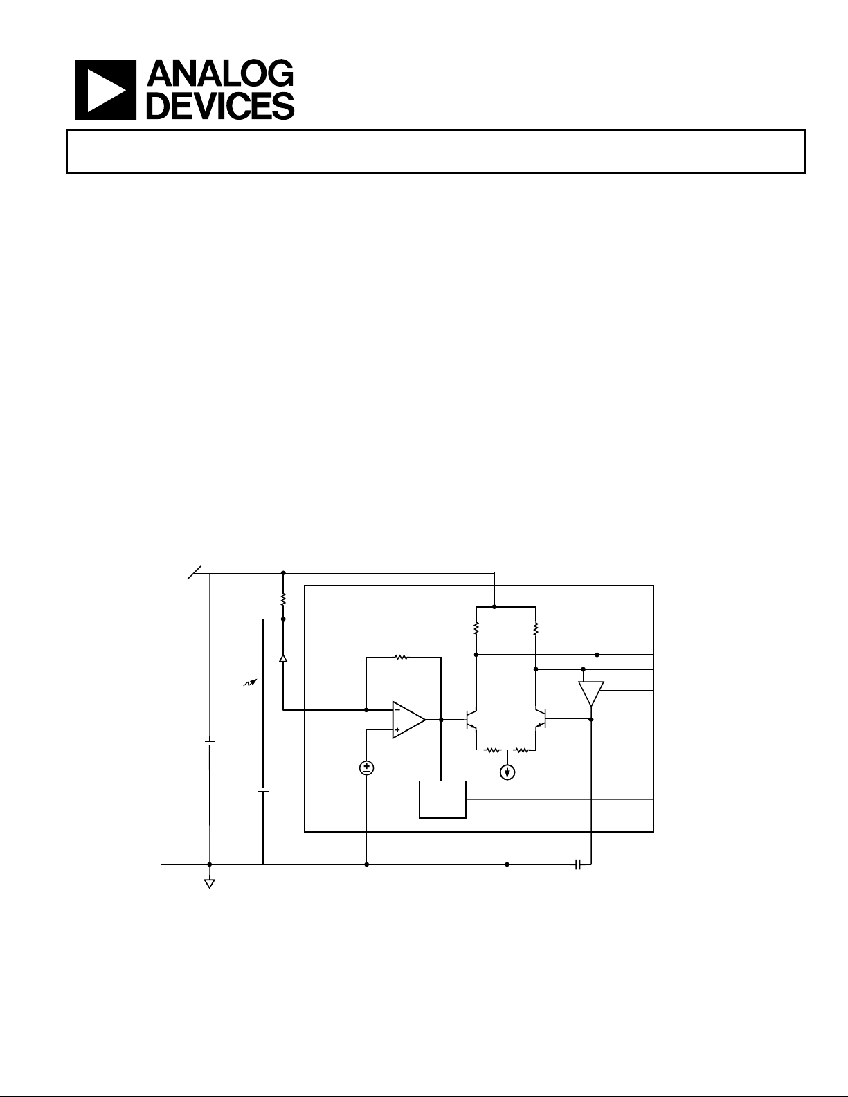
TIA with Average Power Monitor
FUNCTIONAL BLOCK DIAGRAM
ADN2820
PRODUCT DESCRIPTION
The ADN2820 is a compact, high performance, 3.3 V power
supply SiGe transimpedance amplifier (TIA) optimized for
10 Gbps Metro-Access and Ethernet systems. It is a single chip
solution for detecting photodiode current with a differential
output voltage. The ADN2820 features low input referred noise
current and high output transimpedance gain, capable of
driving a typical CDR or transceiver directly. A POWMON
output is provided for input average power monitoring and
alarm generation. Low nominal output offset enables dc output
coupling to 3.3 V circuits. The OFFSET control input enables
output slice level adjustment for asymmetric input signals. The
ADN2820 operates with a 3.3 V power supply and is available in
die form.
VCC (1,2,3)
RF = 500Ω
hυ
IN (13)'
C
B
0.85V
C
F
GND (10, 11)
Figure 1. Functional Block Diagram/Typical Operating Circuit
Rev. 0
Information furnished by Analog Devices is believed to be accurate and reliable.
However, no responsibility is assumed by Analog Devices for its use, nor for any
infringements of patents or other rights of third parties that may result from its use.
Specifications subject to change without notice. No license is granted by implication
or otherwise under any patent or patent rights of Analog Devices. Trademarks and
registered trademarks are the property of their respective owners.
50Ω
One Technology Way, P.O. Box 9106, Norwood, MA 02062-9106, U.S.A.
Tel: 781.329.4700
Fax: 781.326.8703 © 2003 Analog Devices, Inc. All rights reserved.
A
V
50Ω
= 20dB
GND (4,7)
OUT (5)
OUTB (6)
OFFSET (14)
20mA
POWMON (8)
CLF (9)
CLF
www.analog.com
03194-0-001

ADN2820
TABLE OF CONTENTS
Specifications..................................................................................... 3
Absolute Maximum Ratings............................................................ 4
ESD Caution.................................................................................. 4
Pad Layout and Functional Descriptions ......................................5
Pad Layout..................................................................................... 5
Die Information............................................................................ 5
Pad Descriptions........................................................................... 5
Pad Coordinates ........................................................................... 5
Typical Performance Characteristics .............................................6
REVISION HISTORY
Revision 0: Initial Version
Applications........................................................................................8
Optical Sensitivity .........................................................................8
Optical Power Monitor.................................................................8
Output Offset Adjust Input..........................................................9
Low Frequency Transimpedance Cutoff Capacitor Selection.9
Bandwidth versus Input Bond Wire Inductance.................... 10
Bandwidth versus Output Bond Wire Inductance................. 10
Butterfly Package Assembly...................................................... 11
Outline Dimensions....................................................................... 12
Ordering Guide .......................................................................... 12
Rev. 0 | Page 2 of 12

ADN2820
SPECIFICATIONS
Table 1. Electrical Specifications
Parameter Conditions
DYNAMIC PERFORMANCE
Bandwidth
Total Input RMS Noise
1, 2
1, 2
–3 dB 7.5 9 GHz
DC to 10 GHz 1.0 µA
Small Signal Transimpedance 100 MHz 4000 5000 6000 V/A
Transimpedance Ripple2 100 MHz to 3 GHz ±0.5 dB
Group Delay Variation2 100 MHz to 3 GHz ±10 ps
100 MHz to 9 GHz ±30 ps
Total Peak-to-Peak Jitter
2, 3
I
IN,P-P
Low Frequency Cutoff CLF = 0.1 µF 12 kHz
S22 DC – 10 GHz, differential –10 dB
Linear Input Range Peak-to-peak, <1 dB compression 0.15 mA
Input Overload Current
1, 2
ER = 10 dB 1.4 2.8 mA p-p
ER = 4 dB 1.0 1.9 mA p-p
Maximum Output Swing Differential, I
DC PERFORMANCE
Power Dissipation 147 200 264 mW
Input Voltage 0.75 0.85 0.93 V
Output Common-Mode Voltage DC terminated to VCC VCC – 0.3 V
Output Offset I
IN, AVE
Offset Adjust Sensitivity See Figure 3 120 mV/V
Offset Adjust Range See Figure 3 240 mV
POWMON Sensitivity I
POWMON Offset I
IN, AVE
IN, AVE
1
Min/Max VCC = 3.3 V ± 0.3 V, T
2
Photodiode capacitance CD = 0.22 pF ± 0.04 pF; photodiode resistance = 20 Ω; CB = CF = 100 pF; RF = 100 Ω; input wire bond inductance LIN = 0.5 nH ± 0.15 nH; output
bond wire inductance L
–12
3
10
BER, 8 dB extinction ratio, 0.85 A/W PIN responsivity.
OUT, OUTB
= –15°C to +85°C; Typ VCC = 3.3 V, T
AMBIENT
= 0.85 nH ± 0.15 nH; load impedance = 50 Ω (each output, dc- or ac-coupled).
1
Min Typ Max Unit
= 2.5 mA 17 ps
= 2.0 mA 0.88 1.1 V p-p
IN P-P
< 0.1 mA –20 ±3 +20 mV
= 10 µA to 1 mA 0.76 1 1.2 V/mA
= 0 µA 20 mV
= 25°C.
AMBIENT
Rev. 0 | Page 3 of 12

ADN2820
ABSOLUTE MAXIMUM RATINGS
Table 2. ADN2820 Absolute Maximum Ratings
Parameter Rating
Supply Voltage (VCC to GND) 5.2 V
Internal Power Dissipation
Output Short Circuit Duration Indefinite
Maximum Input Current 5 mA
Storage Temperature Range –65°C to +125°C
Operating Ambient Temperature Range –15°C to +85°C
Maximum Junction Temperature 165°C
Die Attach Temperature (<60 seconds) 450°C
ESD CAUTION
ESD (electrostatic discharge) sensitive device. Electrostatic charges as high as 4000 V readily
accumulate on the human body and test equipment and can discharge without detection. Although
this product features proprietary ESD protection circuitry, permanent damage may occur on devices
subjected to high energy electrostatic discharges. Therefore, proper ESD precautions are
recommended to avoid performance degradation or loss of functionality.
Stresses above those listed under Absolute Maximum Ratings
may cause permanent damage to the device. This is a stress
rating only; functional operation of the device at these or any
other conditions above those indicated in the operational
section of this specification is not implied. Exposure to absolute
maximum rating conditions for extended periods may affect
device reliability.
Rev. 0 | Page 4 of 12
 Loading...