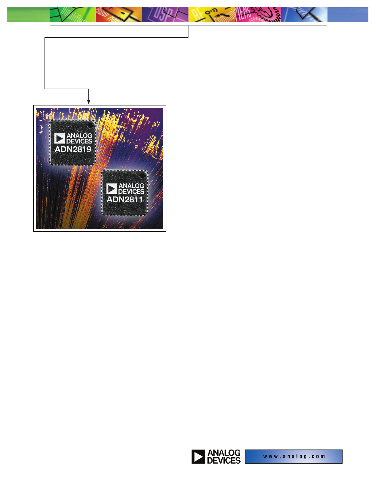
ADN2819/ADN2811—Multirate Limiting
Amplifi er and Clock and Data Recovery ICs
The proprietary delay and phase-locked loop design of the ADN2819
and ADN2811 provide unprecedented jitter performance for robust
high-speed networking designs.
Integrated Limiting Amplifi er with Adjustable Slice Level
Facilitates Design of High-Performance Fiber Optic Receivers
As the demand for bandwidth grows, Analog Devices continues to provide innovative solutions for fiber optic interface ICs that translate into
compelling competitive advantages for our customers.
Both the ADN2819 and the ADN2811 are user-friendly and flexible.
Native and forward error correction (FEC) digital “wrappers” are
supported for all rates without any change of reference clock.
An internal or external reference clock (at one of four frequencies) can
be used, and a multiplexer is incorporated to allow bypass of the CDR.
All of these features reduce time to market, minimize costs, and improve
manufacturability.
Analog has more than 10 years of experience designing fiber optic
components. Put our expertise to work for you.
Features
ADN2819/ADN2811
• Integrated limiting amplifier with adjustable slice
• Quantizer sensitivity: 6 mV
• Adjustable slice level: ±100 mV
• Exceeds all SONET/SDH requirements for jitter
transfer, generation, and tolerance
• Internal MUX to bypass CDR
• Low power: 550 mW typical
• One supply: 3.3 V ⫾10%
• Single reference clock frequency for all rates
• Loss-of-lock indicator
• Small footprint: 48-lead LFCSP package
(7 mm ⫻ 7 mm overall)
A prime example of Analog’s system knowledge and design expertise
working together are the ADN2819 and ADN2811. These highly integrated, low-power devices provide adjustable slice level quantization and
clock and data recovery functions with the ADN2819 supporting multirate operation up to 2.7 Gbps, and the ADN2811 supporting 2.5/2.7 Gbps
data rates only. Diagnostic capabilities include a signal detector with
user-adjustable threshold and 3 dB optical hysteresis to prevent chatter, a
loss-of-lock detector, and loop-back mode.
The proprietary delay and phase-locked loop architecture of
the ADN2819 and ADN2811 ensure that every SONET/SDH
jitter requirement is exceeded over all operating conditions.
Low bandwidth jitter transfer simultaneous with high bandwidth jitter
tolerance and minimal jitter peaking create an ideal scenario in
regenerator applications.
ADN2819
• Multirate (155/166 Mbps, 622/666 Mbps,
1.25/1.34 Gbps, 2.49/2.67 Gbps)
ADN2811
• Dual rate 2.5/2.7 Gbps
Applications
• SONET OC–3/12/48, SDH STM–1/4/16, Gb Ethernet, and all
associated FEC rates
• WDM transponders
• SONET/SDH regenerators
• SONET/SDH test equipment
• Backplane applications

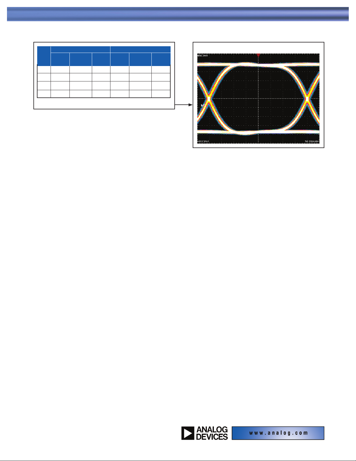
Typical Jitter Transfer Typical Jitter Tolerance
SONET ADN2819/ SONET ADN2819/
Rate Spec ADN2811 Margin Spec ADN2811 Margin
OC48 2 MHz 666 kHz 3.0 1 MHz 4.8 MHz 4.8
GbE (1 MHz) 333 kHz 3.0
(500 kHz)
4.8 MHz 9.6
OC12 500 kHz 167 kHz 3.0 250 kHz 4.8 MHz 19.2
OC3 130 kHz 41 kHz 3.2 65 kHz 0.6 MHz 9.2
Exceeds all SONET/SDH jitter requirements for exceptional performance
PRBS23 PATTERN
TYPICAL OC–48 EYE DIAGRAM
This information applies to a product under development. Its characteristics and specifi cations
are subject to change without notice. Analog Devices assumes no obligation regarding future
manufacture, unless otherwise agreed to in writing. No responsibility is assumed by Analog
Devices for its use; nor for any infringement of patents or other rights of third parties that may
result from its use. No license is granted by implication or otherwise under any patent or patent
rights of Analog Devices.
Worldwide
Headquarters
One Technology Way
P.O. Box 9106
Norwood, MA
02062-9106 U.S.A.
Tel: 781 329 4700
(1 800 262 5643,
U.S.A. Only)
Fax: 781 326 8703
© Analog Devices, Inc., 2002. All rights reserved. Trademarks and
registered trademarks are the property of their respective companies.
Printed in the U.S.A. H02888-1-3/02(0)
Analog Devices
GmbH
Am Westpark 1–3
D-81373
München, Germany
Tel: 49 89 76903 0
Fax: 49 89 76903 157
Japan
Headquarters
New Pier Takeshiba
South Tower Building
1-16-1 Kaigan,
Minato-ku
Tokyo 105-6891,
Japan
Tel: 3 5402 8200
Fax: 3 5402 1063
Southeast Asia
Headquarters
4501 Nat West Tower
Times Square
1 Matheson Street
Causeway Bay,
Hong Kong, PRC
Tel: 852 2 506 9336
Fax: 852 2 506 4755
 Loading...