

Continuous Rate 10 Mbps to 2.7 Gbps Clock
www.BDTIC.com/ADI
FEATURES
Serial data input: 10 Mbps to 2.7 Gbps
Exceeds ITU-T jitter specifications
Integrated limiting amplifier
5 mV sensitivity (ADN2817 only)
Adjustable slice level: ±100 mV (ADN2817 only)
Patented dual-loop clock recovery architecture
Programmable LOS detect (ADN2817 only)
Integrated PRBS generator and detector
No reference clock required
Loss of lock indicator
Supports double data rate
Bit error rate monitor (BERMON) or sample phase adjust options
Rate selectivity without the use of a reference clock
2
I
C interface to access optional features
Single-supply operation: 3.3 V
Low power
650 mW (ADN2817)
600 mW (ADN2818)
5 mm × 5 mm 32-lead LFCSP
APPLICATIONS
SONET OC-1, OC-3, OC-12, OC-48, and all associated FEC rates
Fibre Channel, 2× Fibre Channel, GbE, HDTV, and others
WDM transponders
Regenerators/repeaters
Test equipment
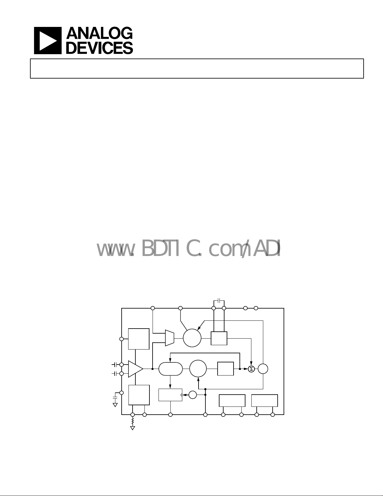
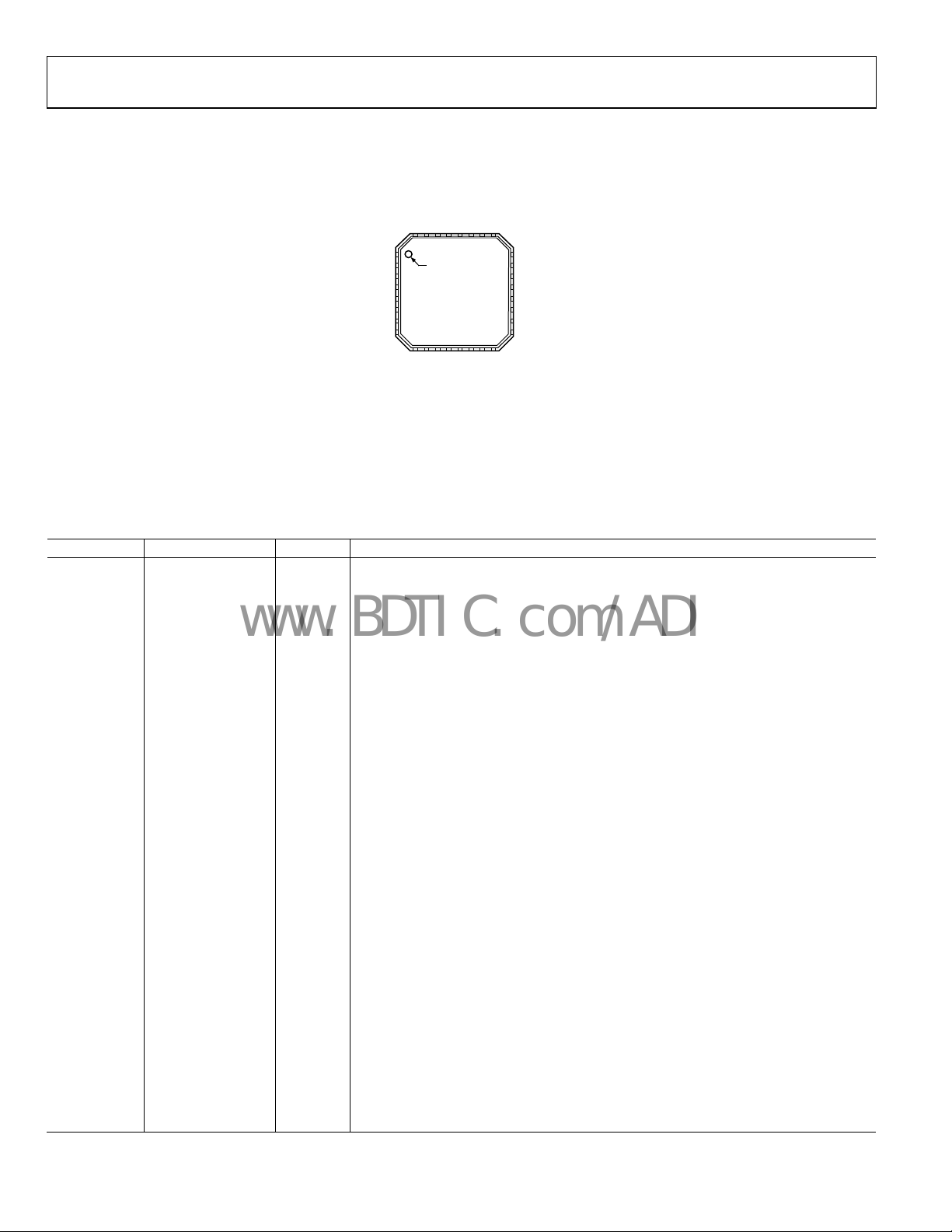
FUNCTIONAL BLOCK DIAGRAM
REFCLKP/REFCLKN
(OPTIO NAL)
LOL
and Data Recovery ICs
ADN2817/ADN2818
GENERAL DESCRIPTION
The ADN2817/ADN2818 provide the receiver functions of
quantization, signal level detect, and clock and data recovery for
continuous data rates from 10 Mbps to 2.7 Gbps. The ADN2817/
ADN2818 automatically lock to all data rates without the need for
an external reference clock or programming. All SONET jitter
requirements are exceeded, including jitter transfer, jitter generation,
and jitter tolerance. All specifications are quoted for −40°C to
+85°C ambient temperature, unless otherwise noted.
This device, together with a PIN diode and a TIA preamplifier,
can implement a highly integrated, low cost, and low power
fiber optic receiver.
The ADN2817/ADN2818 have many optional features available
through an I
the data rate onto which the ADN2817 or ADN2818 is locked,
or the user can set the device to lock only to one particular data
rate if provisioning of data rates is required. A BERMON circuit
provides an estimate of the received bit error rate (BER) without
interruption of the data. Alternatively, the user can adjust the
data sampling phase to optimize the received BER.
The ADN2817/ADN2818 are available in a compact 5 mm ×
5 mm, 32-lead, lead frame chip scale package.
CF1 CF2
2
C® interface. For example, the user can read back
VCC VEE
SLICE
THRADJ
ADJUST
(ADN2817
ONLY)
LOS
DETECT
(ADN2817
ONLY)
LOS DATAOUTP/
PHASE
SHIFTER
DATA
RETIMING
DATAOUTN
SLICEP/
SLICEN
PIN
NIN
VREF
Rev. A
Information furnished by Analog Devices is believed to be accurate and reliable. However, no
responsibility is assumed by Analog Devices for its use, nor for any infringements of patents or other
rights of third parties that may result from its use. Specifications subject to change without notice. No
license is granted by implication or otherwise under any patent or patent rights of Analog Devices.
Trademarks and registered trademarks are the property of their respective owners.
FREQ/
LOCK
DET
PHASE
DET
ΔФ
CLKOUTP/
CLKOUTN
Figure 1.
ADN2817/ADN2818
LOOP
FILTER
LOOP
FILTER
BERMON
VBER BERMODE
One Technology Way, P.O. Box 9106, Norwood, MA 02062-9106, U.S.A.
Tel: 781.329.4700 www.analog.com
Fax: 781.461.3113 ©2007–2008 Analog Devices, Inc. All rights reserved.
VCO
I2C
REGISTERS
SCK SDA
06001-001

ADN2817/ADN2818
www.BDTIC.com/ADI
TABLE OF CONTENTS
Features .............................................................................................. 1
Applications ....................................................................................... 1
General Description ......................................................................... 1
Functional Block Diagram .............................................................. 1
Revision History ............................................................................... 2
Specifications ..................................................................................... 3
Jitter Specifications ....................................................................... 4
Output and Timing Specifications ............................................. 5
Bit Error Rate Monitor Specifications ....................................... 7
Timing Characteristics ................................................................ 8
Absolute Maximum Ratings ............................................................ 9
Thermal Characteristics .............................................................. 9
ESD Caution .................................................................................. 9
Pin Configuration and Function Descriptions ........................... 10
Typical Performance Characteristics ........................................... 11
I2C Interface Timing and Internal Register Description ........... 13
Terminology .................................................................................... 17
Input Sensitivity and Input Overdrive ..................................... 17
Single-Ended vs. Differential .................................................... 17
LOS Response Time ................................................................... 17
Jitter Specifications ......................................................................... 18
Jitter Generation ......................................................................... 18
Jitter Transfer ............................................................................... 18
Jitter Tolerance ............................................................................ 18
Theory of Operation ...................................................................... 19
Functional Description .................................................................. 21
Frequency Acquisition ............................................................... 21
Lock Detector Operation .......................................................... 21
Harmonic Detector .................................................................... 22
Limiting Amplifier (ADN2817 Only) ..................................... 22
Slice Level Adjust (ADN2817 Only) ........................................ 22
Loss of Signal (LOS) Detector (ADN2817 Only) .................. 22
Sample Phase Adjust .................................................................. 23
Bit Error Rate (BER) Monitor ................................................... 23
Squelch Mode ............................................................................. 24
I2C Interface ................................................................................ 24
Reference Clock (Optional) ...................................................... 25
Additional Features Available via the I2C Interface ............... 27
Applications Information .............................................................. 29
PCB Design Guidelines ............................................................. 29
DC-Coupled Application .......................................................... 31
Coarse Data Rate Readback Look-Up Table ............................... 32
HI_CODE and LO_CODE Look-Up Table ................................ 34
Outline Dimensions ....................................................................... 37
Ordering Guide .......................................................................... 37
REVISION HISTORY
8/08—Rev. 0 to Rev. A
Changes to Features Section, General Description Section, and
Figure 1 .............................................................................................. 1
Added Bit Rate Monitor Specifications Section and Table 4;
Renumbered Sequentially ................................................................ 7
Changes to Figure 5 and Table 6 ................................................... 10
Changes to Table 7 and Table 8 ..................................................... 14
Changes to Table 14 ........................................................................ 15
Added Table 15 ............................................................................... 15
Added Table 16 ............................................................................... 16
Added Sample Phase Adjust Section and Bit Error Rate (BER)
Monitor Section .............................................................................. 23
Added Figure 32; Renumbered Sequentially .............................. 24
Changes to Figure 36 ...................................................................... 29
Added Exposed Pad Notation to Outline Dimensions ............. 37
7/07—Revision 0: Initial Version
Rev. A | Page 2 of 40
ADN2817/ADN2818
www.BDTIC.com/ADI
SPECIFICATIONS
TA = T
unless otherwise noted.
Table 1.
Parameter Conditions Min Typ Max Unit
QUANTIZER—DC CHARACTERISTICS
QUANTIZER—AC CHARACTERISTICS
QUANTIZER—SLICE ADJUSTMENT ADN2817 only
LOSS OF SIGNAL DETECT (LOS) ADN2817 only
R
R
R
LOSS OF LOCK DETECT (LOL)
ACQUISITION TIME
DATA RATE READBACK ACCURACY
MIN
to T
, VCC = V
MAX
MIN
to V
, VEE = 0 V, CF = 0.47 µF, SLICEP = SLICEN = VEE, input data pattern: PRBS 223 − 1,
MAX
Input Voltage Range @ PIN or NIN, dc-coupled 1.8 2.8 V
Peak-to-Peak Differential Input PIN − NIN 2.0 V
Input Common-Mode Level DC-coupled (see Figure 40, Figure 41, and Figure 42) 2.3 2.5 2.8 V
Differential Input Sensitivity 223 − 1 PRBS, ac-coupled,1 BER = 1 × 10
−10
ADN2817 10 5 mV p-p
ADN2818 200 mV p-p
Data Rate 10 2700 Mbps
S11 @ 2.5 GHz −15 dB
Input Resistance Differential 100 Ω
Input Capacitance 0.65 pF
Gain SLICEP − SLICEN = ±0.5 V 0.10 0.11 0.13 V/V
Differential Control Voltage Input SLICEP − SLICEN −0.95 +0.95 V
Control Voltage Range DC level @ SLICEP or SLICEN VEE 0.95 V
Slice Threshold Offset ±1 mV
Loss of Signal Detect Range (See Figure 6) R
= 0 Ω 14.2 20.0 mV
Thresh
= 100 kΩ 2.1 5.0 mV
Thresh
Hysteresis (Electrical)
OC-48 R
OC-1 R
LOS Assert Time DC-coupled
LOS Deassert Time DC-coupled
= 0 Ω 6.2 8.2 dB
Thresh
= 100 kΩ 4.7 7.7 dB
Thresh
= 0 Ω 4.9 7.5 dB
Thresh
= 10 kΩ 3.0 7.3 dB
Thresh
2
2
500 ns
450 ns
VCO Frequency Error for LOL Assert With respect to nominal 1000 ppm
VCO Frequency Error for LOL Deassert With respect to nominal 250 ppm
LOL Response Time
OC-48 1.0 μs
OC-12 1.0 μs
10 Mbps 500 μs
Lock to Data Mode
OC-48 1.3 ms
OC-12 2.0 ms
OC-3 3.4 ms
OC-1 9.8 ms
10 Mbps 40.0 ms
Optional Lock to REFCLK Mode 10.0 ms
Coarse Readback See Tab le 19 10 %
Fine Readback In addition to REFCLK accuracy 100 ppm
Rev. A | Page 3 of 40
ADN2817/ADN2818
www.BDTIC.com/ADI
Parameter Conditions Min Typ Max Unit
POWER SUPPLY
Voltage 3.0 3.3 3.6 V
Current
ADN2817 210 247 mA
ADN2818 180 217 mA
OPERATING TEMPERATURE RANGE −40 +85 °C
1
PIN and NIN should be differentially driven and ac-coupled for optimum sensitivity.
2
When ac-coupled, the LOS assert and deassert time is dominated by the RC time constant of the ac coupling capacitor and the 50 Ω input termination of the ADN2817
input stage.
JITTER SPECIFICATIONS
TA = T
unless otherwise noted.
Table 2.
Parameter Conditions Min Typ Max Unit
PHASE-LOCKED LOOP CHARACTERISTICS
1
Jitter tolerance of the ADN2817/ADN2818 at these jitter frequencies is better than what the test equipment is able to measure.
MIN
to T
, VCC = V
MAX
MIN
to V
, VEE = 0 V, CF = 0.47 F, SLICEP = SLICEN = VEE, input data pattern: PRBS 223 − 1,
MAX
Jitter Transfer Bandwidth
OC-48 548 839 kHz
OC-12 93 137 kHz
OC-3 30 40 kHz
Jitter Peaking
OC-48 0 0.03 dB
OC-12 0 0.03 dB
OC-3 0 0.03 dB
Jitter Generation
OC-48 12 kHz to 20 MHz 0.001 0.003 UI rms
0.02 0.046 UI p-p
OC-12 12 kHz to 5 MHz 0.001 0.004 UI rms
0.01 0.036 UI p-p
OC-3 12 kHz to 1.3 MHz 0.001 0.004 UI rms
0.01 0.023 UI p-p
Jitter Tolerance 223 − 1 PRBS
OC-48 600 Hz
6 kHz
1
1
20.0 UI p-p
92.0 UI p-p
100 kHz 7.0 UI p-p
1 MHz
1
1.00 UI p-p
20 MHz 0.53 UI p-p
OC-12 30 Hz
300 Hz
1
100.0 UI p-p
1
44.0 UI p-p
25 kHz 7.35 UI p-p
250 kHz
1
1.00 UI p-p
5 MHz 0.52 UI p-p
OC-3 30 Hz
300 Hz
1
50.0 UI p-p
1
23.5 UI p-p
6500 Hz 6.71 UI p-p
65 kHz
1
1.00 UI p-p
130 kHz 0.54 UI p-p
Rev. A | Page 4 of 40
ADN2817/ADN2818
www.BDTIC.com/ADI
OUTPUT AND TIMING SPECIFICATIONS
Table 3.
Parameter Conditions Min Typ Max Unit
CML OUPUT CHARACTERISTICS (CLKOUTP/CLKOUTN,
DATAOUTP/DATAOUTN)
Single-Ended Output Swing, VSE See Figure 3 300 350 600 mV
Differential Output Swing, V
See Figure 3 600 700 1200 mV
DIFF
Output Voltage
High, VOH VCC V
Low, VOL VCC − 0.6 VCC − 0.35 VCC − 0.3 V
CML Outputs Timing
Rise Time 20% to 80% 80 112 ps
Fall Time 80% to 20% 80 123 ps
Setup Time, tS See Figure 2, OC-48 150 200 250 ps
Hold Time, tH See Figure 2, OC-48 150 200 250 ps
Setup Time, t
Hold Time, t
See Figure 4, OC-48 140 170 200 ps
DDRS
See Figure 4, OC-48 200 230 260 ps
DDRH
I2C INTERFACE DC CHARACTERISTICS LVCMOS
Input Voltage
High, VIH 0.7 VCC V
Low, VIL 0.3 VCC V
Input Current VIN = 0.1 VCC or VIN = 0.9 VCC −10.0 +10.0 μA
Output Low Voltage VOL, IOL = 3.0 mA 0.4 V
I2C INTERFACE TIMING See Figure 22
SCK Clock Frequency 400 kHz
SCK Pulse Width High
High, t
Low, t
600 ns
HIGH
1300 ns
LOW
Start Condition
Hold Time, t
Setup Time, t
600 ns
HD;STA
600 ns
SU;STA
Data
Setup Time, t
Hold Time, t
100 ns
SU;DAT
300 ns
HD;DAT
SCK/SDA Rise/Fall Time, tR/tF 20 + 0.1 Cb 300 ns
Stop Condition Setup Time, t
Bus Free Time Between a Stop and a Start, t
600 ns
SU;STO
1300 ns
BUF
REFCLK CHARACTERISTICS Optional lock to REFCLK mode
Input Voltage Range @ REFCLKP or REFCLKN
VIL 0 V
VIH VCC V
Minimum Differential Input Drive 100 mV p-p
Reference Frequency 10 200 MHz
Required Accuracy 100 ppm
Rev. A | Page 5 of 40
ADN2817/ADN2818
www.BDTIC.com/ADI
Parameter Conditions Min Typ Max Unit
LVTTL DC INPUT CHARACTERISTICS
Input Voltage
High, VIH 2.0 V
Low, VIL 0.8 V
Input Current
High IIH, VIN = 2.4 V +5 μA
Low IIL, VIN = 0.4 V −5 μA
LVTTL DC OUTPUT CHARACTERISTICS
Output Voltage
High VOH, IOH = −2.0 mA 2.4 V
Low VOL, IOL = +2.0 mA 0.4 V
Rev. A | Page 6 of 40
ADN2817/ADN2818
www.BDTIC.com/ADI
BIT ERROR RATE MONITOR SPECIFICATIONS
TA = T
unless otherwise noted.
Table 4.
Parameter Conditions Min Typ Max Unit
BERMON Extrapolation Mode I2C controlled eye profiling
BERMON Voltage Output Mode Analog voltage output
Sample Phase Adjust Mode
to T
MIN
Final Computed BER Accuracy
, VCC = V
MAX
MIN
to V
, VEE = 0 V, CF = 0.47 µF, SLICEP = SLICEN = VEE, input data pattern: PRBS 223 − 1,
MAX
Input BER range 1 × 10
−3
to 1 × 10
−12
,
±1 Decades
input deterministic jitter (DJ) < 0.4 UI,
DJ ceiling > 1 × 10⁻²; asymmetry < 0.1 UI;
requires external data processing algorithms
to implement Q factor extrapolation
18
Number of Bits (NUMBITS)
Number of data bits to collect pseudo errors;
user programmable in increment factors of
3
over the range 218 to 239
2
PBER Measurement Time
2
239 UI
Numbits/
sec
data rate
BER Range 5 × 10⁻² BER
Sample Phase Adjust Resolution 6 Degrees
Sample Phase Adjust Accuracy <6 Degrees
Sample Phase Adjust Range With respect to normal sampling instant −0.5 +0.5 UI
Minimum Input Signal Level Differential peak to peak 4 mV
Power Increase BER enabled 160 mW
BER standby 77 mW
BER Accuracy
Input BER range 1 × 10
input DJ = 0 UI, DJ ceiling > 1 × 10
−3
to 1 × 10⁻⁹,
−2
;
±1 Decades
asymmetry = 0 UI; BER is read as a voltage on
the VBER pin, when the BER mode pin = VEE
−3
Input BER range 1 × 10
to 1 × 10⁻⁹,
input DJ = 0.2 UI, DJ ceiling > 1 × 10
−2
;
+1/−2 Decades
asymmetry = 0 UI; BER is read as a voltage on
the VBER pin, when the BER mode pin = VEE
Numbits Number of data bits to collect pseudo errors 227 UI
Measurement Time 2.5 Gbps 0.054 sec
1 Gbps 0.134 sec
155 Mbps 0.865 sec
10 Mbps 1.34 sec
VBER Voltage Range Via 3 kΩ resistor to VEE 0.1 0.9 V
Minimum Input Signal Level Differential peak to peak 4 mV
Power Increase BER voltage mode 160 mW
Sample Phase Adjust Step Size Monotonic 6 Degrees
Sample Phase Adjust Accuracy <6 Degrees
Sample Phase Adjust Range With respect to normal sampling instant −0.5 +0.5 UI
Power Increase 160 mW
Rev. A | Page 7 of 40
ADN2817/ADN2818
www.BDTIC.com/ADI
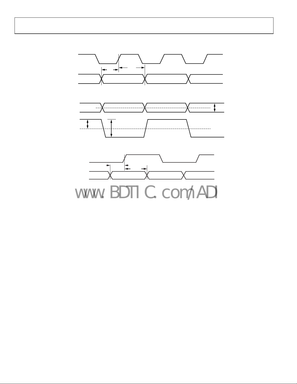
TIMING CHARACTERISTICS
CLKOUTP
t
t
S
DATAOUTP/
DATAOUTN
Figure 2. Default Mode Output Timing
OUTP
OUTN
OUTP – OUTN
V
CML
V
0V
SE
V
DIFF
Figure 3. Single-Ended vs. Differential Output Specifications
CLKOUTP/
CLKOUTN
DATAOUT P/
CLKOUTN
t
DDRS
Figure 4. Double Data Rate Mode Output Timing
H
t
DDRH
06001-002
V
SE
06001-003
06001-042
Rev. A | Page 8 of 40
ADN2817/ADN2818
www.BDTIC.com/ADI
ABSOLUTE MAXIMUM RATINGS
TA = T
C
F
Table 5.
Parameter Rating
Supply Voltage (VCC) 4.2 V
Input Voltage (All Inputs)
Junction Temperature, Maximum 125°C
Storage Temperature Range −65°C to +150°C
Lead Temperature (Soldering 10 sec) 300°C
Stresses above those listed under Absolute Maximum Ratings
may cause permanent damage to the device. This is a stress
rating only; functional operation of the device at these or any
other conditions above those indicated in the operational
section of this specification is not implied. Exposure to absolute
maximum rating conditions for extended periods may affect
device reliability.
to T
MIN
= 0.47 µF, SLICEP = SLICEN = VEE, unless otherwise noted.
Minimum VEE − 0.4 V
Maximum VCC + 0.4 V
, VCC = V
MAX
MIN
to V
, VEE = 0 V,
MAX
THERMAL CHARACTERISTICS
Thermal Resistance
32-lead LFCSP, 4-layer board with exposed paddle soldered to
VEE: θ
= 28°C/W.
JA
ESD CAUTION
Rev. A | Page 9 of 40
ADN2817/ADN2818
www.BDTIC.com/ADI
PIN CONFIGURATION AND FUNCTION DESCRIPTIONS
VBER
VCC
VEE
DATAOUTP
DATAOUTN
SQUELCH
CLKOUTP
CLKOUTN
25
26
27
28
29
31
30
32
VCC
VREF
NIN
PIN
SLICEP
SLICEN
VEE
1
2
3
4
5
6
7
8
PIN 1
INDICATOR
ADN2817/
ADN2818
TOP VIEW
(Not to Scale)
9
11
12
10
VCC
THRADJ
REFCLKP
REFCLKN
13
VEE
BERMODE
NOTES
1. EXPOSE D PADDLE ON THE BOTTOM OF THE PACKAGE
MUST BE CONNECT ED TO VEE.
24
VCC
23
VEE
22
LOS
21
SDA
20
SCK
19
SADDR5
18
VCC
17
VEE
16
15
14
CF2
CF1
LOL
06001-004
Figure 5. Pin Configuration
Table 6. Pin Function Descriptions
Pin No. Mnemonic Type1 Description
1 BERMODE DI Set this pin to logic low to enable analog voltage output mode for BER monitor.
2 VCC P Power for Input Stage, LOS.
3 VREF AO Internal VREF Voltage. Decouple to GND with a 0.1 μF capacitor.
4 NIN AI Differential Data Input. CML.
5 PIN AI Differential Data Input. CML.
6 SLICEP AI Differential Slice Level Adjust Input.
7 SLICEN AI Differential Slice Level Adjust Input.
8 VEE P GND for the Limiting Amplifier (Lim Amp), LOS.
9 THRADJ AI LOS Threshold Setting Resistor.
10 REFCLKP DI Differential REFCLK Input. 10 MHz to 200 MHz.
11 REFCLKN DI Differential REFCLK Input. 10 MHz to 200 MHz.
12 VCC P VCO Power.
13 VEE P VCO GND.
14 CF2 AO Frequency Loop Capacitor.
15 CF1 AO Frequency Loop Capacitor.
16 LOL DO Loss of Lock Indicator. Active high, LVTTL.
17 VEE P FLL Detector GND.
18 VCC P FLL Detector Power.
19 SADDR5 DI Slave Address Bit 5.
20 SCK DI I2C Clock Input.
21 SDA DI I2C Data Input.
22 LOS DO Loss of Signal Detect Output. Active high, LVTTL.
23 VEE P Output Buffer, I2C GND.
24 VCC P Output Buffer, I2C Power.
25 CLKOUTN DO Differential Recovered Clock Output. CML.
26 CLKOUTP DO Differential Recovered Clock Output. CML.
27 SQUELCH DI Disable Clock and Data Outputs. Active high, LVTLL.
28 DATAOUTN DO Differential Recovered Data Output. CML.
29 DATAOUTP DO Differential Recovered Data Output. CML.
30 VEE P Phase Detector, Phase Shifter GND.
31 VCC P Phase Detector, Phase Shifter Power.
32 VBER AO This pin represents BER when analog BERMON is enabled with 3 kΩ to VEE.
EP EPAD P Connect exposed pad to VEE. Note that the exposed pad must be connected to VEE.
1
P = power, AI = analog input, AO = analog output, DI = digital input, DO = digital output.
Rev. A | Page 10 of 40
ADN2817/ADN2818
V
www.BDTIC.com/ADI
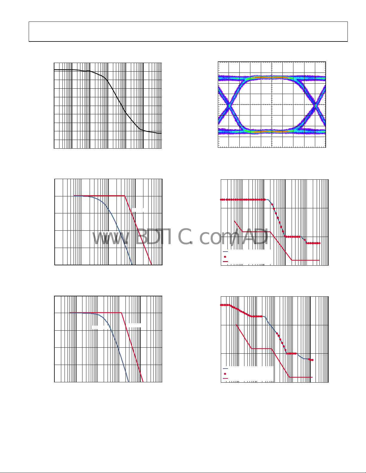
TYPICAL PERFORMANCE CHARACTERISTICS
0.020
0.018
0.016
0.014
0.012
0.010
0.008
TRIP POINT (mV p-p)
0.006
0.004
0.002
0
110100
1k 100k10k 1M
R
(Ω)
TH
Figure 6. LOS Comparator Trip Point Programming
6001-005
200mV/DI
50ps/DIV
06001-040
Figure 9. Output Eye, OC-48
5
0
–5
GAIN (dB)
–10
–15
–20
100 1k 10k 100k 1M
ADN2817
JITTER F REQUENCY (Hz)
SONET
Figure 7. Jitter Transfer, OC-1
5
0
–5
GAIN (dB)
–10
–15
–20
100 1k 10k 100k 1M 10M
ADN2817
JITTER FREQUENCY (Hz)
SONET
Figure 8. Jitter Transfer, OC-3
100
10
1
JITTER AMPL ITUDE (UI)
ADN2817
EQUIPMENT LIMIT
SONET GR-253 CORE 004
0.1
10 100 1k 10k 100k 1M
6001-032
JITTER FREQUENCY (Hz)
06001-039
Figure 10. Jitter Tolerance, OC-1
100
10
1
JITTER AMPLITUDE (UI)
ADN2817
EQUIPMENT LIMIT
SONET GR-253 CORE 004
0.1
10 100 1k 10k 100k 10M1M
06001-034
JITTER FREQUENCY (Hz)
06001-038
Figure 11. Jitter Tolerance, OC-3
Rev. A | Page 11 of 40
ADN2817/ADN2818
www.BDTIC.com/ADI
5
0
SONET
–5
GAIN (dB)
–10
–15
–20
1k 10k 100k 1M 10M
ADN2817
JITTER F REQUENCY (Hz)
Figure 12. Jitter Transfer, OC-12
5
0
SONET
–5
GAIN (dB)
–10
ADN2817
06001-033
1000
100
10
JITTER AMP LITUDE (UI)
1
ADN2817
EQUIPMENT LIMIT
SONET GR- 253 CORE 004
0.1
10 100 1k 10k 100k 10M1M
JITTER F REQUENCY (Hz)
Figure 15. Jitter Tolerance, OC-12
1000
100
10
06001-037
–15
–20
10k 100k 1M 10M 100M
JITTER FRE QUENCY (Hz)
Figure 13. Jitter Transfer, OC-48
0.70
0.65
0.60
0.55
0.50
0.45
OUTPUT SWING (V)
0.40
CLKOUTP ADN2817 BOOST
0.35
CLKOUTN ADN2817 BOOS T
CLKOUTP ADN2817 NO BOOST
CLKOUTN ADN2817 NO BO OST
0.30
100M 600M 1.1G 1.6G 2.1G 2.6G 3.1G
DATA RATE (Hz)
Figure 14. Output Swing vs. Data Rate
JITTER AMPLITUDE (UI)
1
ADN2817
EQUIPMENT LIMIT
SONET GR- 253 CORE 004
0.1
10 100 1k 10k 100k 100M10M1M
06001-035
JITTER F REQUENCY (Hz)
06001-036
Figure 16. Jitter Tolerance, OC-48
1
0.1
0.01
0.001
0.0001
0.00001
0.000001
BIT ERROR RATE
0.0000001
0.00000001
0.000000001
06001-043
1.01.52.02.53.03.54.04.5
INPUT LEVEL (mV)
06001-041
Figure 17. Bit Error Rate vs. Input Level
Rev. A | Page 12 of 40
ADN2817/ADN2818
www.BDTIC.com/ADI
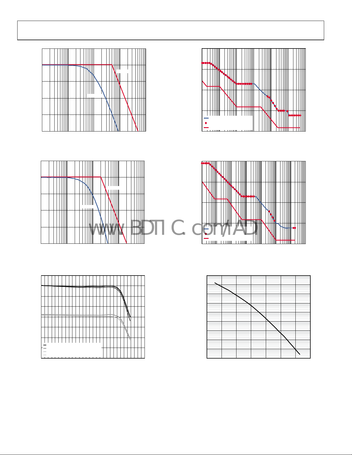
I2C INTERFACE TIMING AND INTERNAL REGISTER DESCRIPTION
SLAVE ADDRESS [6:0]
1A500000X
MSB = 1 SET BY
PIN 19
Figure 18. Slave Address Configuration
R/W
CTRL.
0 = WR
1 = RD
06001-007
S SLAVE ADDR, LSB = 0 (WR) A(S) A(S) A(S)DATASUB ADDR A(S) PDATA
Figure 19. I
2
C Write Data Transfer
06001-008
S
S = START BIT P = STOP BIT
A(S) = ACKNOWLEDG E BY SLAVE A(M) = ACKNOWLEDGE BY M ASTER
SSLAVE ADDR, LSB = 0 (WR) SLAVE ADDR, LSB = 1 (RD)A(S) A(S)SUB ADDR A(S ) DATA A(M) DATA PA(M)
A(M) = LACK OF ACKNOWLEDGE BY MASTER
Figure 20. I
2
C Read Data Transfer
6001-009
SDA
SCK
START BIT
S
SLAVE ADDRESS SUB ADDRESS DATA
SLADDR[4:0]
Figure 21. I
SUB ADDR[6:1] DATA[6:1]
2
C Data Transfer Timing
D0D7A0A7A5A6
STOP BIT
ACKACKWR ACK
P
06001-010
t
F
SDA
t
SCK
SSPS
LOW
t
HD;STA
t
R
t
HD;DAT
t
SU;DAT
Figure 22. I
t
F
t
HIGH
t
SU;STA
2
C Port Timing Diagram
t
HD;STA
t
SU;STO
t
BUF
t
R
06001-011
Rev. A | Page 13 of 40

ADN2817/ADN2818
www.BDTIC.com/ADI
Table 7. Internal Register Map
Reg Name R/W Addr D7 D6 D5 D4 D3 D2 D1 D0
FREQ0 R 0x00 MSB LSB
FREQ1 R 0x01 MSB LSB
FREQ2 R 0x02 0 MSB LSB
RATE R 0x03 COARSE_RD[8:1]
MISC R 0x04 x x LOS status Static
CTRLA W 0x08 f
CTRLA_RD R 0x05 Readback CTRLA
CTRLB W 0x09 Config
CTRLB_RD R 0x06 Readback CTRLB
CTRLC W 0x11 0 0 0 0 0 Config LOS Squelch mode 0
CTRLD W 0x22 CDR
CTRLE W 0x1F 0 0 0 0 0 PRBS/DDR enable
SEL_MODE W 0x34 0 0 0 0 0 0 CLK holdover
HI_CODE W 0x35 HI_CODE[8:1]
LO_CODE W 0x36 LO_CODE[8:1]
CODE_LSB W 0x39 0 0 0 0 0 0 HI_CODE[0] (LSB) LO_CODE[0] (LSB)
BERCTLA W 0x1E BER timer (NUMBITS) 0 BER start
BERCTLB W 0x1F 0 0 Enable
BERSTS R 0x20 x x x x x x x End of BER
BER_RES R 0x21 BER_RES[7:0], one byte of pseudo BER measurement result (NUMERRORS[39:0])
BER_DAC R 0x24 x x BER_DAC[5:0], input to BER DAC in analog BERMON mode
PHASE W 0x37 0 0 PHASE[5:0], twos compliment sample phase adjustment, PHASE code range is [−30, +30] decimal,
range Data rate/DIV_FREF ratio Measure
REF
LOL
bypass
Reset
MISC[4]
Disable
DATAOUT
buffer
Initiate freq
acquisition
Disable
CLKOUT
buffer
BERMON
which gives a sampling phase offset range of [−0.5, +0.5] UI; for example, PHASE = 111010 is
LOL
0 Reset
0 Initiate
BER
stdby
mode
−6 decimal, which gives a sampling phase offset of −6/+60 = −0.1 UI
LOL status Data rate
measurement
complete
0 0 0
MISC[2]
PRBS
sequence
Error count byte select, for example, 011 = Byte 3 of 5
pulse
0 Output mode
x COARSE_RD[0] (LSB)
Lock to REFCLK
data rate
PRBS mode
0
mode
measurement
(EOBM)
Table 8. Miscellaneous Register, MISC
LOS Status Static LOL LOL Status
D7 D6 D5 D4 D3 D2 D1 D0
x x 0 = no loss of signal 0 = waiting for next LOL 0 = locked 0 = measuring data rate x COARSE_RD[0]
1 = loss of signal 1 = static LOL until reset 1 = acquiring 1 = measurement complete
Table 9. Control Register, CTRLA
f
Range Data Rate/DIV_FREF Ratio Measure Data Rate Lock to REFCLK
REF
D7 D6 Range D5 D4 D3 D2 Ratio D1 D0
Set to 0 Set to 0 10 MHz to 25 MHz 0 0 0 0 1 Set to 1 to measure data rate 0 = lock to input data
Set to 0 Set to 1 25 MHz to 50 MHz 0 0 0 1 2 1 = lock to reference clock
Set to 1 Set to 0 50 MHz to 100 MHz 0 0 1 0 4
Set to 1 Set to 1 100 MHz to 200 MHz n 2n
1 0 0 0 256
Rev. A | Page 14 of 40
Data Rate Measurement
Complete
COAR SE_R D[0]
(LSB)

ADN2817/ADN2818
www.BDTIC.com/ADI
Table 10. Control Register, CTRLB
Config LOL Reset MISC[4] Initiate Frequency Acq Reset MISC[2]
D7 D6 D5 D4 D3 D2 D1 D0
0 = LOL pin normal operation
1 = LOL pin is static LOL
Table 11. Control Register, CTRLC
D7 D6 D5 D4 D3 D2 D1 D0
Set to 0 Set to 0 Set to 0 Set to 0 Set to 0 0 = active high LOS 0 = squelch CLK and DATA Set to 0
Table 12. Control Register, CTRLD
Disable
CDR Bypass
D7 D6 D5 D4 D3 D2 D1 D0 Function
0 = CDR enabled 0 = data buffer enabled 0 = CLK buffer enabled Set to 0
1 = CDR disabled 1 = data buffer disabled 1 = CLK buffer disabled 0 0 1 Generate mode
DATAOUT Buffer
Write a 1 followed
by 0 to reset MISC[4]
Disable
CLKOUT Buffer
Write a 1 followed
by 0 to initiate a
frequency acquisition
Configure LOS Squelch Mode
1 = active low LOS 1 = squelch CLK or DATA
Set
to 0
Initiate PRBS
Sequence PRBS Mode
Write a 1 followed
by 0 to initiate a
PRBS generate
sequence
Write a 1 followed
by 0 to reset MISC[2]
0 0 0 Power-down PRBS
1 0 0 Detect mode
Set
to 0
Set
to 0
Set
to 0
Table 13. Control Register, CTRLE
PRBS/DDR Enable
D7 D6 D5 D4 D3 D2 D1 D0 Function
Set to 0 Set to 0 Set to 0 Set to 0 Set to 0 0 1 0 Enable DDR mode (double data rate mode)
1 0 1 Enable PRBS detector/generator
All other combinations reserved
Table 14. SEL_MODE
CLK Holdover Mode
D7 D6 D5 D4 D5 D2 D1 D0
Set to 0 Set to 0 Set to 0 Set to 0 Set to 0 Set to 0 Set to 1 for clock holdover mode Set to 0
Table 15. BERCTLA
Error Count Byte Select
BER Timer (NUMBITS) BER Start Pulse
D7 D6 D5 No. of Bits D4 D3 D2 D1 D0 Byte Selection
0 0 0 218 bits Set to 0 Write a 1 followed by a 0 to initiate BER measurement 0 0 0 Byte 0
0 0 1 221 bits 0 0 1 Byte 1
0 1 0 224 bits 0 1 0 Byte 2
0 1 1 227 bits 0 1 1 Byte 3
1 0 0 230 bits 1 0 0 Byte 4
1 0 1 233 bits 1 0 1 Byte 5
1 1 0 236 bits
1 1 1 239 bits
(NUMERRORS[39:0])
Rev. A | Page 15 of 40
ADN2817/ADN2818
www.BDTIC.com/ADI
Table 16. BERCTLB
Enable BERMON BER Standby Mode Output Mode
D7 D6 D5 D4 D3 D2 D1 D0 Mode
Set to 0 Set to 0 0 = BER disabled 0 = BER measurement enabled Set to 0 0 0 0
1 = BER enabled 1 = BER measurement in standby mode
0 0 1
0 1 0
0 1 1
1
NDC = normal decision circuit data and clock, ODC = offset decision circuit data and clock, DIV0 = normal decision circuit data and half rate clock, DIV1 = offset
decision circuit data and half rate clock, → OB indicates that the referenced signals are routed to the data and clock chip output buffers.
NDC → OB
ODC → OB
DIV0 → OB
DIV1 → OB
1
1
1
1
Rev. A | Page 16 of 40
ADN2817/ADN2818
p
p
www.BDTIC.com/ADI
TERMINOLOGY
INPUT SENSITIVITY AND INPUT OVERDRIVE
Sensitivity and overdrive specifications for the quantizer involve
offset voltage, gain, and noise. The relationship between the logic
output of the quantizer and the analog voltage input is shown in
Figure 23. For sufficiently large positive input voltages, the output is
always Logic 1 and, similarly for negative inputs, the output is
always Logic 0. However, the transitions between Output Logic
Level 1 and Output Logic Level 0 are not at precisely defined
input voltage levels but occur over a range of input voltages. Within
this range of input voltages, the output might be either 1 or 0, or
it might even fail to attain a valid logic state. The width of this
zone is determined by the input voltage noise of the quantizer.
The center of the zone is the quantizer input offset voltage. Input
overdrive is the magnitude of signal required to guarantee the
correct logic level with 1 × 10
OUTPUT
−10
confidence level.
1
0
OFFSET
OVERDRIVE
NOISE
INPUT (V p-p)
10mV p-
SCOPE
PROBE
PIN
VREF
Figure 24. Single-Ended Sensitivity Measurement
+
QUANTIZER
–
50Ω50Ω
3kΩ
VREF
2.5V
06001-013
Differentially driving the ADN2817 (see Figure 25), sensitivity
seems to improve from observing the quantizer input with an
oscilloscope probe. This is an illusion caused by the use of a singleended probe. A 5 mV p-p signal appears to drive the ADN2817
quantizer. However, the single-ended probe measures only half
the signal. The true quantizer input signal is twice this value
because the other quantizer input is a complementary signal to
the signal being observed.
5mV p-
VREF
SCOPE
PROBE
SENSITIVITY
(2× OVERDRIVE )
Figure 23. Input Sensitivity and Input Overdrive
06001-012
SINGLE-ENDED vs. DIFFERENTIAL
AC coupling is typically used to drive the inputs to the quantizer.
The inputs are internally dc biased to a common-mode potential
of ~2.5 V. Driving the ADN2817/ADN2818 single-ended and
observing the quantizer input with an oscilloscope probe at the
point indicated in Figure 24 shows a binary signal with an average
value equal to the common-mode potential and instantaneous
values both above and below the average value. It is convenient
to measure the peak-to-peak amplitude of this signal and call
the minimum required value the quantizer sensitivity. Referring
to Figure 24, because both positive and negative offsets need to
be accommodated, the sensitivity is twice the overdrive. The
ADN2817 quantizer typically has 5 mV p-p sensitivity. The
ADN2818 does not have a limiting amplifier at its input. The
input sensitivity for the ADN2818 is 200 mV p-p.
VREF
PIN
NIN
VREF
5mV p-p
Figure 25. Differential Sensitivity Measurement
50Ω
+
QUANTIZER
–
50Ω
3kΩ
2.5V
06001-014
LOS RESPONSE TIME
The LOS response time is the delay between the removal of the
input signal and the indication of the loss of signal at the LOS
output, Pin 22. When the inputs are dc-coupled, the LOS assert
time of the ADN2817 is 450 ns typically and the deassert time is
500 ns typically. In practice, the time constant produced by the
ac coupling at the quantizer input and the 50 Ω on-chip input
termination determine the LOS response time.
Rev. A | Page 17 of 40

ADN2817/ADN2818
R
www.BDTIC.com/ADI
JITTER SPECIFICATIONS
The ADN2817/ADN2818 CDR is designed to achieve the best
bit error rate (BER) performance and exceeds the jitter transfer,
generation, and tolerance specifications proposed for SONET/SDH
equipment defined in the Telcordia® Technologies specification.
Jitter is the dynamic displacement of digital signal edges from
their long-term average positions, measured in unit intervals
(UI), where 1 UI = 1 bit period. Jitter on the input data can cause
dynamic phase errors on the recovered clock sampling edge. Jitter
on the recovered clock causes jitter on the retimed data.
The following sections briefly summarize the specifications
of jitter generation, transfer, and tolerance in accordance with
the Telcordia document (GR-253-CORE, Issue 3, September
2000) for the optical interface at the equipment level and the
ADN2817/ADN2818 performance with respect to those
specifications.
JITTER GENERATION
The jitter generation specification limits the amount of jitter
that can be generated by the device with no jitter and wander
applied at the input. For OC-48 devices, the band-pass filter
has a 12 kHz high-pass cutoff frequency with a roll-off of
20 dB/decade and a low-pass cutoff frequency of at least
20 MHz. The jitter generated must be less than 0.01 UI rms
and must be less than 0.1 UI p-p.
0.1
SLOPE = –20dB/DE CADE
JITTER GAIN (dB)
ACCEPTABLE
RANGE
JITTER FREQUENCY ( kHz)
Figure 26. Jitter Transfer Curve
f
C
JITTER TOLERANCE
The jitter tolerance is defined as the peak-to-peak amplitude of
the sinusoidal jitter applied on the input signal, which causes a
1 dB power penalty. This is a stress test intended to ensure that
no additional penalty is incurred under the operating conditions
(see Figure 27).
15.00
SLOPE = –20d B/DECADE
6001-015
JITTER TRANSFER
The jitter transfer function is the ratio of the jitter on the output
signal to the jitter applied on the input signal vs. the frequency.
This parameter measures the limited amount of the jitter on
an input signal that can be transferred to the output signal
(see Figure 26).
1.50
AMPLITUDE (UI p-p)
0.15
INPUT JITTE
f
0
Figure 27. SONET Jitter Tolerance Mask
f
1
JITTER F REQUENCY (kHz)
f
2f3
f
4
06001-016
Rev. A | Page 18 of 40

ADN2817/ADN2818
p
G
www.BDTIC.com/ADI
THEORY OF OPERATION
The ADN2817/ADN2818 are delay- and phase-locked loop
circuits for clock recovery and data retiming from an NRZ
encoded data stream. The phase of the input data signal is tracked
by two separate feedback loops that share a common control
voltage. A high speed delay-locked loop path uses a voltage
controlled phase shifter to track the high frequency components
of input jitter. A separate phase control loop, comprised of the
VCO, tracks the low frequency components of input jitter. The
initial frequency of the VCO is set by a third loop, which
compares the VCO frequency with the input data frequency
and sets the coarse tuning voltage. The jitter tracking phaselocked loop controls the VCO by the fine-tuning control.
The delay- and phase-locked loops together track the phase of
the input data signal. For example, when the clock lags input
data, the phase detector drives the VCO to a higher frequency
and increases the delay through the phase shifter; both of these
actions serve to reduce the phase error between the clock and
data. The faster clock picks up phase, while, simultaneously, the
delayed data loses phase. Because the loop filter is an integrator,
the static phase error is driven to zero.
Another view of the circuit is that the phase shifter implements
the zero required for frequency compensation of a second-order
phase-locked loop, and this zero is placed in the feedback path
and, thus, does not appear in the closed-loop transfer function.
Jitter peaking in a conventional second-order phase-locked loop
is caused by the presence of this zero in the closed-loop transfer
function. Because this circuit has no zero in the closed-loop
transfer, jitter peaking is minimized.
The delay- and phase-locked loops together simultaneously
provide wideband jitter accommodation and narrow-band jitter
filtering. The linearized block diagram in
Figure 28 shows that
the jitter transfer function, Z(s)/X(s), is second-order low-pass,
providing excellent filtering. Note that the jitter transfer has no
zero, unlike an ordinary second-order phase-locked loop. This
means that the main PLL loop has virtually zero jitter peaking
(see Figure 29). This makes this circuit ideal for signal regenerator applications, where jitter peaking in a cascade of regenerators
can contribute to hazardous jitter accumulation.
The error transfer, e(s)/X(s), has the same high-pass form as an
ordinary phase-locked loop. This transfer function is free to be
optimized to give excellent wideband jitter accommodation,
because the jitter transfer function, Z(s)/X(s), provides the
narrow-band jitter filtering.
X(s)
INPUT
DATA
RECOVERED
CLOCK
d = PHASE DETECTOR GAIN
o = VCO GAIN
c = LOOP INTEGRATOR
sh = PHASE SHIF TER GAIN
n = DIVIDE RATIO
Figure 28. ADN2817/ADN2818 PLL/DLL Architecture
JITTER G AIN (dB)
Figure 29. ADN2817/ADN2818 Jitter Response vs. Conventional PLL
The delay- and phase-locked loops contribute to overall jitter
accommodation. At low frequencies of input jitter on the data
signal, the integrator in the loop filter provides high gain to track
large jitter amplitudes with small phase error. In this case, the
VCO is frequency modulated and jitter is tracked as in an ordinary
phase-locked loop. The amount of low frequency jitter that can
be tracked is a function of the VCO tuning range. A wider tuning
range gives larger accommodation of low frequency jitter. The
internal loop control voltage remains small for small phase
errors, so the phase shifter remains close to the center of its
range and thus contributes little to the low frequency jitter
accommodation.
Z(s)
n psh
psh
e(s)
d/sc
JITTER T RANSFER FUNCTI ON
Z(s)
=
X(s)
2
s
TRACKING ERROR T RANSFER FUNCTI ON
e(s)
=
X(s)
2
s
o
d psh
FREQUENCY ( kHz)
o/s
1/n
1
n psh
cn
s + 1
+
o
do
2
s
d psh
do
s++
c
cn
JITTER PEAKIN
IN ORDINARY PLL
c
ADN28xx
Z(s)
X(s)
06001-017
06001-018
Rev. A | Page 19 of 40

ADN2817/ADN2818
www.BDTIC.com/ADI
At medium jitter frequencies, the gain and tuning range of the
VCO are not large enough to track input jitter. In this case, the
VCO control voltage becomes large and saturates, and the VCO
frequency dwells at one extreme of its tuning range or the other.
The size of the VCO tuning range, therefore, has only a small
effect on the jitter accommodation. The delay-locked loop control
voltage is now larger, and so the phase shifter takes on the
burden of tracking the input jitter. The phase shifter range, in
UI, can be seen as a broad plateau on the jitter tolerance curve.
The phase shifter has a minimum range of 2 UI at all data rates.
The gain of the loop integrator is small for high jitter frequencies,
so that larger phase differences are needed to make the loop
control voltage big enough to tune the range of the phase shifter.
Large phase errors at high jitter frequencies cannot be tolerated.
In this region, the gain of the integrator determines the jitter
accommodation. Because the gain of the loop integrator declines
linearly with frequency, jitter accommodation is lower with higher
jitter frequency. At the highest frequencies, the loop gain is very
small, and little tuning of the phase shifter can be expected. In this
case, jitter accommodation is determined by the eye opening of the
input data, the static phase error, and the residual loop jitter
generation. The jitter accommodation is roughly 0.5 UI in this
region. The corner frequency between the declining slope and
the flat region is the closed-loop bandwidth of the delay-locked
loop, which is roughly 3 MHz at OC-48.
Rev. A | Page 20 of 40
ADN2817/ADN2818
www.BDTIC.com/ADI
FUNCTIONAL DESCRIPTION
FREQUENCY ACQUISITION
The ADN2817/ADN2818 acquire frequency from the data over
a range of data frequencies from 10 Mbps to 2.7 Gbps. The lock
detector circuit compares the frequency of the VCO and the
frequency of the incoming data. When these frequencies differ
by more than 1000 ppm, LOL is asserted. This initiates a frequency acquisition cycle. The VCO frequency is reset to the
bottom of its range, which is 10 MHz. The frequency detector
compares this VCO frequency and the incoming data frequency
and increments the VCO frequency, if necessary. Initially, the
VCO frequency is incremented in large steps to aid fast acquisition. As the VCO frequency approaches the data frequency, the
step size is reduced until the VCO frequency is within 250 ppm
of the data frequency, at which point LOL is deasserted.
Once LOL is deasserted, the frequency-locked loop is turned off.
The phase- and delay-locked loop (PLL/DLL) pulls in the VCO
frequency until the VCO frequency equals the data frequency.
The frequency loop requires a single external capacitor between
CF1 and CF2, Pin 14 and Pin 15. A 0.47 µF ± 20%, X7R ceramic
chip capacitor with <10 nA leakage current is recommended.
Leakage current of the capacitor can be calculated by dividing
the maximum voltage across the 0.47 µF capacitor, ~3 V, by the
insulation resistance of the capacitor. The insulation resistance
of the 0.47 F capacitor should be greater than 300 MΩ.
LOCK DETECTOR OPERATION
The lock detector on the ADN2817/ADN2818 has three modes
of operation: normal mode, REFCLK mode, and static LOL mode.
Normal Mode
In normal mode, the ADN2817/ADN2818 function as continuous
rate CDRs that lock onto any data rate from 10 Mbps to 2.7 Gbps
without the use of a reference clock as an acquisition aid. In this
mode, the lock detector monitors the frequency difference between
the VCO and the input data frequency, and deasserts the loss of
lock signal that appears on LOL (Pin 16) when the VCO is within
250 ppm of the data frequency. This enables the delay- and phaselocked loop (DLL/PLL), which pulls the VCO frequency in the
remaining amount and acquires phase lock. When locked, if the
input frequency error exceeds 1000 ppm (0.1%), the loss of lock
signal is reasserted and control returns to the frequency loop,
which begins a new frequency acquisition starting at the lowest
point in the VCO operating range, 10 MHz. The LOL pin remains
asserted until the VCO locks onto a valid input data stream to
within 250 ppm frequency error. This hysteresis is shown in
Figure 30.
–1000
Figure 30. Transfer Function of LOL
LOL Detector Operation Using a Reference Clock
In this mode, a reference clock is used as an acquisition aid to
lock the ADN2817/ADN2818 VCO. Lock to reference mode is
enabled by setting CTRLA[0] to 1. The user also needs to write
to the CTRLA[7:6] and CTRLA[5:2] bits to set the reference
frequency range and the divide ratio of the data rate with respect
to the reference frequency. For more details, see the Reference
Clock (Optional) section. In this mode, the lock detector monitors
the difference in frequency between the divided down VCO and
the divided down reference clock. The loss of lock signal, which
appears on the LOL (Pin 16), is deasserted when the VCO is
within 250 ppm of the desired frequency. This enables the DLL/
PLL, which pulls the VCO frequency in the remaining amount
with respect to the input data and acquires phase lock. Once
locked, if the input frequency error exceeds 1000 ppm (0.1%),
the loss of lock signal is reasserted and control returns to the
frequency loop, which reacquires with respect to the reference
clock. The LOL pin remains asserted until the VCO frequency is
within 250 ppm of the desired frequency. This hysteresis is shown
in Figure 30.
Static LOL Mode
The ADN2817/ADN2818 implement a static LOL feature, which
indicates if a loss of lock condition has ever occurred and remains
asserted, even if the ADN2817/ADN2818 regain lock, until the
static LOL bit is manually reset. I
static LOL bit. If there is ever an occurrence of a loss of lock
condition, this bit is internally asserted to logic high. The MISC[4]
bit remains high even after the ADN2817/ADN2818 reacquire
lock to a new data rate. This bit can be reset by writing a 1 followed
by 0 to I
2
C Register Bit CTRLB[6]. When reset, the MISC[4] bit
remains deasserted until another loss of lock condition occurs.
Writ i ng a 1 t o I
2
C Register Bit CTRLB[7] causes the LOL pin,
Pin 16, to become a static LOL indicator. In this mode, the LOL
pin mirrors the contents of the MISC[4] bit and has the functionality described in the previous paragraph. The CTRLB[7] bit
defaults to 0. In this mode, the LOL pin operates in the normal
operating mode, that is, it is asserted only when the ADN2817/
ADN2818 are in acquisition mode and deasserts when the
ADN2817/ADN2818 reacquire lock.
LOL
1
0–250 250 1000 f
2
C Register Bit MISC[4] is the
VCO
(ppm)
ERROR
06001-019
Rev. A | Page 21 of 40
ADN2817/ADN2818
www.BDTIC.com/ADI
HARMONIC DETECTOR
The ADN2817/ADN2818 provide a harmonic detector, which
detects whether the input data has changed to a lower harmonic
of the data rate onto which the VCO is currently locked. For
example, if the input data instantaneously changes from an OC-48,
2.488 Gbps to an OC-12, 622.080 Mbps bit stream, this could be
perceived as a valid OC-48 bit stream, because the OC-12 data
pattern is exactly 4× slower than the OC-48 pattern. Therefore,
if the change in data rate is instantaneous, a 101 pattern at OC-12 is
perceived by the ADN2817/ADN2818 as a 111100001111 pattern
at OC-48. If the change to a lower harmonic is instantaneous, a
typical CDR could remain locked at the higher data rate.
The ADN2817/ADN2818 implement a harmonic detector that
automatically identifies whether the input data has switched to a
lower harmonic of the data rate onto which the VCO is currently
locked. When a harmonic is identified, the LOL pin is asserted
and a new frequency acquisition is initiated. The ADN2817/
ADN2818 automatically lock onto the new data rate, and the
LOL pin is deasserted.
However, the harmonic detector does not detect higher harmonics of the data rate. If the input data rate switches to a
higher harmonic of the data rate onto which the VCO is currently
locked, the VCO loses lock, the LOL pin is asserted, and a new
frequency acquisition is initiated. The ADN2817/ ADN2818
automatically lock onto the new data rate.
The time to detect lock to harmonic is
16,384 × (T
d
/ρ)
where:
1/T
is the new data rate. For example, if the data rate is switched
d
from OC-48 to OC-12, then T
= 1/622 MHz.
d
ρ is the data transition density. Most coding schemes seek to
ensure that ρ = 0.5, for example, PRBS or 8b/10b encoding.
When the ADN2817/ADN2818 is placed in lock to reference
mode, the harmonic detector is disabled.
LIMITING AMPLIFIER (ADN2817 ONLY)
The limiting amplifier on the ADN2817 has differential inputs
(PIN/NIN) that internally terminate with 50 Ω to an on-chip
voltage reference (VREF = 2.5 V typically). The inputs are typically
ac-coupled externally, although dc coupling is possible as long
as the input common-mode voltage remains above 2.5 V (see
Figure 40, Figure 41, and Figure 42). Input offset is factory
trimmed to achieve better than 6 mV typical sensitivity with
minimal drift. The limiting amplifier can be driven differentially
or single-ended.
Rev. A | Page 22 of 40
SLICE LEVEL ADJUST (ADN2817 ONLY)
The quantizer slicing level can be offset by ±100 mV to mitigate
the effect of amplified spontaneous emission (ASE) noise or duty
cycle distortion by applying a differential voltage input of up to
±0.95 V to SLICEP/SLICEN inputs. If no adjustment of the slice
level is needed, SLICEP/SLICEN should be tied to VEE. The gain
of the slice adjustment is ~0.1 V/V.
LOSS OF SIGNAL (LOS) DETECTOR (ADN2817 ONLY)
The receiver front end LOS detector circuit detects when the input
signal level has fallen below a user-adjustable threshold. The
threshold is set with a single external resistor from Pin 9, THRADJ,
to VEE. The LOS comparator trip point vs. resistor value is shown
in Figure 6. If the input level to the ADN2817 drops below the
programmed LOS threshold, the output of the LOS detector, Pin 22
(LOS), is asserted to a Logic 1. The LOS detector response time is
450 ns by design but is dominated by the RC time constant in accoupled applications. The LOS pin defaults to active high.
However, by setting Bit CTRLC[2] to 1, the LOS pin is configured
as active low.
There is typically 6 dB of electrical hysteresis designed into the
LOS detector to prevent chatter on the LOS pin. This means that,
if the input level drops below the programmed LOS threshold
causing the LOS pin to assert, the LOS pin is not deasserted until
the input level has increased to 6 dB (2×) above the LOS threshold
(see Figure 31).
LOS OUTPUT
)
DIFF
INPUT VOLTAGE (V
Figure 31. ADN2817 LOS Detector Hysteresis
The LOS detector and the slice level adjust can be used simultaneously on the ADN2817. This means that any offset added to
the input signal by the slice adjust pins does not affect the LOS
detector measurement of the absolute input level.
INPUT LEVEL
HYSTERESIS
LOS THRESHOLD
06001-020
t

ADN2817/ADN2818
www.BDTIC.com/ADI
SAMPLE PHASE ADJUST
If the user is not using the BER monitoring function, sample
phase adjustment can be used to optimize the horizontal sampling point of the incoming data eye. The ADN2817 automatically
centers the sampling point to the best of its ability. However,
sample phase adjustment can be used to compensate for any
static phase offset of the CDR and data eye jitter profile asymmetry.
Sample phase adjustment is applied to the incoming eye via the
phase register. The sampling phase can be adjusted by ±0.5 UI,
in 6 degree steps, relative to the normal CDR data sampling
instant. Using the sample phase adjustment capability uses an
additional 160 mW of power. The AN-941 application note
gives additional information on the use of this feature.
BIT ERROR RATE (BER) MONITOR
The ADN2817 has a BER measurement feature that estimates
the actual bit error rate of the IC. This feature also allows data
eye jitter profiling and Q-factor estimation.
By knowing the BER at a sampling phase offset from the ideal
sampling phase (known as pseudo BER [PBER] values), it is
possible to extrapolate to obtain an estimate of the BER at the
actual sampling instant. This extrapolation relies on the assumption
that the input jitter is composed of deterministic and random
(Gaussian) components. The implementation requires off-chip
control and data processing to estimate the actual BER. A lower
accuracy voltage output mode is also supported that requires no
data processing or I
Brief Overview of Modes of Operation
The following two modes of operation are available for the BER
feature: the BER extrapolation mode and the voltage output mode.
Only one mode can be operational at a time. The BER extrapolation mode scans the input eye in the range of ±0.5 UI of the
data center and reads the measured PBER over the I
then applies a data processing algorithm to determine the BER.
Using the BER feature in this way provides for the greatest accuracy
in BER estimation as the magnitude of both random (Gaussian)
jitter and deterministic jitter can be estimated and used to predict
the actual BER.
In the voltage output mode, the part autonomously samples the
PBER at 0.1 UI offset and decodes this value to provide an estimate
of the input BER. This estimate is output via a DAC as an analog
current output. The AN-941 application note gives detailed
information on the use of the BER monitor features.
BER Extrapolation Mode
Power Saving
The following three power settings are available in BER
extrapolation mode: BER off, BER on, and BER standby.
In BER off mode (BERCTLB[5] = 0), the BER circuitry is
powered down with the ADN2817 providing normal CDR
operation.
2
C control.
2
C. The user
In BER on mode (BERCTLB[5] = 1), the internal BER circuitry
is powered up. The user can perform pseudo BER measurements
through the I
In BER standby mode (BERCTLB[5:4] = 11b), the BER is placed
into a lower power mode. This setting can only be set after
applying the BER on setting.
These modes are defined to allow optimal power saving
opportunities. It is not possible to switch between the BER
off setting and the BER on setting without losing lock. Switching
between the BER standby setting and the BER on setting is
achieved without interrupting data recovery. The incremental
power between the BER off setting and the BER standby setting
is 77 mW and between the BER off setting and the BER on setting
it is 160 mW.
2
C.
BER On Mode
The BER on mode allows the user to scan the incoming data eye
in the time dimension and build up a profile of the BER statistics.
The following is a brief overview of user protocol:
• The user powers up BER circuitry through I
• The user initiates the PBER measurement. Sample phase offset
and number of data bits to be counted (NUMBITS is a choice
between 2
through I
• The user initiates the pseudo BER measurement by writing a
1-to-0 transition on BERCTLA[3].
• BER logic indicates the end of the BER measurement with an
EOBM signal and updates the number of counted errors on
NUMERRORS[39:0]. The user must poll the I2C to determine
if the EOBM bit, BERSTS[0], has been asserted.
• The user reads back NUMERRORS[39:0] through the I
NUMERRORS[39:0] is read back through the 8-bit register
BER_RES at Address 0x21. The user sets BERCTLA[2:0] to
address one of the five NUMERRORS bytes and then reads the
selected byte from BER_RES.
• PBER for programmed sample phase is calculated as
numerrors/numbits.
• The user initiates another PBER measurement.
• The user sweeps the phase over −0.5 UI to +0.5 UI with respect
to the normal sampling instant to get the BER profile required.
The ADN2817 does not output the BER at the normal decision
instant. It outputs PBER measurements to the left and right of
the normal decision instants from which the user must calculate
what the BER is at the normal decision instant. A microprocessor is
required to parse the data and to use the remaining data for
BER estimation. Suitable algorithms are suggested in the BER
Monitor User Guide, AN-941.
18
, 221, 224, 227, 230, 233, 236, or 239) are supplied by user
2
C.
2
C.
2
C.
Rev. A | Page 23 of 40

ADN2817/ADN2818
www.BDTIC.com/ADI
Voltage Output Mode of Operation
A second mode of operation is the voltage output mode. This
mode is to give easy access to a coarse estimate of the BER. The
functionality is similar to that already described except that the
measurement is performed autonomously by the ADN2817,
and the result is output as a voltage on a pin from which the
actual BER can be inferred. Because this mode does not perform
scanning of the eye to separate out deterministic jitter from
random jitter effects, this method is less accurate under normal
applied jitter conditions.
The user merely has to bring the BERMODE pin low and read
the voltage on the VBER pin (see Figure 32). Alternatively, a 6bit value can be read over the I
0.9
0.7
0.5
0.3
0.1
VBER PIN VOLTAGE RELATIVE TO VEE (V)
0.001 0. 00001 0.0000001 0.000000001
Figure 32. VBER vs. Bit Error Rate
2
C
VBER VOLTAG E IS
GUARANTEED TO
SATURATE FOR
INPUT BERs LESS
THAN 0.000000001
VBER VOLTAGE IS
GUARANTEED TO
SATURATE FOR
INPUT BERs
GREATER THAN 0.001
LOG (BER)
06001-024
SQUELCH MODE
Two squelch modes are available with the ADN2817/ADN2818:
squelch DATAOUT and CLKOUT mode, and squelch DATAOUT
or CLKOUT mode.
Squelch DATAOUT and CLKOUT mode is selected when
CTRLC[1] = 0 (default mode). In this mode, when the squelch
input, Pin 27, is driven to a TTL high state, both the clock and
data outputs are set to the zero state to suppress downstream
processing. If the squelch function is not required, Pin 27 should
be tied to VEE.
Squelch DATAOUT or CLKOUT mode is selected when
CTRLC[1] is 1. In this mode, when the squelch input is driven
to a high state, the DATAOUT pins are squelched. When the
squelch input is driven to a low state, the CLKOUT pins are
squelched. This is especially useful in repeater applications,
where the recovered clock may not be needed.
I2C INTERFACE
The ADN2817/ADN2818 supports a 2-wire, I2C-compatible
serial bus driving multiple peripherals. Two inputs, serial data
(SDA) and serial clock (SCK), carry information between any
devices connected to the bus. Each slave device is recognized by
a unique address. The ADN2817/ADN2818 have two possible
7-bit slave addresses for both read and write operations. The
MSB of the 7-bit slave address is factory programmed to 1. Bit 5
of the slave address is set by Pin 19, SADDR5. Slave Address
Bits[4:0] are defaulted to all 0s. The slave address consists of the
7 MSBs of an 8-bit word. The LSB of the word either sets a read
or write operation (see Figure 18). Logic 1 corresponds to a read
operation and Logic 0 corresponds to a write operation.
To control the device on the bus, the following protocol must be
followed. First, the master initiates a data transfer by establishing
a start condition, defined by a high-to-low transition on SDA
while SCK remains high. This indicates that an address/data
stream follows. All peripherals respond to the start condition
and shift the next eight bits (the 7-bit address and the R/
The bits are transferred from MSB to LSB. The peripheral that
recognizes the transmitted address responds by pulling the
data line low during the ninth clock pulse. This is known as an
acknowledge bit. All other devices withdraw from the bus at
this point and maintain an idle condition. The idle condition is
where the device monitors the SDA and SCK lines waiting for
the start condition and correct transmitted address. The R/
bit determines the direction of the data. Logic 0 on the LSB of
the first byte means that the master writes information to the
peripheral. Logic 1 on the LSB of the first byte means that the
master reads information from the peripheral.
The ADN2817/ADN2818 act as standard slave devices on the
bus. The data on the SDA pin is eight bits long, supporting the
7-bit addresses plus the R/
W
bit. The ADN2817/ADN2818 have
eight subaddresses to enable the user-accessible internal registers
Tabl e 1 Tab l e 8
(see through ). It, therefore, interprets the first
byte as the device address and the second byte as the starting
subaddress. Auto-increment mode is supported, allowing data
to be read from, or written to, the starting subaddress and each
subsequent address without manually addressing the subsequent
subaddress. A data transfer is always terminated by a stop
condition. The user can also access any unique subaddress
register on a one-by-one basis without updating all registers.
Stop and start conditions can be detected at any stage of the
data transfer. If these conditions are asserted out of sequence
with normal read and write operations, they cause an immediate
jump to the idle condition. During a given SCK high period, the
user should issue one start condition, one stop condition, or a
single stop condition followed by a single start condition. If an
invalid subaddress is issued by the user, the ADN2817/ADN2818
do not issue an acknowledge and return to the idle condition.
W
bit).
W
Rev. A | Page 24 of 40

ADN2817/ADN2818
V
www.BDTIC.com/ADI
If the user exceeds the highest subaddress while reading back in
auto-increment mode, the highest subaddress register contents
continue to be output until the master device issues a no
acknowledge. This indicates the end of a read. In a no acknowledge
condition, the SDATA line is not pulled low on the ninth pulse.
See Figure 19 and Figure 20 for sample read and write data
transfers and Figure 21 for a more detailed timing diagram.
REFERENCE CLOCK (OPTIONAL)
A reference clock is not required to perform clock and data
recovery with the ADN2817/ADN2818. However, support for
an optional reference clock is provided. The reference clock can
be driven differentially or single-ended. If the reference clock is not
used, tie REFCLKP to VCC, and either leave REFCLKN floating or
tie it to VEE (the inputs are internally terminated to VCC/2). See
Figure 33 through Figure 35 for sample configurations.
The REFCLK input buffer accepts any differential signal with a
peak-to-peak differential amplitude of greater than 100 mV (for
example, LVPECL or LVDS) or a standard single-ended low
voltage TTL input, providing maximum system flexibility. Phase
noise and duty cycle of the reference clock are not critical and
100 ppm accuracy is sufficient.
ADN2817/ADN2818
REFCLKP
10
11
REFCLKN
Figure 33. Differential REFCLK Configuration
VCC
OUT
REFCLKP
10
REFCLKN
11
CLK
OSC
Figure 34. Single-Ended REFCLK Configuration
BUFFER
100kΩ100kΩ
VCC/2
ADN2817/ADN2818
BUFFER
100kΩ100kΩ
VCC/2
06001-021
06001-022
Rev. A | Page 25 of 40
ADN2817/ADN2818
CC
REFCLKP
10
REFCLKN
11
Figure 35. No REFCLK Configuration
BUFFER
100kΩ100kΩ
VCC/2
06001-023
The two uses of the reference clock are mutually exclusive. The
reference clock can be used either as an acquisition aid for the
ADN2817/ADN2818 to lock onto data, or to measure the frequency of the incoming data to within 0.01%. (There is the
capability to measure the data rate to approximately ±10%
without the use of a reference clock.) The modes are mutually
exclusive because, in the first use, the user knows exactly what
the data rate is and wants to force the part to lock onto only that
data rate; in the second use, the user does not know what the
data rate is and wants to measure it.
Lock to reference mode is enabled by writing 1 to I
2
C Register
Bit CTRLA[0]. Fine data rate readback mode is enabled by
writing 1 to I
2
C Register Bit CTRLA[1]. Writing a 1 to both
of these bits at the same time causes an indeterminate state
and is not supported.
Using the Reference Clock to Lock onto Data
Writing CTRLA[0] = 1 puts the ADN2817/ADN2818 into lock
to REFCLK (LTR) mode. In this mode, the ADN2817/ADN2818
lock onto a frequency derived from the reference clock according
to the following equation:
Data Rate/2
CTRLA[5:2]
= REFCLK/2
CTRLA[7:6]
The user must know exactly what the data rate is and provide
a reference clock that is a function of this rate. The ADN2817/
ADN2818 can still be used as continuous rate devices in this
configuration if a reference clock with a variable frequency is
provided (see Application Note AN-632).
The reference clock can be anywhere between 10 MHz and
200 MHz. By default, the ADN2817/ADN2818 expect a reference
clock of between 10 MHz and 25 MHz. If it is between 25 MHz
and 50 MHz, 50 MHz and 100 MHz, or 100 MHz and 200 MHz,
the user needs to configure the ADN2817/ADN2818 to use the
correct reference frequency range by setting two bits of the
CTRLA register, CTRLA[7:6].
Table 17. CTRLA[7:6] (f
Ratio) Settings
(f
REF
Range) with CTRLA[5:2]
REF
CTRLA[7:6] Range (MHz) CTRLA[5:2] Ratio
00 10 to 25 0000 1
01 25 to 50 0001 2
10 50 to 100 n
2n
11 100 to 200 1000 256

ADN2817/ADN2818
www.BDTIC.com/ADI
The user can specify a fixed integer multiple of the reference
clock to lock onto using CTRLA[5:2], where CTRLA should be
set to the data rate/DIV_FREF and DIV_FREF represents the
divided-down reference referred to the 10 MHz to 25 MHz band.
For example, if the reference clock frequency is 38.88 MHz and
the input data rate is 622.08 Mbps, then CTRLA[7:6] is set to
[01] to give a divided-down reference clock of 19.44 MHz.
CTRLA[5:2] is set to [0101], that is, 5, because
622.08 Mbps/19.44 MHz = 2
5
When the CTRLA[7:2] value is correct and CTRLA[0] has been
written to a Logic 1, it is recommended that a 1-to-0 transition
be written to CTRLB[5] to initiate a new frequency acquisition
with respect to the reference clock.
In this mode, if the ADN2817/ADN2818 lose lock for any
reason, they relock onto the reference clock and continue to
output a stable clock.
Though the ADN2817/ADN2818 operate in LTR mode, if
the user ever changes the reference frequency, the f
(CTRLA[7:6]), or the f
ratio (CTRLA[5:2]), this must be
REF
REF
range
followed by writing a 1-to-0 transition into the CTRLB[5] bit
to initiate a new frequency acquisition.
A frequency acquisition can also be initiated in LTR mode by
writing a 0-to-1 transition into CTRLA[0]; however, it is recommended that a frequency acquisition be initiated by writing
a 1-to-0 transition into CTRLB[5], as explained previously.
Using the Reference Clock to Measure Data Frequency
The user can also provide a reference clock to measure the
recovered data frequency. In this case, the user provides a
reference clock, and the ADN2817/ADN2818 compare the
frequency of the incoming data to the incoming reference clock
and return a ratio of the two frequencies to 0.01% (100 ppm).
The accuracy error of the reference clock is added to the accuracy
of the ADN2817/ADN2818 data rate measurement. For example, if
a 100 ppm accuracy reference clock is used, the total accuracy
of the measurement is within 200 ppm.
The reference clock can range from 10 MHz to 200 MHz. The
ADN2817/ADN2818 expects a reference clock between 10 MHz
and 25 MHz by default. If it is between 25 MHz and 50 MHz,
50 MHz and 100 MHz, or 100 MHz and 200 MHz, the user
needs to configure the ADN2817/ADN2818 to use the correct
reference frequency range by setting two bits of the CTRLA
register, CTRLA[7:6]. Using the reference clock to determine
the frequency of the incoming data does not affect the manner
in which the part locks onto data. In this mode, the reference
clock is used only to determine the frequency of the data. For
this reason, the user does not need to know the data rate to use
the reference clock in this manner.
Rev. A | Page 26 of 40
Prior to reading back the data rate using the reference clock, the
CTRLA[7:6] bits must be set to the appropriate frequency range
with respect to the reference clock being used. A fine data rate
readback is then executed as follows:
1. Write a 1 to CTRLA[1]. This enables the fine data rate
measurement capability of the ADN2817/ADN2818.
This bit is level sensitive and does not need to be reset
to perform subsequent frequency measurements.
2. Reset MISC[2] by writing a 1 followed by a 0 to CTRLB[3].
This initiates a new data rate measurement.
3. Readback MISC[2]. If it is 0, the measurement is not
complete. If it is 1, the measurement is complete and
the data rate can be read back on FREQ[22:0]. The time
for a data rate measurement is typically 80 ms.
4. Read back the data rate from the FREQ2[6:0], FREQ1[7:0],
and FREQ0[7:0] registers.
Use the following equation to determine the data rate:
f
DATARATE
= (FREQ[22..0] × f
REFCLK
(14 + SEL_RATE)
)/2
where:
FREQ[22:0] is the reading from FREQ2[6:0] (most significant
byte), FREQ1[7:0], and FREQ0[7:0] (least significant byte). See
Tabl e 18 .
is the data rate (Mbps).
f
DATAR ATE
f
is the REFCLK frequency (MHz).
REFCLK
SEL_RATE is the setting from CTRLA[7:6].
Table 18.
D21...
D22
D17 D16 D15 D14...D9 D8 D7 D6...D1 D0
FREQ2[6:0] FREQ1[7:0] FREQ0[7:0]
For example, if the reference clock frequency is 32 MHz, it falls
within the 25 MHz to 50 MHz range; therefore, the CTRLA[7:6]
setting is [01] resulting in SEL_RATE = 1. For this example, the
input data rate is 2.488 Gbps (OC-48). After following Step 1
through Step 4, the value that is read back on FREQ[22:0] =
0x26E010, which is equal to 2.5477 × 10
6
. Plugging this value
into the equation yields
((2.5477 × 10
6
) × (32 × 106))/(2
(14 + 1)
) = 2.488 Gbps
If subsequent frequency measurements are required, CTRLA[1]
should remain set to 1. It does not need to be reset. The
measurement process is reset by writing a 1 followed by a 0 to
CTRLB[3]. This initiates a new data rate measurement. Follow
Step 2 through Step 4 to read back the new data rate.
Note that a data rate readback is valid only if LOL is low. If LOL
is high, the data rate readback is invalid.

ADN2817/ADN2818
www.BDTIC.com/ADI
ADDITIONAL FEATURES AVAILABLE VIA THE I2C INTERFACE
Coarse Data Rate Readback
The data rate can be read back over the I2C interface to
approximately ±10% without needing an external reference
clock. A 9-bit register, COARSE_RD[8:0], can be read back
when LOL is deasserted. The 8 MSBs of this register are the
contents of the RATE[7:0] register. The LSB of the COARSE_RD
register is Bit MISC[0].
Tabl e 19 is a look-up table (LUT) that provides coarse data rate
readback values to within ±10%.
LOS Configuration
The LOS detector output, Pin 22 (LOS), can be configured as
either active high or active low. If CTRLC[2] is set to Logic 0
(default), the LOS pin is active high when a loss of signal
condition is detected. Writing a 1 to CTRLC[2] configures
the LOS pin to be active low when a loss of signal condition
is detected.
Initiate Frequency Acquisition
A frequency acquisition can be initiated by writing a 1 followed
by a 0 to the I
frequency acquisition while keeping the ADN2817/ADN2818
in the operating mode that was previously programmed in the
CTRLA, CTRLB, CTRLC, CTRLD, and CTRLE registers.
Rate Selectivity
The ADN2817/ADN2818 can operate in a limited range mode
in situations where the user wants to restrict the data rates to
which the device can lock. In this mode, the frequency acquisition
range of the device is limited to a specific range of data rates.
The acquisition range is determined by programming an upper
and lower 9-bit code into the HI_CODE[8:1], LO_CODE[8:1],
and CODE_LSB[1:0] I
(LUT) showing the correct register settings for each data rate.
Tabl e 20 has three columns: code, high limit, and low limit. The
user programs the code value for the high limit data rate into
HI_CODE and the code value for the low limit data rate into
LO_CODE to set the appropriate range.
2
C Register Bit CTRLB[5]. This initiates a new
2
C registers. See Tabl e 2 0 for a look-up table
For example, if the user wants to limit the acquisition range of
the ADN2817/ADN2818 to lock between 1 Gbps and 1.25 Gbps,
the following steps must be taken:
1. Find the first code in Table 17 that corresponds to a data
rate below 1.0 Gbps in the low limit column, that is,
Code 236 or 011101100b. Set LO_CODE[8:1] = 01110110b
(LO_CODE[0] is set in Register Bit CODE_LSB[0].)
2. Find the first code in Table 17 that corresponds to a data
rate above 1.25 Gbps in the high limit column, that is,
Code 258 or 100000010b. Set HI_CODE[8:1] = 10000001b
(HI_CODE[0] is set in Register Bit CODE_LSB[1].)
3. Set CODE_LSB = 00000000b given that the HI_CODE[0]
= 0 and LO_CODE[0] = 0.
4. When there is a valid input to the device between 1.0 Gbps
and 1.25 Gbps, write a 1-to-0 transition into CTRLB[5] to
initiate a new frequency acquisition.
Double Data Rate Mode
Setting CTRLE = 0x02 puts the ADN2817/ADN2818 clock
output through divide-by-two circuitry allowing direct
interfacing to FPGAs that support data clocking on both
rising and falling edges.
PRBS Generator/Detector
The ADN2817/ADN2818 have an integrated PRBS generator/
detector for system testing purposes. The devices are configurable
as either a PRBS detector or a PRBS generator. The two functions
cannot be used at the same time.
The following steps configure the PRBS detector (PRBS 7 only):
1. Set CTRLE[2:0] = 0x5.
2. Set CTRLD[2:0] = 0x4 to enable the PRBS detector.
The PRBS error signal outputs on the DATAOUTP/DATAOUTN
pins. Every time the PRBS detector detects an error, the
DATAOUTP/DATAOUTN outputs pulse twice to a Logic 1,
that is, DATAOUTP = 1, DATAOUTN = 0.
The following steps configure the PRBS generator (PRBS 7 only):
1. Set CTRLE[2:0] = 0x5.
2. Set CTRLD[2:0] = 0x1 to enable the PRBS generator.
3. Write a 1-to-0 transition into CTRLD[3] to initiate a
PRBS 7 pattern.
Rev. A | Page 27 of 40
Note that the PRBS generator is clocked by the VCO; therefore,
the user needs to feed in a clock at half the desired frequency.
For example, for an OC-48 PRBS pattern, input a 1.244 GHz
clock to PIN/NIN. This appears as a 2.488 Gbps NRZ data
pattern to the ADN2817/ADN2818. The recovered clock is
2.488 GHz, which clocks the PRBS generator to produce an
OC-48 PRBS pattern on the outputs.

ADN2817/ADN2818
www.BDTIC.com/ADI
CLK Holdover Mode
This mode of operation is available in LTD mode. In CLK
holdover mode, the output clock frequency remains within
±5% if the input data is removed or changed. To operate in
this mode, the user writes to the I
holdover mode by setting SEL_MODE[1] = 1. The user must
then initiate a frequency acquisition by writing a 1-to-0 transition into CTRLB[5], at which time the device locks onto the
input data rate. At this point, the output frequency remains
within ±5% of the initial acquired value regardless of whether
the input data is removed or the data rate changes.
It is important to note that all frequency acquisitions in this
mode must be initiated by writing a 1-to-0 transition into
CTRLB[5]. In this mode, the device does not automatically
initiate a new frequency acquisition when the input is momentarily interrupted or if the input data rate changes.
2
C to put the part into CLK
CDR Bypass Mode
The CDR on the ADN2817/ADN2818 can be bypassed by setting
Bit CTRLD[7] = 1. In this mode, the ADN2817/ADN2818 feed
the input directly through the input amplifiers to the output
buffer, completely bypassing the CDR.
Disable Output Buffers
The ADN2817/ADN2818 provide the option of disabling the
output buffers for power savings. The clock output buffers
can be disabled by setting Bit CTRLD[5] = 1. This reduces
the total power consumption of the device by ~100 mW. For
an additional 100 mW power savings, such as in low power
standby mode, the data output buffers can also be disabled by
setting Bit CTRLD[6] = 1.
Rev. A | Page 28 of 40

ADN2817/ADN2818
V
www.BDTIC.com/ADI
APPLICATIONS INFORMATION
PCB DESIGN GUIDELINES
Proper RF PCB design techniques must be used for optimal
performance.
Power Supply Connections and Ground Planes
For best practice, the use of one low impedance ground plane is
recommended. To reduce series inductance, solder the VEE pins
directly to the ground plane. If the ground plane is an internal
plane and connections to the ground plane are made through
vias, multiple vias can be used in parallel to reduce the series
inductance, especially on Pin 23, which is the ground return for
the output buffers. Connect the exposed pad to the GND plane
using plugged vias so that solder does not leak through the vias
during reflow.
Use of a 10 µF electrolytic capacitor between VCC and VEE is
recommended at the location where the 3.3 V supply enters the
PCB. When using 0.1 µF and 1 nF ceramic chip capacitors, they
should be placed between the IC power supply (VCC and VEE),
as close as possible to the ADN2817/ADN2818 VCC pins.
If connections to the supply and ground are made through
vias, the use of multiple vias in parallel helps to reduce series
inductance, especially on Pin 24, which supplies power to the
high speed CLKOUTP/CLKOUTN and DATAOUTP/DATAOUTN
output buffers. See the schematic in Figure 36 for recommended
connections.
By using adjacent power supply and GND planes, excellent high
frequency decoupling can be realized by using close spacing
between the planes. This capacitance is given by
C
= 0.88εr A/d (pF)
PLANE
where:
ε
is the dielectric constant of the PCB material.
r
2
A is the area of the overlap of power and GND planes (cm
).
d is the separation between planes (mm).
For FR-4, ε
= 4.4 and 0.25 mm spacing, C ≈ 15 pF/cm2.
r
CC
VCC
VCC
TIA
4 × 100Ω
+
10µF
1nF
0.1µF
10kΩ
10kΩ
VBER32VCC31VEE30DATAOUTP29DATAOUTN28SQUELCH27CLKOUT P26CLKOUT N
50Ω
50Ω
0.1µF
BERMODE
1nF0.1µF
C
IN
VCC
VREF
NIN
PIN
SLICEP
SLICEN
VEE
1
2
3
4
5
6
7
8
VCC
ADN2817/
ADN2818
TOP VIEW
(Not to Scale)
EXPOSED PAD
TIED OFF TO VEE
PLANE WITH VIAS.
10
11
12
13
9
VCC
THRADJ
REFCLKP
REFCLKN
R
TH
1nF0.1µF
15
CF214CF1
VEE
0.47µF +20%
>300MΩ
INSULATION RESI STANCE
50Ω TRANSMISSIO N
25
VCC
24
VEE
23
LOS
22
SDA
21
SCK
20
SADDR5
19
VCC
18
VEE
17
16
LOL
LINES
µC
1nF
µC
I2C CONTROLL ER
0.1µF
1nF
DATAOUT P
DATAOUT N
CLKOUTP
CLKOUTN
VCC
0.1µF
VCC
Figure 36. Typical ADN2817/ADN2818 Applications Circuit
Rev. A | Page 29 of 40
06001-025

ADN2817/ADN2818
www.BDTIC.com/ADI
Transmission Lines
Use of 50 Ω transmission lines is required for all high frequency
input and output signals to minimize reflections: PIN, NIN,
CLKOUTP, CLKOUTN, DATAOUTP, DATAOUTN (also
REFCLKP, REFCLKN, if using a high frequency reference clock,
such as 155 MHz). It is also necessary for the PIN/NIN input
traces to be matched in length, and the CLKOUTP, CLKOUTN,
DATAOUTP, and DATAOUTN output traces to be matched
in length to avoid skew between the differential traces.
All high speed CML outputs (CLKOUTP, CLKOUTN, DATAOUTP,
and DATAOUTN) require 100 Ω back termination chip resistors connected between the output pin and VCC. Place these
resistors as close as possible to the output pins. These 100 Ω
resistors are in parallel with on-chip 100 Ω termination resistors
to create a 50 Ω back termination (see Figure 37).
The high speed inputs (PIN and NIN) are internally terminated
with 50 Ω to an internal reference voltage (see Figure 38). A 0.1 µF
capacitor is recommended between VREF, Pin 3, and GND to
provide an ac ground for the inputs.
As with any high speed mixed-signal design, take care to keep
all high speed digital traces away from sensitive analog nodes.
0.1µF
VCC
V
50Ω
50Ω
3kΩ
V
TERM
50Ω
50Ω
TERM
6001-026
2.5V
Rev. A | Page 30 of 40
100Ω100Ω
0.1µF
0.1µF
ADN2817/ADN2818
C
IN
PIN
NIN
C
IN
50Ω
VREF
VCC
100Ω100Ω
ADN2817/ADN2818
Figure 37. Typical ADN2817/ADN2818 Applications Circuit
VCC
TIA
TIA
Figure 38. ADN2817/ADN2818 AC-Coupled Input Configuration
50Ω
06001-027
Soldering Guidelines for Lead Frame Chip Scale Package
The lands on the 32-lead LFCSP are rectangular. The printed
circuit board pad for these should be 0.1 mm longer than the
package land length, and 0.05 mm wider than the package land
width. Center the land on the pad to ensure that the solder joint
size is maximized. The bottom of the lead frame chip scale package
has a central exposed pad. The pad on the printed circuit board
should be at least as large as this exposed pad. The user must
connect the exposed pad to VEE using plugged vias to prevent
solder from leaking through the vias during reflow. This ensures a
solid connection from the exposed pad to VEE.
Choosing AC Coupling Capacitors
AC coupling capacitors at the input (PIN, NIN) and output
(DATAOUTP, DATAOUTN) of the ADN2817/ADN2818
must be chosen such that the device works properly over the
full range of data rates used in the application. When choosing
the capacitors, the time constant formed with the two 50 Ω
resistors in the signal path must be considered. When a large
number of consecutive identical digits (CIDs) are applied, the
capacitor voltage can droop due to baseline wander (see Figure 39),
causing pattern dependent jitter (PDJ).
The user must determine how much droop is tolerable and choose
an ac coupling capacitor based on that amount of droop. The
amount of PDJ can then be approximated based on the capacitor
selection. The actual capacitor value selection may require some
trade-offs between droop and PDJ.
For example, assuming that 2% droop can be tolerated, the
maximum differential droop is 4%. Normalizing to V p-p
Droop = ∆ V = 0.04 V = 0.5 V p-p (1 − e
–t/τ
) ; therefore, τ = 12t
where:
τ is the RC time constant (C is the ac coupling capacitor,
R = 100 Ω seen by C).
t is the total discharge time, which is equal to n
Τ
.
n is the number of CIDs.
T is the bit period.
Calculate the capacitor value by combining the equations
for τ and t
C = 12nT/R
Once the capacitor value is selected, the PDJ can be
approximated as
PDJ
= 0.5tr(1 − e
ps p-p
(−nT/RC)
)/0.6
where:
PDJ
is the amount of pattern dependent jitter allowed;
ps p-p
<0.01 UI p-p typical.
t
is the rise time, which is equal to 0.22/BW, where BW ≈ 0.7
r
(bit rate).
Note that this expression for t
is accurate only for the inputs.
r
The output rise time for the ADN2817/ADN2818 is ~100 ps
regardless of data rate.

ADN2817/ADN2818
V
www.BDTIC.com/ADI
CC
TIA
V1
V1b
LIMAMP
ADN2817
CDR
C
OUT
DATAOUTP
DATAOUTN
V2
PIN
50Ω
NIN
50Ω
V
REF
C
IN
V2b
2 341
V1
V1b
V2
V2b
VDIFF
VDIFF = V2 – V2b
VTH = ADN2817 QUANTIZER THRESHOLD
NOTES
1. DURING THE DAT A PATTERNS W ITH HIG H TRANSITI ON DENSITY , DIFFE RENTIAL DC VO LTAGE AT V1 AND V2 IS ZE RO.
2. WHEN THE O UTPUT OF THE TIA GOES TO CID, V1 AND V1b ARE DRIVEN TO DI FFERENT DC LEVELS. V2 AND V2b DISCHARG E TO THE VREF
LEVEL W HICH EFFECT IVELY I NTRODUCES A DIF FERENTIAL DC OFFSET ACROSS THE AC COUPLING CAPACITORS.
3. WHEN THE BURST OF DATA STARTS AGAIN, THE DIFF ERENTIAL DC OFFSET ACROSS THE AC COUPLING CAP ACITORS I S APPLIED T O THE
INPUT LEVELS CAUSING A DC SHIFT IN THE DIFFERENTIAL INPUT. THIS SHIFT IS LARGE ENOUGH SUCH THAT ONE OF THE STATES, EITHER
HIGH OR LO W DEPENDING ON THE LEVELS OF V1 AND V1b WHEN THE TIA WENT TO CID, I S CANCELLED O UT. THE Q UANTIZER DO ES NOT
RECOGNIZE THIS AS A VALID STATE.
4. THE DC OF FSET SL OWLY DISCHARGES UNT IL THE DI FFERENT IAL INPUT VOLT AGE EXCEEDS THE SENSIT IVITY OF THE ADN2817. THE
QUANTIZER RECOGNIZE S BOTH HIG H AND LOW ST ATES AT THI S POINT .
Figure 39. Example of Baseline Wander
VREF
VTH
06001-028
DC-COUPLED APPLICATION
The inputs to the ADN2817/ADN2818 can also be dc-coupled.
This can be necessary in burst mode applications with long periods
of CIDs and where baseline wander cannot be tolerated. If the
inputs to the ADN2817/ADN2818 are dc-coupled, care must be
taken not to violate the input range and common-mode level
requirements of the ADN2817/ADN2818 (see Figure 40 through
Figure 42). If dc coupling is required, and the output levels of
the TIA do not adhere to the levels shown in Figure 41, level
shifting and/or attenuation must occur between the TIA
outputs and the ADN2817/ADN2818 inputs.
ADN2817/ADN2818
VCC
PIN
TIA
TIA
Figure 40. DC-Coupled Application
50Ω
0.1µF
NIN
VREF
50Ω
50Ω
3kΩ
2.5V
06001-029
PIN
INPUT (V)
NIN
V p-p = PIN – NIN = 2 × VSE = 10mV AT SENSITIVITY
= 5mV MIN
V
SE
= 2.3V MIN
V
CM
(DC-COUPLED)
06001-030
Figure 41. Minimum Allowed DC-Coupled Input Levels
PIN
INPUT (V)
NIN
Figure 42. Maximum Allowed DC-Coupled Input Levels
V p-p = P IN – NIN = 2 × VSE = 2.0V MAX
= 1.0V MAX
V
SE
V
CM
(DC-COUPLED)
= 2.3V
06001-031
Rev. A | Page 31 of 40
ADN2817/ADN2818
www.BDTIC.com/ADI
COARSE DATA RATE READBACK LOOK-UP TABLE
Code is the 9-bit value read back from COARSE_RD[8:0].
Table 19. Coarse Data Rate Readback Look-Up Table
Code FMID
0 5.3205E+6
1 5.3202E+6
2 5.4294E+6
3 5.5473E+6
4 5.6735E+6
5 5.8086E+6
6 5.9533E+6
7 6.1087E+6
8 6.2771E+6
9 6.4716E+6
10 6.6702E+6
11 6.8884E+6
12 7.1269E+6
13 7.3889E+6
14 7.6789E+6
15 7.9990E+6
16 7.6264E+6
17 7.6263E+6
18 7.7893E+6
19 7.9650E+6
20 8.1539E+6
21 8.3566E+6
22 8.5749E+6
23 8.8103E+6
24 9.0650E+6
25 9.3584E+6
26 9.6606E+6
27 9.9906E+6
28 10.3514E+6
29 10.7475E+6
30 11.1821E+6
31 11.6571E+6
32 10.6409E+6
33 10.6403E+6
34 10.8588E+6
35 11.0945E+6
36 11.3469E+6
37 11.6173E+6
38 11.9065E+6
39 12.2174E+6
40 12.5543E+6
41 12.9432E+6
42 13.3403E+6
43 13.7767E+6
44 14.2539E+6
45 14.7778E+6
46 15.3577E+6
47 15.9980E+6
48 15.2529E+6
Code FMID
49 15.2526E+6
50 15.5785E+6
51 15.9300E+6
52 16.3078E+6
53 16.7133E+6
54 17.1498E+6
55 17.6205E+6
56 18.1300E+6
57 18.7169E+6
58 19.3212E+6
59 19.9811E+6
60 20.7027E+6
61 21.4950E+6
62 22.3642E+6
63 23.3143E+6
64 21.2818E+6
65 21.2806E+6
66 21.7177E+6
67 22.1891E+6
68 22.6939E+6
69 23.2346E+6
70 23.8130E+6
71 24.4348E+6
72 25.1085E+6
73 25.8864E+6
74 26.6807E+6
75 27.5535E+6
76 28.5078E+6
77 29.5555E+6
78 30.7155E+6
79 31.9959E+6
80 30.5057E+6
81 30.5052E+6
82 31.1570E+6
83 31.8599E+6
84 32.6155E+6
85 33.4265E+6
86 34.2996E+6
87 35.2411E+6
88 36.2600E+6
89 37.4338E+6
90 38.6424E+6
91 39.9623E+6
92 41.4055E+6
93 42.9900E+6
94 44.7284E+6
95 46.6285E+6
96 42.5637E+6
97 42.5613E+6
Rev. A | Page 32 of 40
Code FMID
98 43.4353E+6
99 44.3782E+6
100 45.3877E+6
101 46.4691E+6
102 47.6260E+6
103 48.8696E+6
104 50.2170E+6
105 51.7728E+6
106 53.3614E+6
107 55.1069E+6
108 57.0156E+6
109 59.1111E+6
110 61.4309E+6
111 63.9919E+6
112 61.0114E+6
113 61.0103E+6
114 62.3141E+6
115 63.7198E+6
116 65.2310E+6
117 66.8530E+6
118 68.5992E+6
119 70.4821E+6
120 72.5199E+6
121 74.8675E+6
122 77.2849E+6
123 79.9245E+6
124 82.8109E+6
125 85.9801E+6
126 89.4567E+6
127 93.2571E+6
128 85.1274E+6
129 85.1226E+6
130 86.8707E+6
131 88.7564E+6
132 90.7755E+6
133 92.9383E+6
134 95.2521E+6
135 97.7392E+6
136 100.4340E+6
137 103.5457E+6
138 106.7228E+6
139 110.2139E+6
140 114.0312E+6
141 118.2222E+6
142 122.8619E+6
143 127.9838E+6
144 122.0229E+6
145 122.0206E+6
146 124.6282E+6
Code FMID
147 127.4396E+6
148 130.4620E+6
149 133.7061E+6
150 137.1983E+6
151 140.9643E+6
152 145.0399E+6
153 149.7350E+6
154 154.5698E+6
155 159.8491E+6
156 165.6218E+6
157 171.9601E+6
158 178.9134E+6
159 186.5142E+6
160 170.2547E+6
161 170.2451E+6
162 173.7413E+6
163 177.5128E+6
164 181.5509E+6
165 185.8765E+6
166 190.5041E+6
167 195.4784E+6
168 200.8681E+6
169 207.0913E+6
170 213.4455E+6
171 220.4277E+6
172 228.0624E+6
173 236.4443E+6
174 245.7237E+6
175 255.9676E+6
176 244.0458E+6
177 244.0412E+6
178 249.2563E+6
179 254.8792E+6
180 260.9240E+6
181 267.4122E+6
182 274.3966E+6
183 281.9286E+6
184 290.0798E+6
185 299.4700E+6
186 309.1396E+6
187 319.6981E+6
188 331.2437E+6
189 343.9202E+6
190 357.8269E+6
191 373.0284E+6
192 340.5094E+6
193 340.4903E+6
194 347.4826E+6
195 355.0256E+6

ADN2817/ADN2818
www.BDTIC.com/ADI
Code FMID
196 363.1019E+6
197 371.7531E+6
198 381.0083E+6
199 390.9568E+6
200 401.7362E+6
201 414.1826E+6
202 426.8911E+6
203 440.8554E+6
204 456.1247E+6
205 472.8887E+6
206 491.4474E+6
207 511.9351E+6
208 488.0916E+6
209 488.0824E+6
210 498.5126E+6
211 509.7584E+6
212 521.8480E+6
213 534.8244E+6
214 548.7933E+6
215 563.8571E+6
216 580.1596E+6
217 598.9401E+6
218 618.2792E+6
Code FMID
219 639.3962E+6
220 662.4874E+6
221 687.8404E+6
222 715.6537E+6
223 746.0568E+6
224 681.0188E+6
225 680.9806E+6
226 694.9652E+6
227 710.0511E+6
228 726.2037E+6
229 743.5062E+6
230 762.0166E+6
231 781.9136E+6
232 803.4724E+6
233 828.3653E+6
234 853.7822E+6
235 881.7109E+6
236 912.2494E+6
237 945.7774E+6
238 982.8948E+6
239 1.0239E+9
240 976.1832E+6
241 976.1648E+6
Code FMID
242 997.0253E+6
243 1.0195E+9
244 1.0437E+9
245 1.0696E+9
246 1.0976E+9
247 1.1277E+9
248 1.1603E+9
249 1.1979E+9
250 1.2366E+9
251 1.2788E+9
252 1.3250E+9
253 1.3757E+9
254 1.4313E+9
255 1.4921E+9
256 1.3620E+9
257 1.3620E+9
258 1.3899E+9
259 1.4201E+9
260 1.4524E+9
261 1.4870E+9
262 1.5240E+9
263 1.5638E+9
264 1.6069E+9
Code FMID
265 1.6567E+9
266 1.7076E+9
267 1.7634E+9
268 1.8245E+9
269 1.8916E+9
270 1.9658E+9
271 2.0477E+9
272 1.9524E+9
273 1.9523E+9
274 1.9941E+9
275 2.0390E+9
276 2.0874E+9
277 2.1393E+9
278 2.1952E+9
279 2.2554E+9
280 2.3206E+9
281 2.3958E+9
282 2.4731E+9
283 2.5576E+9
284 2.6499E+9
285 2.7514E+9
286 2.8626E+9
287 2.9842E+9
Rev. A | Page 33 of 40

ADN2817/ADN2818
www.BDTIC.com/ADI
HI_CODE AND LO_CODE LOOK-UP TABLE
Code is the 9-bit value to be written into HI_CODE[8:0] and LO_CODE[8:0]. Use the high limit code for HI_CODE and the low limit
code for LO_CODE.
Table 20.
Code Low Limit High Limit
0 5.7633E+6 4.8677E+6
1 5.7631E+6 4.8674E+6
2 5.8777E+6 4.9708E+6
3 6.0011E+6 5.0827E+6
4 6.1328E+6 5.2027E+6
5 6.2738E+6 5.3312E+6
6 6.4245E+6 5.4692E+6
7 6.5859E+6 5.6188E+6
8 6.7593E+6 5.7807E+6
9 6.9599E+6 5.9680E+6
10 7.1641E+6 6.1614E+6
11 7.3860E+6 6.3740E+6
12 7.6292E+6 6.6070E+6
13 7.8947E+6 6.8660E+6
14 8.1855E+6 7.1541E+6
15 8.5061E+6 7.4742E+6
16 8.2705E+6 6.9705E+6
17 8.2701E+6 6.9703E+6
18 8.4414E+6 7.1241E+6
19 8.6260E+6 7.2904E+6
20 8.8239E+6 7.4696E+6
21 9.0356E+6 7.6624E+6
22 9.2629E+6 7.8705E+6
23 9.5073E+6 8.0958E+6
24 9.7707E+6 8.3404E+6
25 10.0733E+6 8.6236E+6
26 10.3832E+6 8.9165E+6
27 10.7202E+6 9.2377E+6
28 11.0869E+6 9.5915E+6
29 11.4873E+6 9.9825E+6
30 11.9244E+6 10.4145E+6
31 12.3996E+6 10.8902E+6
32 11.5265E+6 9.7355E+6
33 11.5261E+6 9.7347E+6
34 11.7554E+6 9.9415E+6
35 12.0022E+6 10.1654E+6
36 12.2655E+6 10.4053E+6
37 12.5475E+6 10.6624E+6
38 12.8490E+6 10.9384E+6
39 13.1718E+6 11.2376E+6
40 13.5186E+6 11.5615E+6
41 13.9198E+6 11.9360E+6
42 14.3282E+6 12.3228E+6
43 14.7719E+6 12.7480E+6
44 15.2584E+6 13.2140E+6
45 15.7894E+6 13.7321E+6
46 16.3711E+6 14.3081E+6
47 17.0122E+6 14.9484E+6
Rev. A | Page 34 of 40
Code Low Limit High Limit
48 16.5410E+6 13.9411E+6
49 16.5402E+6 13.9407E+6
50 16.8827E+6 14.2483E+6
51 17.2521E+6 14.5807E+6
52 17.6479E+6 14.9392E+6
53 18.0712E+6 15.3247E+6
54 18.5258E+6 15.7411E+6
55 19.0145E+6 16.1915E+6
56 19.5415E+6 16.6807E+6
57 20.1465E+6 17.2471E+6
58 20.7665E+6 17.8330E+6
59 21.4403E+6 18.4754E+6
60 22.1738E+6 19.1829E+6
61 22.9747E+6 19.9651E+6
62 23.8487E+6 20.8291E+6
63 24.7993E+6 21.7805E+6
64 23.0530E+6 19.4710E+6
65 23.0523E+6 19.4695E+6
66 23.5108E+6 19.8831E+6
67 24.0044E+6 20.3308E+6
68 24.5310E+6 20.8107E+6
69 25.0951E+6 21.3248E+6
70 25.6980E+6 21.8768E+6
71 26.3436E+6 22.4751E+6
72 27.0373E+6 23.1230E+6
73 27.8396E+6 23.8720E+6
74 28.6564E+6 24.6457E+6
75 29.5438E+6 25.4960E+6
76 30.5167E+6 26.4281E+6
77 31.5787E+6 27.4641E+6
78 32.7422E+6 28.6162E+6
79 34.0244E+6 29.8968E+6
80 33.0819E+6 27.8821E+6
81 33.0805E+6 27.8813E+6
82 33.7655E+6 28.4965E+6
83 34.5041E+6 29.1615E+6
84 35.2957E+6 29.8783E+6
85 36.1424E+6 30.6494E+6
86 37.0517E+6 31.4822E+6
87 38.0290E+6 32.3831E+6
88 39.0830E+6 33.3615E+6
89 40.2930E+6 34.4942E+6
90 41.5329E+6 35.6659E+6
91 42.8807E+6 36.9508E+6
92 44.3477E+6 38.3658E+6
93 45.9493E+6 39.9301E+6
94 47.6975E+6 41.6582E+6
95 49.5986E+6 43.5610E+6
ADN2817/ADN2818
www.BDTIC.com/ADI
Code Low Limit High Limit
96 46.1061E+6 38.9419E+6
97 46.1045E+6 38.9390E+6
98 47.0217E+6 39.7661E+6
99 48.0087E+6 40.6617E+6
100 49.0620E+6 41.6214E+6
101 50.1902E+6 42.6496E+6
102 51.3960E+6 43.7535E+6
103 52.6872E+6 44.9502E+6
104 54.0746E+6 46.2459E+6
105 55.6792E+6 47.7440E+6
106 57.3128E+6 49.2913E+6
107 59.0876E+6 50.9920E+6
108 61.0334E+6 52.8561E+6
109 63.1575E+6 54.9282E+6
110 65.4843E+6 57.2324E+6
111 68.0487E+6 59.7936E+6
112 66.1639E+6 55.7643E+6
113 66.1609E+6 55.7626E+6
114 67.5309E+6 56.9931E+6
115 69.0082E+6 58.3229E+6
116 70.5914E+6 59.7566E+6
117 72.2848E+6 61.2989E+6
118 74.1034E+6 62.9643E+6
119 76.0580E+6 64.7662E+6
120 78.1660E+6 66.7230E+6
121 80.5861E+6 68.9885E+6
122 83.0658E+6 71.3318E+6
123 85.7613E+6 73.9016E+6
124 88.6953E+6 76.7317E+6
125 91.8987E+6 79.8603E+6
126 95.3950E+6 83.3164E+6
127 99.1972E+6 87.1220E+6
128 92.2121E+6 77.8839E+6
129 92.2090E+6 77.8780E+6
130 94.0434E+6 79.5323E+6
131 96.0174E+6 81.3234E+6
132 98.1240E+6 83.2427E+6
133 100.3804E+6 85.2993E+6
134 102.7920E+6 87.5071E+6
135 105.3744E+6 89.9004E+6
136 108.1491E+6 92.4919E+6
137 111.3583E+6 95.4879E+6
138 114.6257E+6 98.5827E+6
139 118.1753E+6 101.9841E+6
140 122.0668E+6 105.7122E+6
141 126.3150E+6 109.8565E+6
142 130.9686E+6 114.4648E+6
143 136.0974E+6 119.5872E+6
144 132.3278E+6 111.5286E+6
145 132.3218E+6 111.5252E+6
146 135.0619E+6 113.9862E+6
147 138.0164E+6 116.6459E+6
148 141.1829E+6 119.5132E+6
Code Low Limit High Limit
149 144.5697E+6 122.5977E+6
150 148.2068E+6 125.9286E+6
151 152.1160E+6 129.5324E+6
152 156.3320E+6 133.4459E+6
153 161.1721E+6 137.9770E+6
154 166.1317E+6 142.6637E+6
155 171.5227E+6 147.8032E+6
156 177.3906E+6 153.4634E+6
157 183.7974E+6 159.7205E+6
158 190.7899E+6 166.6328E+6
159 198.3944E+6 174.2440E+6
160 184.4242E+6 155.7678E+6
161 184.4181E+6 155.7560E+6
162 188.0868E+6 159.0645E+6
163 192.0348E+6 162.6467E+6
164 196.2480E+6 166.4855E+6
165 200.7608E+6 170.5985E+6
166 205.5841E+6 175.0142E+6
167 210.7488E+6 179.8008E+6
168 216.2983E+6 184.9838E+6
169 222.7166E+6 190.9759E+6
170 229.2514E+6 197.1654E+6
171 236.3506E+6 203.9681E+6
172 244.1336E+6 211.4245E+6
173 252.6300E+6 219.7129E+6
174 261.9373E+6 228.9296E+6
175 272.1948E+6 239.1744E+6
176 264.6556E+6 223.0571E+6
177 264.6437E+6 223.0505E+6
178 270.1237E+6 227.9723E+6
179 276.0329E+6 233.2917E+6
180 282.3657E+6 239.0265E+6
181 289.1393E+6 245.1954E+6
182 296.4136E+6 251.8572E+6
183 304.2321E+6 259.0647E+6
184 312.6640E+6 266.8919E+6
185 322.3443E+6 275.9539E+6
186 332.2633E+6 285.3273E+6
187 343.0453E+6 295.6065E+6
188 354.7812E+6 306.9268E+6
189 367.5947E+6 319.4411E+6
190 381.5798E+6 333.2656E+6
191 396.7887E+6 348.4879E+6
192 368.8485E+6 311.5355E+6
193 368.8362E+6 311.5120E+6
194 376.1735E+6 318.1291E+6
195 384.0696E+6 325.2934E+6
196 392.4961E+6 332.9710E+6
197 401.5216E+6 341.1971E+6
198 411.1681E+6 350.0283E+6
199 421.4977E+6 359.6016E+6
200 432.5966E+6 369.9675E+6
201 445.4332E+6 381.9518E+6
Rev. A | Page 35 of 40

ADN2817/ADN2818
www.BDTIC.com/ADI
Code Low Limit High Limit
202 458.5027E+6 394.3307E+6
203 472.7012E+6 407.9363E+6
204 488.2673E+6 422.8489E+6
205 505.2599E+6 439.4259E+6
206 523.8745E+6 457.8593E+6
207 544.3897E+6 478.3487E+6
208 529.3112E+6 446.1142E+6
209 529.2874E+6 446.1009E+6
210 540.2475E+6 455.9446E+6
211 552.0658E+6 466.5834E+6
212 564.7314E+6 478.0529E+6
213 578.2786E+6 490.3908E+6
214 592.8272E+6 503.7145E+6
215 608.4642E+6 518.1295E+6
216 625.3279E+6 533.7838E+6
217 644.6885E+6 551.9079E+6
218 664.5266E+6 570.6547E+6
219 686.0907E+6 591.2129E+6
220 709.5624E+6 613.8536E+6
221 735.1895E+6 638.8822E+6
222 763.1596E+6 666.5311E+6
223 793.5774E+6 696.9759E+6
224 737.6969E+6 623.0711E+6
225 737.6724E+6 623.0240E+6
226 752.3471E+6 636.2582E+6
227 768.1392E+6 650.5869E+6
228 784.9921E+6 665.9419E+6
229 803.0432E+6 682.3941E+6
230 822.3363E+6 700.0567E+6
231 842.9953E+6 719.2032E+6
232 865.1931E+6 739.9350E+6
233 890.8664E+6 763.9035E+6
234 917.0055E+6 788.6615E+6
235 945.4024E+6 815.8726E+6
236 976.5346E+6 845.6979E+6
237 1.0105E+9 878.8518E+6
238 1.0477E+9 915.7186E+6
239 1.0888E+9 956.6975E+6
240 1.0586E+9 892.2284E+6
241 1.0586E+9 892.2018E+6
242 1.0805E+9 911.8893E+6
243 1.1041E+9 933.1668E+6
244 1.1295E+9 956.1059E+6
245 1.1566E+9 980.7817E+6
246 1.1857E+9 1.0074E+9
Code Low Limit High Limit
247 1.2169E+9 1.0363E+9
248 1.2507E+9 1.0676E+9
249 1.2894E+9 1.1038E+9
250 1.3291E+9 1.1413E+9
251 1.3722E+9 1.1824E+9
252 1.4191E+9 1.2277E+9
253 1.4704E+9 1.2778E+9
254 1.5263E+9 1.3331E+9
255 1.5872E+9 1.3940E+9
256 1.4754E+9 1.2461E+9
257 1.4753E+9 1.2460E+9
258 1.5047E+9 1.2725E+9
259 1.5363E+9 1.3012E+9
260 1.5700E+9 1.3319E+9
261 1.6061E+9 1.3648E+9
262 1.6447E+9 1.4001E+9
263 1.6860E+9 1.4384E+9
264 1.7304E+9 1.4799E+9
265 1.7817E+9 1.5278E+9
266 1.8340E+9 1.5773E+9
267 1.8908E+9 1.6317E+9
268 1.9531E+9 1.6914E+9
269 2.0210E+9 1.7577E+9
270 2.0955E+9 1.8314E+9
271 2.1776E+9 1.9134E+9
272 2.1172E+9 1.7845E+9
273 2.1171E+9 1.7844E+9
274 2.1610E+9 1.8238E+9
275 2.2083E+9 1.8663E+9
276 2.2589E+9 1.9122E+9
277 2.3131E+9 1.9616E+9
278 2.3713E+9 2.0149E+9
279 2.4339E+9 2.0725E+9
280 2.5013E+9 2.1351E+9
281 2.5788E+9 2.2076E+9
282 2.6581E+9 2.2826E+9
283 2.7444E+9 2.3649E+9
284 2.8382E+9 2.4554E+9
285 2.9408E+9 2.5555E+9
286 3.0526E+9 2.6661E+9
287 3.1743E+9 2.7879E+9
Rev. A | Page 36 of 40

ADN2817/ADN2818
C
www.BDTIC.com/ADI
OUTLINE DIMENSIONS
0.08
0.60 MAX
25
24
EXPOSED
PAD
(BOTTOM VIEW)
17
16
3.50 REF
PIN 1
32
9
FOR PROPER CONNECTION O F
THE EXPOSED PAD, REFER TO
THE PIN CONF IGURATIO N AND
FUNCTION DESCRIPTIO NS
SECTION OF THIS DATA SHEET.
INDICATOR
1
3.25
3.10 SQ
2.95
8
0.25 MIN
011708-A
5.00
INDI
1.00
0.85
0.80
PIN 1
ATO R
12° MAX
SEATING
PLANE
BSC SQ
TOP
VIEW
0.80 MAX
0.65 TYP
0.30
0.23
0.18
COMPLIANT TO JEDEC STANDARDS MO-220-VHHD-2
4.75
BSC SQ
0.20 REF
0.05 MAX
0.02 NOM
0.60 MAX
0.50
BSC
0.50
0.40
0.30
COPLANARIT Y
Figure 43. 32-Lead Lead Frame Chip Scale Package [LFCSP]
(CP-32-2)
Dimensions shown in millimeters
ORDERING GUIDE
Model Temperature Range Package Description Package Option Ordering Quantity
ADN2817ACPZ
ADN2817ACPZ-RL
ADN2817ACPZ-RL7
ADN2818ACPZ
ADN2818ACPZ-RL
ADN2818ACPZ-RL7
EVAL-ADN2817EBZ
EVAL-ADN2818EBZ
1
Z = RoHS Compliant Part.
1
1
−40°C to +85°C 32-Lead LFCSP, 13” Tape and Reel CP-32-2 5,000
1
−40°C to +85°C 32-Lead LFCSP, 7” Tape and Reel CP-32-2 1,500
1
−40°C to +85°C 32-Lead LFCSP CP-32-2 490
1
−40°C to +85°C 32-Lead LFCSP, 13” Tape and Reel CP-32-2 5,000
1
−40°C to +85°C 32-Lead LFCSP, 7” Tape and Reel CP-32-2 1,500
1
Evaluation Board for ADN2817
1
Evaluation Board for ADN2818
−40°C to +85°C 32-Lead LFCSP CP-32-2 490
Rev. A | Page 37 of 40

ADN2817/ADN2818
www.BDTIC.com/ADI
NOTES
Rev. A | Page 38 of 40

ADN2817/ADN2818
www.BDTIC.com/ADI
NOTES
Rev. A | Page 39 of 40

ADN2817/ADN2818
www.BDTIC.com/ADI
NOTES
Purchase of licensed I2C components of Analog Devices or one of its sublicensed Associated Companies conveys a license for the purchaser under the Philips I2C Patent
Rights to use these components in an I
2
C system, provided that the system conforms to the I2C Standard Specification as defined by Philips.
©2007–2008 Analog Devices, Inc. All rights reserved. Trademarks and
registered trademarks are the property of their respective owners.
D06001-0-8/08(A)
Rev. A | Page 40 of 40
 Loading...