Analog Devices ADN2815 pra Datasheet

Continuous Rate 12.3 Mb/s to 1.25 Gb/s Clock
Preliminary Technical Data
FEATURES
Serial data input: 12.3 Mb/s to 1.25 Gb/s
Exceeds SONET requirements for jitter transfer/
generation/tolerance
Patented clock recovery architecture
No reference clock required
Loss of lock indicator
2
C™ interface to access optional features
I
Single-supply operation: 3.3 V
Low power: 300 mW typical
5 mm × 5 mm 32-lead LFCSP
APPLICATIONS
SONET OC-1/3/12 and all associated FEC rates
Fibre Channel, GbE, HDTV, etc.
WDM transponders
Regenerators/repeaters
Test equipment
Broadband cross-connects and routers
PRODUCT DESCRIPTION
The ADN2815 provides the receiver functions of quantization
and clock and data recovery for continuous data rates from 12.3
Mb/s to 1.25 Gb/s. The ADN2815 automatically locks to all data
rates without the need for an external reference clock or
programming. All SONET jitter requirements are met,
including jitter transfer, jitter generation, and jitter tolerance.
All specifications are quoted for −40°C to +85°C ambient
temperature, unless otherwise noted.
The ADN2815 is available in a compact 5 mm × 5 mm 32-lead
chip scale package.
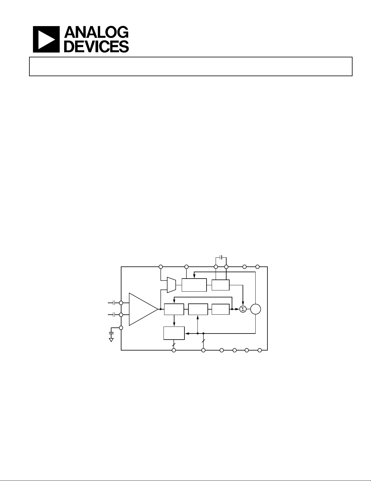
FUNCTIONAL BLOCK DIAGRAM
REFCLKP/N
(OPTIONAL)
LOL
and Data Recovery IC
ADN2815
VCC VEECF1 CF2
PIN
NIN
VREF
Rev. PrA
Information furnished by Analog Devices is believed to be accurate and reliable.
However, no responsibility is assumed by Analog Devices for its use, nor for any
infringements of patents or other rights of third parties that may result from its use.
Specifications subject to change without notice. No license is granted by implication
or otherwise under any patent or patent rights of Analog Devices. Trademarks and
registered trademarks are the property of their respective owners.
BUFFER
PHASE
SHIFTER
DATA
RE-TIMING
2
DATAOUTP/N DRVEE DVCCDRVCC DVEECLKOUTP/N
FREQUENCY
DETECT
PHASE
DETECT
2
Figure 1.
LOOP
FILTER
LOOP
FILTER
One Technology Way, P.O. Box 9106, Norwood, MA 02062-9106, U.S.A.
Tel: 781.329.4700 www.analog.com
Fax: 781.326.8703 © 2004 Analog Devices, Inc. All rights reserved.
VCO
04952-0-001

ADN2815 Preliminary Technical Data
TABLE OF CONTENTS
Specifications..................................................................................... 3
Jitter Specifications....................................................................... 4
Output and Timing Specifications............................................. 5
Absolute Maximum Ratings............................................................ 6
Thermal Characteristics .............................................................. 6
ESD Caution.................................................................................. 6
Timing Characteristics..................................................................... 7
Pin Configuration and Function Descriptions............................. 8
Typical Performance Characteristics ............................................. 9
I2C Interface Timing and Internal Register Description........... 10
Jitter Specifications ......................................................................... 12
Jitter Generation .........................................................................12
Jitter Transfer............................................................................... 12
Jitter Tolerance............................................................................ 12
Theory of Operation ...................................................................... 13
Functional Description.................................................................. 15
Frequency Acquisition............................................................... 15
Input buffer................................................................................. 15
Lock Detector Operation .......................................................... 15
Harmonic Detector.................................................................... 16
Squelch Mode ............................................................................. 16
I2C Interface ................................................................................ 16
Reference Clock (Optional) ...................................................... 17
Applications Information.............................................................. 20
PCB Design Guidelines ............................................................. 20
Coarse Data Rate Readback Look-Up Table............................... 23
Outline Dimensions....................................................................... 25
Ordering Guide .......................................................................... 25
REVISION HISTORY
6/04—Revision PrA: Initial Version
Rev. PrA | Page 2 of 27

Preliminary Technical Data ADN2815
SPECIFICATIONS
TA = T
unless otherwise noted.
Table 1.
Parameter Conditions Min Typ Max Unit
QUANTIZER—DC CHARACTERISTICS
QUANTIZER—AC CHARACTERISTICS
LOSS OF LOCK DETECT (LOL)
GbE 1.0 µs
ACQUISITION TIME
OC-12 2.0 ms
OC-3 3.4 ms
OC-1 9.8 ms
12.3 Mb/s 40.0 ms
DATA RATE READBACK ACCURACY
POWER SUPPLY VOLTAGE 3.0 3.3 3.6 V
POWER SUPPLY CURRENT 90 mA
OPERATING TEMPERATURE RANGE –40 +85 °C
to T
MIN
Input Voltage Range @ PIN or NIN, dc-coupled 1.8 2.8 V
Peak-to-Peak Differential Input PIN – NIN 0.2 2.0 V
Input Common Mode Level DC-coupled 2.3 2.5 2.8 V
Data Rate 12.3 1250 Mb/s
S11 @ 2.5 GHz
Input Resistance Differential 100
Input Capacitance 0.65 pF
VCO Frequency Error for LOL Assert With respect to nominal 1000 ppm
VCO Frequency Error for LOL De-Assert With respect to nominal 250 ppm
LOL Response Time 12.3 Mb/s 4 ms
OC-12 1.0 µs
Lock to Data Mode 1GbE 1.5 ms
Optional Lock to REFCLK Mode 10.0 ms
Coarse Readback (See Table 13) 10 %
Fine Readback In addition to REFCLK accuracy
Data rate < 20 Mb/s 200 ppm
Data rate > 20 Mb/s 100 ppm
, VCC = V
MAX
MIN
to V
, VEE = 0 V, CF = 0.47 µF, SLICEP = SLICEN = VEE, Input Data Pattern: PRBS 223 − 1,
MAX
−15
Ω
dB
Rev. PrA | Page 3 of 27

ADN2815 Preliminary Technical Data
JITTER SPECIFICATIONS
TA = T
unless otherwise noted.
Table 2.
Parameter Conditions Min Typ Max Unit
PHASE-LOCKED LOOP CHARACTERISTICS
30 Hz1 100 UI p-p
300 Hz1 44 UI p-p
25 kHz 2.5 UI p-p
250 kHz1 1.0 UI p-p
OC-3, 223 − 1 PRBS
30 Hz1 50 UI p-p
300 Hz1 24 UI p-p
6500 Hz 3.5 UI p-p
65 kHz 1.0 UI p-p
1
Jitter tolerance of the ADN2815 at these jitter frequencies is better than what the test equipment is able to measure.
MIN
to T
, VCC = V
MAX
MIN
to V
, VEE = 0 V, CF = 0.47 uF, SLICEP = SLICEN = VEE, Input Data Pattern: PRBS 223 − 1,
MAX
Jitter Transfer BW OC-12 71 108 kHz
OC-3 23 35 kHz
Jitter Peaking OC-12 0 0.03 dB
OC-3 0 0.03 dB
Jitter Generation OC-12, 12 kHz to 5 MHz 0.001 0.002 UI rms
0.01 0.019 UI p-p
OC-3, 12 kHz to 1.3 MHz 0.001 0.002 UI rms
0.01 0.011 UI p-p
Jitter Tolerance 1GbE, IEEE802.3
637kHz 0.749 UI p-p
OC-12, 223 − 1 PRBS
Rev. PrA | Page 4 of 27

Preliminary Technical Data ADN2815
OUTPUT AND TIMING SPECIFICATIONS
Table 3.
Parameter Conditions Min Typ Max Unit
LVDS OUPUT CHARACTERISTICS
(CLKOUTP/N, DATAOUTP/N)
Single-Ended Output Swing VSE (see Figure 3) 250 400 mV
Differential Output Swing V
Output Offset Voltage 1125 1200 1275 mV
Output Impedance Differential 100
LVDS Ouputs Timing
Rise Time 20% to 80% TBD ps
Fall Time 80% to 20% TBD ps
Setup Time TS (see Figure 2), GbE 400 ps
Hold Time TH (see Figure 2), GbE 400 ps
I2C INTERFACE DC CHARACTERISTICS LVCMOS
Input High Voltage VIH 0.7 VCC V
Input Low Voltage VIL 0.3 VCC V
Input Current VIN = 0.1 VCC or VIN = 0.9 VCC −10.0 +10.0 µA
Output Low Voltage VOL, I
I2C INTERFACE TIMING (See Figure 9)
SCK Clock Frequency 400 kHz
SCK Pulse Width High t
SCK Pulse Width Low t
Start Condition Hold Time t
Start Condition Setup Time t
Data Setup Time t
Data Hold Time t
SCK/SDA Rise/Fall Time TR/TF 20 + 0.1 Cb
Stop Condition Setup Time t
Bus Free Time between a Stop and a Start t
REFCLK CHARACTERISTICS Optional lock to REFCLK mode
Input Voltage Range @ REFCLKP or REFCLKN
V
V
Minimum Differential Input Drive 100 mV p-p
Reference Frequency 12.3 200 MHz
Required Accuracy 100 ppm
LVTTL DC INPUT CHARACTERISTICS
Input High Voltage VIH 2.0 V
Input Low Voltage VIL 0.8 V
Input High Current IIH, VIN = 2.4 V 5 µA
Input Low Current IIL, VIN = 0.4 V −5 µA
LVTTL DC OUTPUT CHARACTERISTICS
Output High Voltage VOH, IOH = −2.0 mA 2.4 V
Output Low Voltage VOL, IOL = 2.0 mA 0.4 V
1
Cb = total capacitance of one bus line in pF. If mixed with Hs-mode devices, faster fall-times are allowed.
(see Figure 3) 500 800 mV
DIFF
Ω
= 3.0 mA 0.4 V
OL
600 ns
HIGH
1300 ns
LOW
600 ns
HD;STA
600 ns
SU;STA
100 ns
SU;DAT
300 ns
HD;DAT
600 ns
SU;STO
1300 ns
BUF
0 V
IL
VCC V
IH
1
300 ns
Rev. PrA | Page 5 of 27

ADN2815 Preliminary Technical Data
ABSOLUTE MAXIMUM RATINGS
TA = T
µF, SLICEP = SLICEN = VEE, unless otherwise noted.
Table 4.
Parameter Rating
Supply Voltage (VCC) 4.2 V
Minimum Input Voltage (All Inputs) VEE − 0.4 V
Maximum Input Voltage (All Inputs) VCC + 0.4 V
Maximum Junction Temperature 125°C
Storage Temperature −65°C to +150°C
Lead Temperature (Soldering 10 s) 300°C
ESD CAUTION
ESD (electrostatic discharge) sensitive device. Electrostatic charges as high as 4000 V readily accumulate on
the human body and test equipment and can discharge without detection. Although this product features
proprietary ESD protection circuitry, permanent damage may occur on devices subjected to high energy
electrostatic discharges. Therefore, proper ESD precautions are recommended to avoid performance
degradation or loss of functionality.
MIN
to T
, VCC = V
MAX
MIN
to V
, VEE = 0 V, CF = 0.47
MAX
Stress above those listed under Absolute Maximum Ratings may
cause permanent damage to the device. This is a stress rating
only and functional operation of the device at these or any other
conditions above those indicated in the operational sections of
this specification is not implied. Exposure to absolute
maximum rating conditions for extended periods may affect
device reliability.
THERMAL CHARACTERISTICS
Thermal Resistance
32-LFCSP, 4-layer board with exposed paddle soldered to VEE
= 28°C/W.
θ
JA
Rev. PrA | Page 6 of 27

Preliminary Technical Data ADN2815
TIMING CHARACTERISTICS
CLKOUTP
T
T
S
H
DATAOUTP/N
04952-0-002
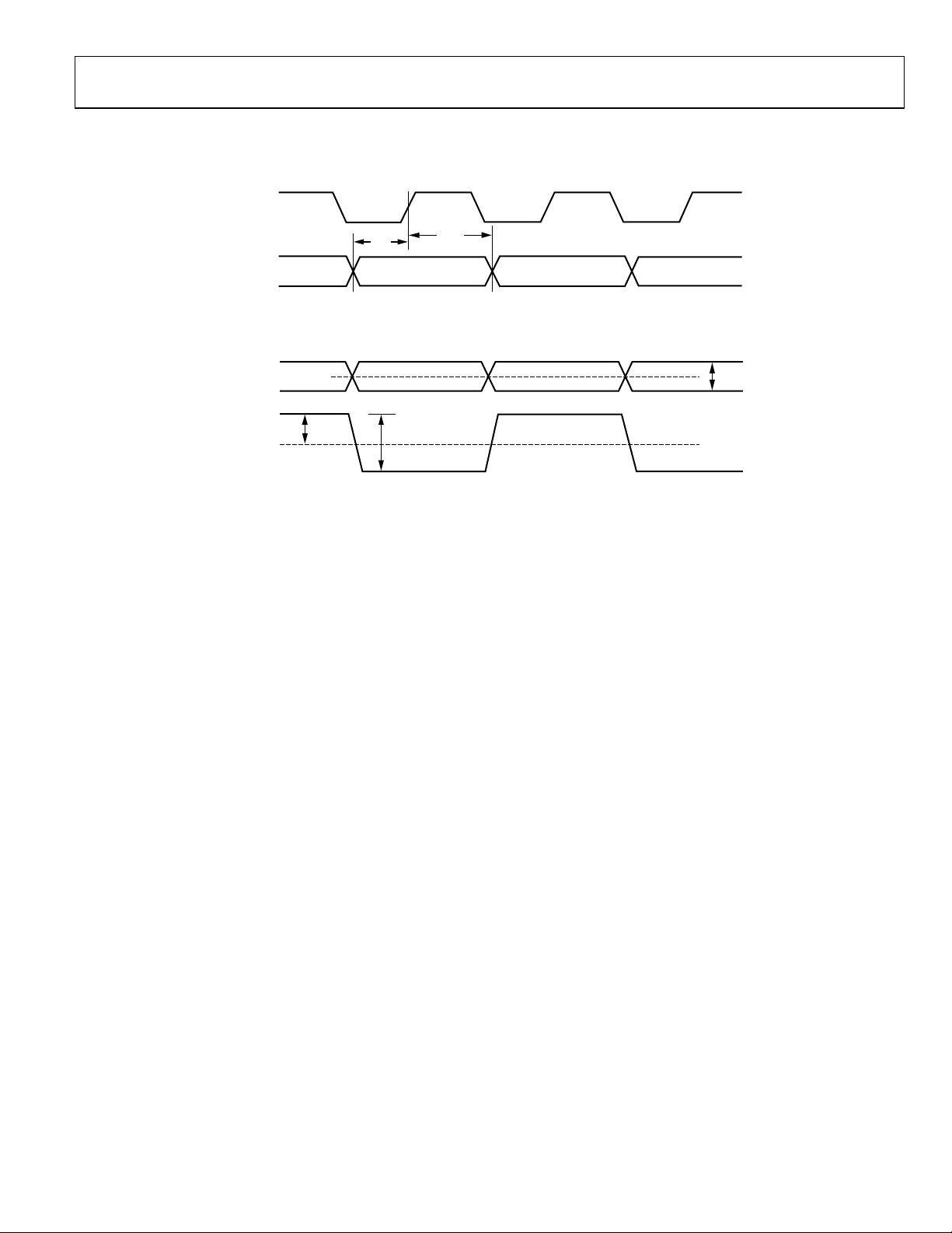
Figure 2. Output Timing
OUTP
OUTN
OUTP–OUTN
V
CML
V
0V
SE
V
DIFF
V
SE
04952-0-003
Figure 3. Single-Ended vs. Differential Output Specifications
Rev. PrA | Page 7 of 27

ADN2815 Preliminary Technical Data
*
PIN CONFIGURATION AND FUNCTION DESCRIPTIONS
32 TEST2
31 VCC
30 VEE
29 DATAOUTP
28 DATAOUTN
27 SQUELCH
26 CLKOUTP
25 CLKOUTN
TEST1 1
VCC 2
VREF 3
NIN 4
PIN 5
NC 6
NC 7
VEE 8
THERE IS AN EXPOSED PAD ON THE BOTTOM OF
THE PACKAGE THAT MUST BE CONNECTED TO GND.
PIN 1
INDICATOR
ADN2815*
TOP VIEW
(Not to Scale)
NC 9
VCC 12
REFCLKP 10
REFCLKN 11
CF2 14
VEE 13
CF1 15
LOL 16
24 VCC
23 VEE
22 NC
21 SDA
20 SCK
19 SADDR5
18 VCC
17 VEE
04952-0-004
Figure 4. Pin Configuration
Table 5. Pin Function Descriptions
Pin No. Mnemonic Type1 Description
1 TEST1 Connect to VCC.
2 VCC P Power for Limamp, LOS.
3 VREF AO Internal VREF Voltage. Decouple to GND with a 0.1 µF capacitor.
4 NIN AI Differential Data Input. CML.
5 PIN AI Differential Data Input. CML.
6 ,7 NC No Connect
8 VEE P GND for Limamp, LOS.
9 NC No Connect
10 REFCLKP DI Differential REFCLK Input. 12.3 MHz to 200 MHz.
11 REFCLKN DI Differential REFCLK Input. 12.3 MHz to 200 MHz.
12 VCC P VCO Power.
13 VEE P VCO GND.
14 CF2 AO Frequency Loop Capacitor.
15 CF1 AO Frequency Loop Capacitor.
16 LOL DO Loss of Lock Indicator. LVTTL active high.
17 VEE P FLL Detector GND.
18 VCC P FLL Detector Power.
19 SADDR5 DI Slave Address Bit 5.
20 SCK DI I
21 SDA DI I
22 NC No Connect
23 VEE P Output Buffer, I
24 VCC P Output Buffer, I
25 CLKOUTN DO Differential Recovered Clock Output. LVDS.
26 CLKOUTP DO Differential Recovered Clock Output. LVDS.
27 SQUELCH DI Disable Clock and Data Outputs. Active high. LVTLL.
28 DATAOUTN DO Differential Recovered Data Output. LVDS.
29 DATAOUTP DO Differential Recovered Data Output. LVDS.
30 VEE P Phase Detector, Phase Shifter GND.
31 VCC P Phase Detector, Phase Shifter Power.
32 TEST2 Connect to VCC.
Exposed Pad Pad P Connect to GND
1
Type: P = power, AI = analog input, AO = analog output, DI = digital input, DO = digital output.
2
C Clock Input.
2
C Data Input.
2
C GND.
2
C Power.
Rev. PrA | Page 8 of 27

Preliminary Technical Data ADN2815
TYPICAL PERFORMANCE CHARACTERISTICS
Rev. PrA | Page 9 of 27
 Loading...