Information furnished by Analog Devices is believed to be accurate and
Analog Devices for its
use; nor for any infringements of patents or other rights of third parties which
may result from its use. No license is granted by implication or otherwise
Multi -
Rate to 2.7Gb p s Clock and Data
Recovery IC with Limi tin g Amp li fi er
CF
Loss of lock
a
Pr eli m i n ary Tech ni c al Data ADN2809
FEATURES
Meets SONET Requ i r ement s for Jitt er Transf er /
Generatio n / Tolerance
Quantizer Sensitiv i ty: 6 mV typi cal
• Adju st able Slice Level: +/- 100 mV
• 1.9GHz minimum Bandwi dt h
Loss of Sign al Detect Range: 4mV to 17mV
Single Reference Clock Frequenc y fo r all rates
Inc l udin g 15/14 (7%) Wrapp er Rate
• Cho ice of 19.44, 38.88, 77.76 or
155.52MHz
LVPECL / LVDS / LVCMOS / LVTTL compati ble
inp u t s (LVPECL / L VDS only at 155.52 MHz)
19.44MHz Cryst al Osci ll ato r fo r Mod u le apps
Loss of Lock indicator
Loop b ack mo d e for High Speed Test Data
Output Squelch & Cloc k Recovery Func tio n s
Single Suppl y Operatio n: 3.3 Volts (+
Low Power: 780 mW Typical
Patented Clock Recovery Archit ectu re
7 x 7 mm 48 pin L FCSP
APPLICATIONS
SONET OC-3/12/48, SDH STM-1/4/16, and all
asso c i ated FEC rates
WDM transpon ders
SONET/SDH regenerato rs and test equi p m ent
Backplane application s
10%)
PRODUCT DESCRIP TI O N
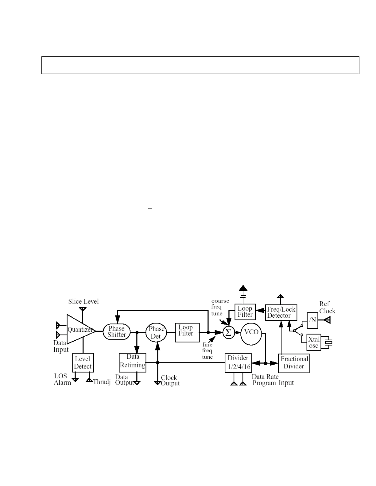
The ADN2809 provides the receiver functions of Quantization,
Signal Level Detect and Clock and Data Recovery at rates of
OC-3, OC-12, Gigabit Ethernet, OC-48 and all FEC rates. All
SONET jitter requirements are met, including: Jitter Transfer;
Jitter Generation; and Jitter Tolerance. All specifications are
quoted for -40 to 85C ambient temperature unless otherwise
noted.
The device is intended for WDM system applications and can be
used with either an external reference clock or an on-chip
oscillator crystal. Both native rates and 15/14 rate digital
‘wrappers’ rates are supported by the ADN2809, without any
change of reference clock required.
This device together with a PIN diode and a TIA preamplifier
can implement a highly integrated, low cost, low power fiber
optic receiver.
The receiver front end Signal Detect circuit indicates when the
input signal level has fallen below a user adjustable threshold.
The ADN2809 is available in a compact 48 pin chip scale
package.
REV. PrB Sept 2001
reliable. However, no responsibility is assumed by
under any patent or patent rights of Analog Devices.
Fun ctional Block Diagram
One Technolog y Way, P.O. Box 9106,
Tel: 781/329-4700 www.analog.com
Fax: 781/326-8703 ©Analog Devi c es, Inc., 2001
Norwo o d, MA 02062-9106 U.S.A.

ADN2809
Para meter
JITTER TOLERANCE TRACKING BANDWIDTH
ADN2809 ELECTRICAL CHARACTERISTICS at T
QUANTIZE R–DC CHARACTERI STICS
Input Voltage Range
Input Common Mode Voltage
Input Peak-to-Peak Differential Voltage
Input Sensitivity, V
Input Overdrive, V
(Peak-to-Peak Differential)
SENSE
OD
Input Maximum Offset Voltage
Input Current
Input RMS Noise
QUANTIZE R-AC CHARACTERI STICS
Upper –3 dB Bandwidth
Small Signal Gain
S11 Maximum @ 2.5GHz, Figure 7
Input Resistance
Input Capacitance
Pulse Width Distortion
QUANTIZ E R SLIC E ADJUSTMENT
Gain (Threshold/Vin)
Control Voltage Range
Control Voltage Range
Slice Threshold Offset
LEVEL DETECT
Level Detect Range (See Figure 4)
Response Time
Hysterises (Electrical), AC Coupled Signal
SDOUT output Logic High
SDOUT output Logic Low
Level Detect Output is a logic “1” LVCMOS
Compatible with no signal present.
POWER SUPPLY VOLTAGE POWER SUPPLY CURRENT PHASE-LOCKED LOOP CHARACTERISTICS
JITTER TRANSFER BANDWIDTH
(See Figure 5 and Table 1)
(See Figure 5 and Table 1)
JITTER TOLERANCE (OC-48)
to T
, VCC=V
to V
A=TMIN
MAX
, VEE=0V, CF=4.7µF, 20 ohm ESR for xo unless otherwise noted
MIN
MAX
Conditions Min Typ Max Units
Single Ended, DC Coupled @ PINor N
“
PINor N
@
AC Coupled I/P
IN
PIN- NIN, Figure 2, BER= <1 x 10
Figure 3, BER = <1 X 10
1
-10
-10
SliceP, SliceN = VCC
-10
1 X 10
BER = <
Differential
Single-Ended
Vin = SliceP-SliceN
SliceP-SliceN
SliceP or SliceN
Full input range
= 0Ω
R
THRESH
R
= 10kΩ
THRESH
R
= 200kΩ
THRESH
DC Coupled
= 0Ω
R
THRESH
R
= 10kΩ
THRESH
R
= 200kΩ
THRESH
Load = +2mA (
Load = -2mA (
to V
V
MIN
to V
V
MIN
NOTE: SONET SPECS APPEAR IN
BOLD
ADN2812 Sources I)
ADN2812 Sinks I)
MAX
MAX
OC-48
Gigabit Ethernet
OC-12
OC-3
OC-48
Gigabit Ethernet
OC-12
OC-3
600 Hz
6 KHz
100 MHz
1 MHz
IN
0
0.4
1.2
1.2
2.4
10
5
6
3
0.5
10
244
µVrms
1.9
54
-15
50
0.65
10
0.131
-0.8
1.3
-1.0
2
6
15
0.1
2.7
3
8.8
17
3
5
5
5
3
0.2
0.134
0.8
VCC
1.0
4
12
21
5
7
7
7
0.4
3.0 3.6 V
140 236 380 mA
1.0
0.5
0.25
0.065
370
185
93
23
4.8
4.8
4.8
4.8
80
>20
5.5
>0.6
2
2
2000
1000
500
130
MHz
MHz
MHz
MHz
UIp-p
UIp-p
UIp-p
UIp-p
V
V
V
mV
mV
mV
µA
GHz
dB
dB
Ω
pF
ps
V/V
V
V
mV
mV
mV
mV
µs
dB
dB
dB
V
V
KHz
KHz
KHz
KHz
JITTER GENERATION
(12kHz to 20MHz)
(12kHz to 10MHz)
(12kHz to 5MHz)
(12kHz to 1.3MHz)
OC-48
Gigabit Ethernet
OC-12
OC-3
REV. PrB Oct. .2001 - 2 -
0.003
0.03
0.003
0.03
0.003
0.03
0.003
0.03
0.01
0.1
0.01
0.1
0.01
0.1
0.01
0.1
UI rms
UIp-p
UI rms
UIp-p
UI rms
UIp-p
UI rms
UIp-p

Para meter
JITTER PEAKING MAXIMUM
ADN2809 ELECTRICAL CHARACTERISTICS at T
CML OUTPUT FORMAT
Single-Ended Output Voltage Swing V
Differential Output Voltage Swing V
Rise Time (t
Fall Time (t
)
R
)
F
DIFF
ADN2809
to T
, VCC=V
to V
A=TMIN
MAX
Conditions Min Typ Max Units
OC-48
Gigabit Ethernet
OC-12
OC-3
SE
See Figure 2 and Figure 6
See Figure 2 and Figure 6
20% - 80%
80% - 20%
, VEE=0V, CF=4.7µF, 20 ohm ESR for xo unless otherwise noted
MIN
MAX
0.1
0.1
0.1
0.1
300
600
430
860
550
1100
150
150
dB
dB
dB
dB
mV
mV
pS
pS
Output High Voltage V
Output Low Voltage V
OH
OL
Data Setup Time T
(Figure 1)
S
Data Hold Time T
(Figure 1)
H
TEST DATA DC CHARACTERI STI CS
Input Voltage Swing V
(Figure 2)
SE
Input Voltage Range
LVTTL DC CHARACTERISTICS
Output High Voltage
V
OH
Output Low Voltage
V
OL
Input High Voltage
V
IH
Input Low Voltage
V
IL
Input High Current
I
IH
Input Low Current
I
IL
REFCL K DC CHARACTE RISTICS
Input Voltage Swing V
(Figure 2)
SE
Input Voltage Range
Note: (1) Recommended for Optimum Sensitivity.
Note: (2) Equipment Limitation.
Figure 6
Figure 6
OC48
Gigabit Ethernet
OC12
OC3
OC48
Gigabit Ethernet
OC12
OC3
Single-Ended
Single-Ended
= -100uA (ADN2809 Sources I)
I
OH
= 1.0mA (ADN2809 Sinks I)
I
OL
Vin = +2.4 V @ +25C
Vin = +0.5 V @ +25C
Single-Ended
Single-Ended
VCC-0.55
150
350
750
3150
150
350
750
3150
0.06
2.3
2.4
2.0
-500
0.032
0
VCC
VCC-0.32
0.8
VCC+0.4
0.5
0.8
50
VCC
VCC
V
V
pS
pS
pS
pS
pS
pS
pS
pS
V
V
V
V
V
V
µA
µA
V
V
ABSOL UTE M AXIMUM RATINGS
Supply Voltage.............................................................. ...+8 V
Input Voltage (pin x or pin xto Vcc).... ........................... .TBD
Maximum Junction Temperature..............................165 deg C
Storage Temperature Range.............. -65 deg C to +150 deg C
Lead Temperature (Soldering 10 sec).. ....................300 deg C
ESD Rating (human body model)....... ........................... ..TBD
Stress above those listed under "Absolute Maximum Ratings" may cause permanent damage
to the device. This is a stress rating only and functional operation of the device at these or any
other conditions above those i ndicated in the operational sections of this s pecification is not
implied. Exposure to absolute maximum rating conditions for extended periods may affect
device reliability.
REV. PrB Oct. .2001 - 3 -
ORDERI NG GUIDE
MODEL TEMP
RANGE
ADN2809XCP -40/+85oC LFCSP-16 CP-16
ADN2809XCP-RL -40/+85oC
Package
Descript-ion
LFCSP-16
2500 Pieces
Option
CP-16

ADN2809
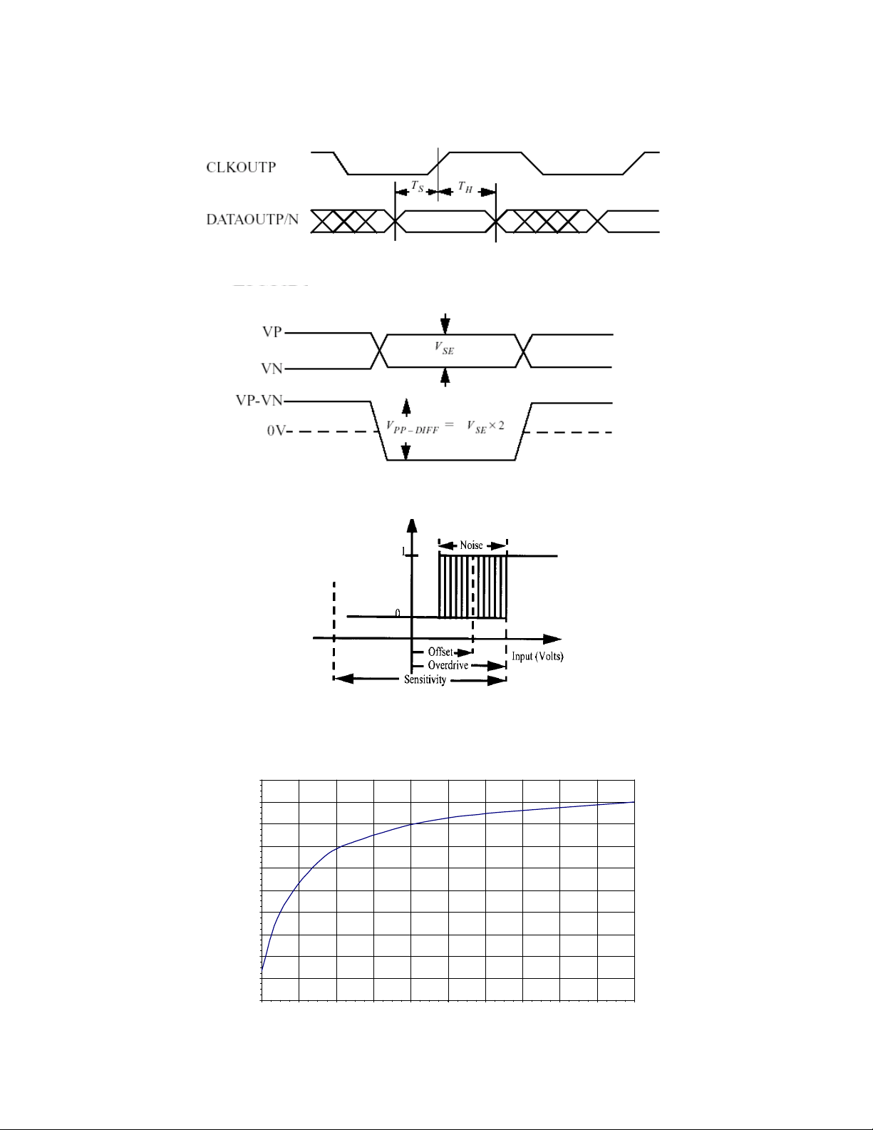
Figure 2. Signal Level Definition
OC-48 2^ 23 LOS Curv e
RThresh
LOS Trip Voltag e (mV)
Figure 1. Output Timing definitions
REV. PrB Oct. .2001 - 4 -
Figure 3. Quantizer Signal Definitions
20.0
18.0
16.0
14.0
12.0
10.0
8.0
6.0
4.0
2.0
0.0
0 20000 40000 60000 80000 100000 120000 140000 160000 180000 2 00 000
Figure 4. LOS Comparator Trip Point Programming
 Loading...