

www.BDTIC.com/ADI
1.25 Gbps Clock and Data Recovery IC
FEATURES
Locks to 1.25 Gbps NRZ serial data input
Patented clock recovery architecture
No reference clock required
Loss-of-lock indicator
2
I
C interface to access optional features
Single-supply operation: 3.3 V
Low power: 390 mW typical
5 mm × 5 mm 32-lead LFCSP, Pb free
APPLICATIONS
GbE line card
GENERAL DESCRIPTION
The ADN2805 provides the receiver functions of quantization
and clock and data recovery for 1.25 Gbps. The ADN2805
automatically locks to all data rates without the need for an
external reference clock or programming. All SONET jitter
requirements are met, including jitter transfer, jitter generation,
and jitter tolerance.
All specifications are specified for −40°C to +85°C ambient
temperature, unless otherwise noted. The ADN2805 is available
in a compact 5 mm × 5 mm 32-lead LFCSP.
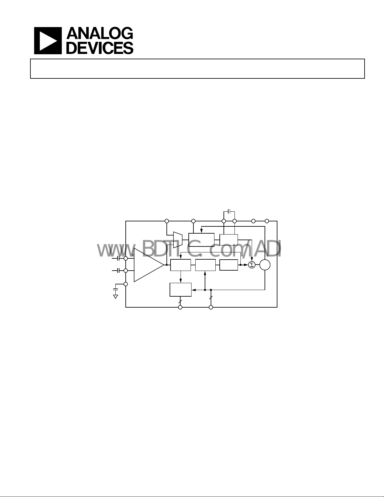
FUNCTIONAL BLOCK DIAGRAM
REFCLKP/REF CLKN
(OPTIO NAL)
LOL
FREQUENCY
DETECT
LOOP
FILTER
ADN2805
VCC VEECF1 CF2
PIN
NIN
VREF
BUFFER
PHASE
SHIFTER
DATA
RE-TIMING
2
DATAOUTP/
DATAOUTN
PHASE
DETECT
CLKOUTP/
CLKOUT N
Figure 1.
LOOP
FILTER
2
VCO
ADN2805
07121-001
Rev. 0
Information furnished by Analog Devices is believed to be accurate and reliable. However, no
responsibility is assumed by Analog Devices for its use, nor for any infringements of patents or other
rights of third parties that may result from its use. Specifications subject to change without notice. No
license is granted by implication or otherwise under any patent or patent rights of Analog Devices.
Trademarks and registered trademarks are the property of their respective owners.
One Technology Way, P.O. Box 9106, Norwood, MA 02062-9106, U.S.A.
Tel: 781.329.4700 www.analog.com
Fax: 781.461.3113 ©2008 Analog Devices, Inc. All rights reserved.

ADN2805
www.BDTIC.com/ADI
TABLE OF CONTENTS
Features .............................................................................................. 1
Applications ....................................................................................... 1
General Description ......................................................................... 1
Functional Block Diagram .............................................................. 1
Revision History ............................................................................... 2
Specifications ..................................................................................... 3
Jitter Specifications ....................................................................... 3
Output and Timing Specifications ............................................. 4
Absolute Maximum Ratings ............................................................ 6
Thermal Characteristics .............................................................. 6
ESD Caution .................................................................................. 6
Pin Configuration and Function Descriptions ............................. 7
I2C Interface Timing and Internal Register Description ............. 8
Theory of Operation ...................................................................... 10
Functional Description .................................................................. 12
Frequency Acquisition ............................................................... 12
Input Buffer ................................................................................. 12
Lock Detector Operation .......................................................... 12
SQUELCH Mode ........................................................................ 13
System Reset ................................................................................ 13
I2C Interface ................................................................................ 13
Applications Information .............................................................. 14
PCB Design Guidelines ............................................................. 14
Outline Dimensions ....................................................................... 16
Ordering Guide .......................................................................... 16
REVISION HISTORY
1/08—Revision 0: Initial Version
Rev. 0 | Page 2 of 16
ADN2805
www.BDTIC.com/ADI
SPECIFICATIONS
TA = T
unless otherwise noted.
Table 1.
Parameter Conditions Min Typ Max Unit
QUANTIZER—DC CHARACTERISTICS
QUANTIZER—AC CHARACTERISTICS
LOSS-OF-LOCK (LOL) DETECT
ACQUISITION TIME
DATA RATE READBACK ACCURACY
POWER SUPPLY
OPERATING TEMPERATURE RANGE −40 +85 °C
to T
MIN
Input Voltage Range @ PIN or NIN, dc-coupled 1.8 2.8 V
Peak-to-Peak Differential Input PIN − NIN 0.2 2.0 V
Input Common-Mode Level DC-coupled 2.3 2.5 2.8 V
Data Rate 1250 Mbps
S11 @ 2.5 GHz −15 dB
Input Resistance Differential 100 Ω
Input Capacitance 0.65 pF
VCO Frequency Error for LOL Assert With respect to nominal 1000 ppm
VCO Frequency Error for LOL Deassert With respect to nominal 250 ppm
LOL Response Time 200 μs
Lock-to-Data Mode GbE 1.5 ms
Optional Lock to REFCLK Mode 20.0 ms
Fine Readback In addition to REFCLK accuracy 100 ppm
Power Supply Voltage 3.0 3.3 3.6 V
Power Supply Current Locked to 1.25 Gbps 118 131 mA
, VCC = V
MAX
MIN
to V
, VEE = 0 V, CF = 0.47 μF, SLICEP = SLICEN = VEE, input data pattern: PRBS 223 − 1,
MAX
JITTER SPECIFICATIONS
TA = T
unless otherwise noted.
Table 2.
Parameter Conditions Min Typ Max Unit
PHASE-LOCKED LOOP CHARACTERISTICS
to T
MIN
Jitter Peaking 0 0.03 dB
Jitter Generation 0.001 0.003 UI rms
0.02 0.04 UI p-p
Jitter Tolerance GbE, IEEE 802.3, 637 kHz 0.749 UI p-p
, VCC = V
MAX
MIN
to V
, VEE = 0 V, CF = 0.47 μF, SLICEP = SLICEN = VEE, input data pattern: PRBS 223 − 1,
MAX
Rev. 0 | Page 3 of 16
ADN2805
www.BDTIC.com/ADI
OUTPUT AND TIMING SPECIFICATIONS
Table 3.
Parameter Conditions Min Typ Max Unit
LVDS OUTPUT CHARACTERISTICS
CLKOUTP/CLKOUTN, DATAOUTP/DATAOUTN
Differential Output Swing VOD (see Figure 3) 240 300 400 mV
Output Offset Voltage VOS (see Figure 3) 1125 1200 1275 mV
Output Impedance Differential 100 Ω
LVDS Outputs Timing
Rise Time 20% to 80% 115 220 ps
Fall Time 80% to 20% 115 220 ps
Setup Time TS (see Figure 2), GbE 360 400 440 ps
Hold Time TH (see Figure 2), GbE 360 400 440 ps
I2C® INTERFACE DC CHARACTERISTICS LVCMOS
Input High Voltage VIH 0.7 VCC V
Input Low Voltage VIL 0.3 VCC V
Input Current VIN = 0.1 VCC or VIN = 0.9 VCC −10.0 +10.0 μA
Output Low Voltage VOL, I
I2C INTERFACE TIMING See Figure 10
SCK Clock Frequency 400 kHz
SCK Pulse Width High t
SCK Pulse Width Low t
Start Condition Hold Time t
Start Condition Setup Time t
Data Setup Time t
Data Hold Time t
SCK/SDA Rise/Fall Time tR/tF 20 + 0.1 Cb
Stop Condition Setup Time t
Bus Free Time Between a Stop and a Start t
REFCLK CHARACTERISTICS Optional lock-to-REFCLK mode
Input Voltage Range @ REFCLKP or REFCLKN
Input Low Voltage VIL 0 V
Input High Voltage VIH VCC V
Minimum Differential Input Drive 100 mV p-p
Reference Frequency 10 160 MHz
Required Accuracy 100 ppm
LVTTL DC INPUT CHARACTERISTICS
Input High Voltage VIH 2.0 V
Input Low Voltage VIL 0.8 V
Input High Current IIH, VIN = 2.4 V 5 μA
Input Low Current IIL, VIN = 0.4 V −5 μA
LVTTL DC OUTPUT CHARACTERISTICS
Output High Voltage VOH, IOH = −2.0 mA 2.4 V
Output Low Voltage VOL, IOL = 2.0 mA 0.4 V
1
Cb = total capacitance of one bus line in pF. If mixed with high speed mode devices, faster fall times are allowed.
= 3.0 mA 0.4 V
OL
600 ns
HIGH
1300 ns
LOW
600 ns
HD;STA
600 ns
SU;STA
100 ns
SU;DAT
300 ns
HD;DAT
600 ns
SU;STO
1300 ns
BUF
1
300 ns
Rev. 0 | Page 4 of 16
ADN2805
www.BDTIC.com/ADI
Timing Characteristics
CLKOUT P
T
T
S
DATAOUTP/
DATAOUTN
V
OH
H
Figure 2. Output Timing
DIFFERENTIAL CLKOUTP/N, DATAOUTP/N
07121-002
V
OS
V
OL
|VOD|
7121-003
Figure 3. Differential Output Specifications
5mA
R
LOAD
V
100Ω
5mA
SIMPLIFIED LVDS
OUTPUT STAGE
100Ω
DIFF
07121-004
Figure 4. Differential Output Stage
Rev. 0 | Page 5 of 16

ADN2805
www.BDTIC.com/ADI
ABSOLUTE MAXIMUM RATINGS
TA = T
0.47 μF, SLICEP = SLICEN = VEE, unless otherwise noted.
Table 4.
Parameter Rating
Supply Voltage (VCC) 4.2 V
Minimum Input Voltage (All Inputs) VEE − 0.4 V
Maximum Input Voltage (All Inputs) VCC + 0.4 V
Maximum Junction Temperature 125°C
Storage Temperature Range −65°C to +150°C
Stresses above those listed under Absolute Maximum Ratings
may cause permanent damage to the device. This is a stress
rating only; functional operation of the device at these or any
other conditions above those indicated in the operational
section of this specification is not implied. Exposure to absolute
maximum rating conditions for extended periods may affect
device reliability.
MIN
to T
, VCC = V
MAX
MIN
to V
, VEE = 0 V, CF =
MAX
THERMAL CHARACTERISTICS
Thermal Resistance
4-layer board with exposed paddle soldered to VEE.
Table 5. Thermal Resistance
Package Type θJA Unit
32-Lead LFCSP 28 °C/W
ESD CAUTION
Rev. 0 | Page 6 of 16

ADN2805
www.BDTIC.com/ADI
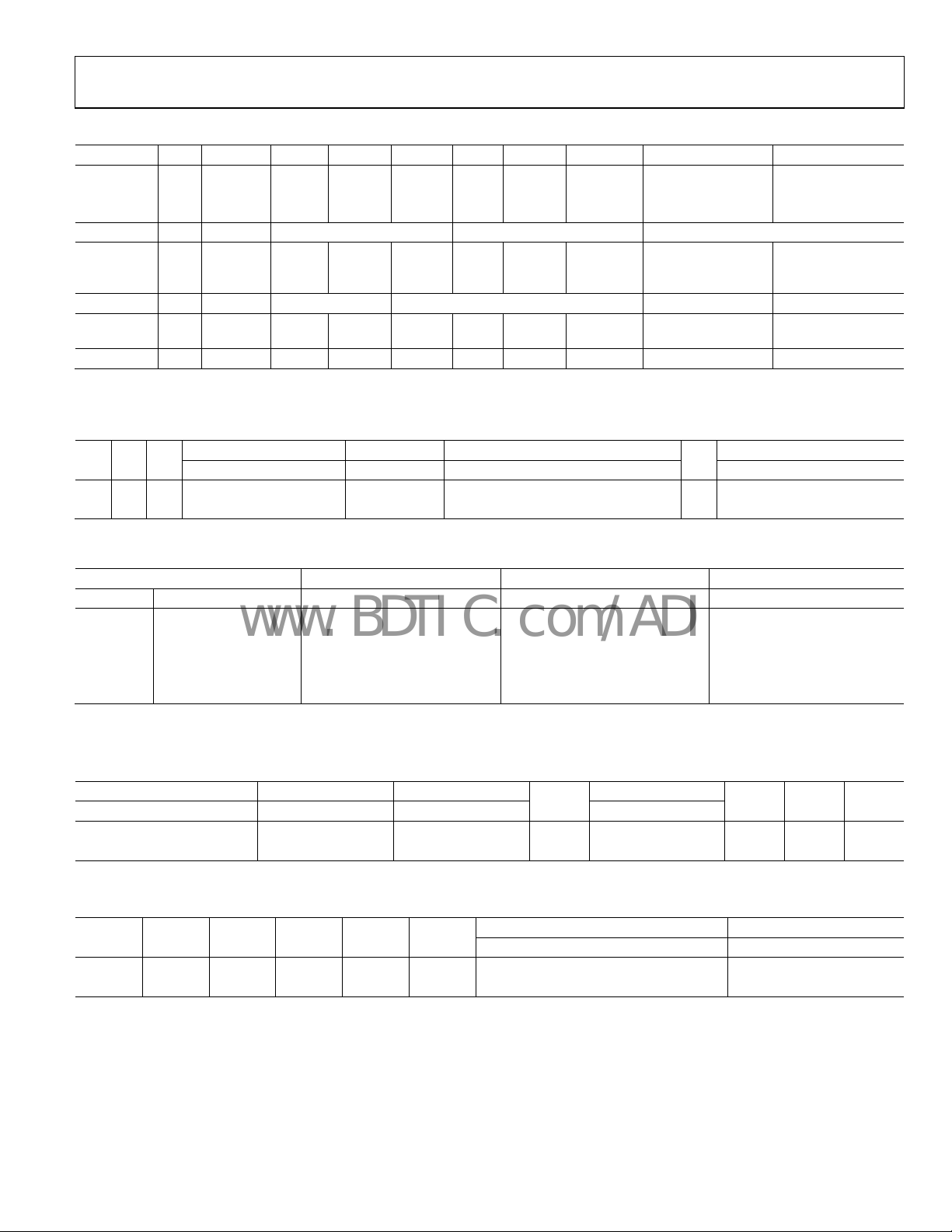
PIN CONFIGURATION AND FUNCTION DESCRIPTIONS
32 TEST2
31 VCC
30 VEE
29 DATAO UTP
28 DATAO UTN
27 SQUELCH
26 CLKOUTP
25 CLKOUTN
TEST1 1
VCC 2
VREF 3
NIN 4
PIN 5
NC 6
NC 7
VEE 8
* THERE IS AN EXPOSED PAD ON THE BOTTOM OF
THE PACKAGE THAT MUST BE CONNE CTED TO GND.
PIN 1
INDIC AT OR
ADN2805*
TOP VIEW
(Not to Scale)
NC 9
VCC 12
REFCLKP 10
REFCLKN 11
VEE 13
CF2 14
CF1 15
LOL 16
24 VCC
23 VEE
22 NC
21 SDA
20 SCK
19 SADDR5
18 VCC
17 VEE
07121-005
Figure 5. Pin Configuration
Table 6. Pin Function Descriptions
Pin No. Mnemonic Type
1
Description
1 TEST1 Connect to VCC.
2 VCC P Power for Limiting Amplifier, LOS.
3 VREF AO Internal VREF Voltage. Decouple to GND with a 0.1 μF capacitor.
4 NIN AI Differential Data Input. CML.
5 PIN AI Differential Data Input. CML.
6, 7, 9, 22 NC No Connect.
8 VEE P GND for Limiting Amplifier, LOS.
10 REFCLKP DI Differential REFCLK Input. 10 MHz to 160 MHz.
11 REFCLKN DI Differential REFCLK Input. 10 MHz to 160 MHz.
12 VCC P VCO Power.
13 VEE P VCO GND.
14 CF2 AO Frequency Loop Capacitor.
15 CF1 AO Frequency Loop Capacitor.
16 LOL DO Loss-of-Lock Indicator. LVTTL active high.
17 VEE P FLL Detector GND.
18 VCC P FLL Detector Power.
19 SADDR5 DI Slave Address Bit 5.
20 SCK DI I2C Clock Input.
21 SDA DI I2C Data Input.
23 VEE P Output Buffer, I2C GND.
24 VCC P Output Buffer, I2C Power.
25 CLKOUTN DO Differential Recovered Clock Output. LVDS.
26 CLKOUTP DO Differential Recovered Clock Output. LVDS.
27 SQUELCH DI Disable Clock and Data Outputs. Active high. LVTTL.
28 DATAOUTN DO Differential Recovered Data Output. LVDS.
29 DATAOUTP DO Differential Recovered Data Output. LVDS.
30 VEE P Phase Detector, Phase Shifter GND.
31 VCC P Phase Detector, Phase Shifter Power.
32 TEST2 Connect to VCC.
Exposed Pad Pad P Connect to GND.
1
Type: P = power, AI = analog input, AO = analog output, DI = digital input, DO = digital output.
Rev. 0 | Page 7 of 16
ADN2805
www.BDTIC.com/ADI
I2C INTERFACE TIMING AND INTERNAL REGISTER DESCRIPTION
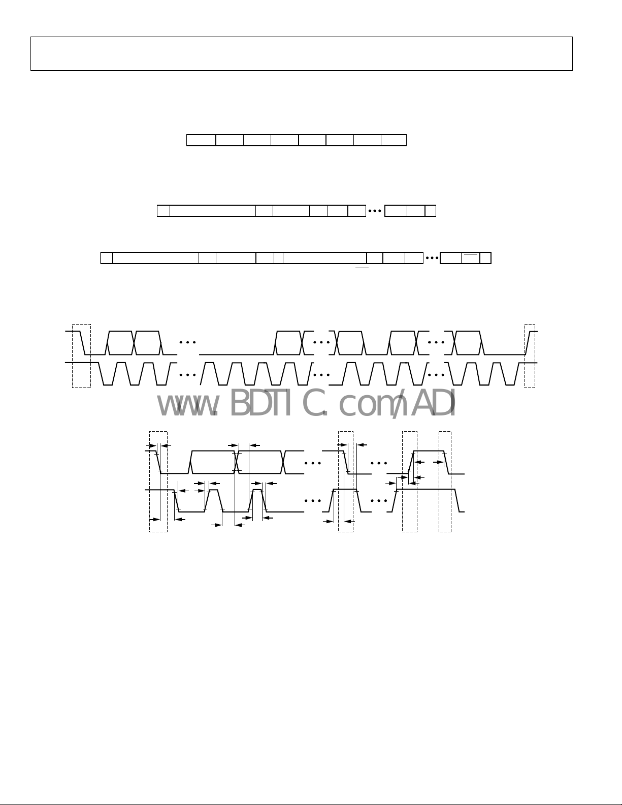
SLAVE ADDRESS [6...0]
1A500000X
MSB = 1 SET BY
PIN 19
Figure 6. Slave Address Configuration
R/W
CTRL.
0 = WR
1 = RD
07121-006
S SLAVE ADDR, LSB = 0 (W R) A(S) A(S) A(S)DATASUB ADDR A(S) PDATA
Figure 7. I
2
C Write Data Transfer
07121-007
S
S = START BIT P = STOP BIT
A(S) = ACKNOWLEDG E BY SLAVE A(M) = ACKNOWLEDGE BY MASTER
SSLAVE ADDR, LSB = 0 (WR) SLAVE ADDR, LSB = 1 (RD)A(S) A(S)SUB ADDR A(S) DATA A(M) DATA PA(M)
A(M) = LACK OF ACKNOWLEDGE BY MASTER
Figure 8. I
2
C Read Data Transfer
7121-008
SDA
SCK
START BIT
S
SLAVE ADDRESS SUB ADDRESS DATA
SLADDR[4... 0]
Figure 9. I
SUB ADDR[6...1] DATA[6...1]
2
C Data Transfer Timing
D0D7A0A7A5A6
STOP BIT
ACKACKWR ACK
P
07121-009
t
F
SDA
t
SCK
SS
LOW
t
HD;STA
t
R
t
HD;DAT
t
SU;DAT
Figure 10. I
t
F
t
HIGH
t
SU;STA
2
C Port Timing Diagram
t
HD;STA
t
SU;STO
t
BUF
t
R
PS
07121-010
Rev. 0 | Page 8 of 16
ADN2805
www.BDTIC.com/ADI
Table 7. Internal Register Map
1, 2
Reg. Name R/W Address D7 D6 D5 D4 D3 D2 D1 D0
FREQ0 R 0x0 MSB LSB
FREQ1 R 0x1 MSB LSB
FREQ2 R 0x2 0 MSB LSB
RATE R 0x3 COARSE_RD[8] MSB Coarse Data Rate Readback COARSE_RD[1]
MISC R 0x4 X X X
Static
LOL
LOL
Status
Data Rate
Measure
X
COARSE_RD[0]
(LSB)
Complete
CTRLA W 0x8 f
CTRLB W 0x9
Range Data Rate/DIV_f
REF
Config
LOL
Reset
MISC[4]
System
Reset
Ratio Measure Data Rate Lock to Reference
REF
0
Reset
0 0 0
MISC[2]
CTRLC W 0x11 0 0 0 0 0 0 Squelch Mode Output Boost
1
All writeable registers default to 0x00.
2
X = don’t care.
Table 8. Miscellaneous Register, MISC1
Static LOL LOL Status Data Rate Measurement Complete Coarse Rate Readback LSB
D7 D6 D5 D4 D3 D2 D1 D0
X X X 0 = waiting for next LOL 0 = locked 0 = measuring data rate X COARSE_RD[0]
1 = static LOL until reset 1 = acquiring 1 = measurement complete
1
X = don’t care.
Table 9. Control Register, CTRLA1
f
Range Data Rate/DIV_f
REF
Ratio Measure Data Rate Lock to Reference
REF
D7 D6 D5 D4 D3 D2 D1 D0
0 0 10 MHz to 20 MHz 0 0 0 0 1 Set to 1 to measure data rate 0 = lock to input data
0 1 20 MHz to 40 MHz 0 0 0 1 2 1 = lock to reference clock
1 0 40 MHz to 80 MHz 0 0 1 0 4
1 1 80 MHz to 160 MHz n 2n
1 0 0 0 256
1
Where DIV_f
is the divided down reference referred to the 10 MHz to 20 MHz band.
REF
Table 10. Control Register, CTRLB
Configure LOL Reset MISC[4] System Reset Reset MISC[2]
D7 D6 D5 D4 D3 D2 D1 D0
0 = LOL pin normal operation
1 = LOL pin is static LOL
Write a 1 followed by
0 to reset MISC[4]
Write a 1 followed by
0 to reset ADN2805
Table 11. Control Register, CTRLC
Squelch Mode Output Boost
D7 D6 D5 D4 D3 D2 D1 D0
Set to 0 Set to 0 Set to 0 Set to 0 Set to 0 Set to 0 0 = SQUELCH DATAOUT and CLKOUT 0 = default output swing
Rev. 0 | Page 9 of 16
Set to 0
Write a 1 followed by
Set to 0 Set to 0 Set to 0
0 to reset MISC[2]
1 = SQUELCH DATAOUT or CLKOUT 1 = boost output swing

ADN2805
G
www.BDTIC.com/ADI
THEORY OF OPERATION
The ADN2805 is a delay- and phase-locked loop circuit for
clock recovery and data retiming from an NRZ encoded data
stream. The phase of the input data signal is tracked by two
separate feedback loops that share a common control voltage. A
high speed delay-locked loop path uses a voltage controlled
phase shifter to track the high frequency components of input
jitter. A separate phase control loop, comprised of the VCO,
tracks the low frequency components of input jitter. The initial
frequency of the VCO is set by yet a third loop, which compares
the VCO frequency with the input data frequency and sets the
coarse tuning voltage. The jitter tracking phase-locked loop
(PLL) controls the VCO by the fine-tuning control.
The delay and phase loops together track the phase of the input
data signal. For example, when the clock lags input data, the
phase detector drives the VCO to a higher frequency and
increases the delay through the phase shifter; both of these
actions serve to reduce the phase error between the clock and
data. The faster clock picks up phase, while simultaneously, the
delayed data loses phase. Because the loop filter is an integrator,
the static phase error is driven to zero.
Another view of the circuit is that the phase shifter implements
the zero required for frequency compensation of a second-order
phase-locked loop, and this zero is placed in the feedback path
and, thus, does not appear in the closed-loop transfer function.
Jitter peaking in a conventional second-order phase-locked loop
is caused by the presence of this zero in the closed-loop transfer
function. Because this circuit has no zero in the closed-loop
transfer, jitter peaking is minimized.
The delay and phase loops together simultaneously provide
wideband jitter accommodation and narrow-band jitter
filtering. The linearized block diagram in
the jitter transfer function, Z(s)/X(s), is second-order low-pass,
providing excellent filtering. Note that the jitter transfer has no
zero, unlike an ordinary second-order phase-locked loop. This
means that the main PLL has virtually zero jitter peaking (see
Figure 12). This makes this circuit ideal for signal regenerator
applications where jitter peaking in a cascade of regenerators
can contribute to hazardous jitter accumulation.
The error transfer, e(s)/X(s), has the same high-pass form as an
ordinary phase-locked loop. This transfer function is free to be
optimized to give excellent wideband jitter accommodation
because the jitter transfer function, Z(s)/X(s), provides the
narrow-band jitter filtering.
Figure 11 shows that
psh
Z(s)
n psh
e(s)
d/sc
JITTER T RANSFER FUNCTI ON
Z(s)
=
X(s)
2
s
TRACKING ERROR T RANSFER FUNCTI ON
e(s)
=
X(s)
2
s
o
d psh
FREQUENCY ( kHz)
o/s
1/n
1
cn
n psh
+
s+ 1
do
o
2
s
d psh
do
s++
c
cn
JITTER PEAKIN
IN ORDINARY PLL
c
ADN2805
Z(s)
X(s)
07121-011
07121-012
X(s)
INPUT
DATA
RECOVERED
CLOCK
d = PHASE DETECTOR GAIN
o = VCO GAIN
c = LOOP INTEGRATOR
psh = PHASE SHIFTER GAIN
n = DIVIDE RATIO
Figure 11. ADN2805 PLL/DLL Architecture
JITTER GAIN (dB)
Figure 12. ADN2805 Jitter Response vs. Conventional PLL
The delay and phase loops contribute to overall jitter accommodation. At low frequencies of input jitter on the data signal,
the integrator in the loop filter provides high gain to track large
jitter amplitudes with small phase error. In this case, the VCO is
frequency modulated and jitter is tracked as in an ordinary
phase-locked loop. The amount of low frequency jitter that can
be tracked is a function of the VCO tuning range. A wider
tuning range gives larger accommodation of low frequency
jitter. The internal loop control voltage remains small for small
phase errors; therefore, the phase shifter remains close to the
center of its range and thus contributes little to the low
frequency jitter accommodation.
At medium jitter frequencies, the gain and tuning range of the
VCO are not large enough to track input jitter. In this case, the
VCO control voltage becomes large and saturates, and the VCO
frequency dwells at either one extreme of its tuning range or at
the other. The size of the VCO tuning range, therefore, has only
a small effect on the jitter accommodation. As such, the delaylocked loop control voltage is larger, and, consequently, the
phase shifter takes on the burden of tracking the input jitter.
The phase shifter range, in UI, can be seen as a broad plateau on
the jitter tolerance curve. The phase shifter has a minimum
range of 2 UI at all data rates.
Rev. 0 | Page 10 of 16

ADN2805
www.BDTIC.com/ADI
The gain of the loop integrator is small for high jitter
frequencies; therefore, larger phase differences are needed to
make the loop control voltage large enough to tune the range of
the phase shifter. Large phase errors at high jitter frequencies
cannot be tolerated. In this region, the gain of the integrator
determines the jitter accommodation. Because the gain of the
loop integrator declines linearly with frequency, jitter accommodation is lower with higher jitter frequency. At the highest
frequencies, the loop gain is very small, and little tuning of the
phase shifter can be expected. In this case, jitter accommodation is
determined by the eye opening of the input data, the static
phase error, and the residual loop jitter generation. The jitter
accommodation is roughly 0.5 UI in this region. The corner
frequency between the declining slope and the flat region is
the closed loop bandwidth of the delay-locked loop, which is
roughly 1.5 MHz at 1.25 Gbps.
Rev. 0 | Page 11 of 16

ADN2805
www.BDTIC.com/ADI
FUNCTIONAL DESCRIPTION
FREQUENCY ACQUISITION
The ADN2805 acquires frequency from the data at 1.25 Gbps.
The lock detector circuit compares the frequency of the VCO
and the frequency of the incoming data. When these frequencies differ by more than 1000 ppm, LOL asserts. This initiates a
frequency acquisition cycle. An on-chip frequency-locked loop
(FLL) forces the frequency of the VCO to be approximately
equal to the frequency of the incoming data. LOL is deasserted
once the VCO frequency is within 250 ppm of the data frequency.
When LOL deasserts, the FLL turns off. The PLL/DLL pulls in
the VCO frequency until the VCO frequency equals the data
frequency.
The frequency loop requires a single external capacitor between
CF1 and CF2, Pin 15 and Pin 14. A 0.47 μF ± 20%, X7R ceramic
chip capacitor with <10 nA leakage current is recommended.
Calculate the leakage current of the capacitor by dividing the
maximum voltage across the 0.47 μF capacitor, ~3 V, by the
insulation resistance of the capacitor. The insulation resistance
of the 0.47 μF capacitor should be greater than 300 MΩ.
INPUT BUFFER
The input buffer has differential inputs (PIN/NIN), which are
internally terminated with 50 Ω to an on-chip voltage reference
(VREF = 2.5 V typically). The minimum differential input level
required to achieve a BER of 10
LOCK DETECTOR OPERATION
The lock detector on the ADN2805 has three modes of
operation: normal mode, REFCLK mode, and static LOL mode.
Normal Mode
In normal mode, the ADN2805 locks onto 1.25 Gbps NRZ data
without the use of a reference clock as an acquisition aid. In this
mode, the lock detector monitors the frequency difference
between the VCO and the input data frequency, and deasserts
the loss-of-lock signal, which appears on Pin 16 (LOL) when
the VCO is within 250 ppm of the data frequency. This enables
the DLL/PLL, which pulls the VCO frequency in the remaining
amount and acquires phase lock. When locked, if the input
frequency error exceeds 1000 ppm (0.1%), the loss-of-lock
signal reasserts and control returns to the frequency loop,
which begins a new frequency acquisition. The LOL pin
remains asserted until the VCO locks onto a valid input data
stream to within 250 ppm frequency error. This hysteresis is
shown in Figure 13.
−10
is 200 mV p-p.
LOL
1
–1000
Figure 13. Transfer Function of LOL
0–250 250 1000
f
VCO
(ppm)
ERROR
07121-013
LOL Detector Operation Using a Reference Clock
In REFCLK mode, a reference clock is used as an acquisition aid
to lock the ADN2805 VCO. Lock-to-reference mode is enabled
by setting CTRLA[0] to 1. The user also needs to write to the
CTRLA[7:6] and CTRLA[5:2] bits to set the reference frequency
range and the divide ratio of the data rate with respect to the
reference frequency. In this mode, the lock detector monitors
the difference in frequency between the divided down VCO
and the divided down reference clock. The loss-of-lock signal,
which appears on Pin 16 (LOL), deasserts when the VCO is
within 250 ppm of the desired frequency. This enables the DLL/
PLL, which pulls the VCO frequency in the remaining amount
with respect to the input data and acquires phase lock. When
locked, if the input frequency error exceeds 1000 ppm (0.1%),
the loss-of-lock signal reasserts and control returns to the frequency loop, which reacquires with respect to the reference
clock. The LOL pin remains asserted until the VCO frequency
is within 250 ppm of the desired frequency. This hysteresis is
shown in Figure 13.
Static LOL Mode
The ADN2805 implements a static LOL feature to indicate
whether a loss-of-lock condition has ever occurred and remains
asserted, even if the ADN2805 regains lock, until the static LOL
bit is manually reset. The I
2
C register bit, MISC[4], is the static
LOL bit. If there is ever an occurrence of a loss-of-lock condition,
this bit internally asserts to Logic high. The MISC[4] bit remains
high even after the ADN2805 has reacquired lock to a new data
rate. This bit can be reset by writing a 1 followed by 0 to I
2
C
Register Bit CTRLB[6]. When reset, the MISC[4] bit remains
deasserted until another loss-of-lock condition occurs.
Writ i ng a 1 t o I
2
C Register Bit CTRLB[7] causes the LOL pin,
Pin 16, to become a static LOL indicator. In this mode, the LOL
pin mirrors the contents of the MISC[4] bit and has the functionality described in the previous paragraph.
The CTRLB[7] bit defaults to 0. In this mode, the LOL pin
operates in the normal operating mode, that is, it asserts only
when the ADN2805 is in acquisition mode and deasserts when
the ADN2805 reacquires lock.
Rev. 0 | Page 12 of 16

ADN2805
www.BDTIC.com/ADI
SQUELCH MODE
Two squelch modes are available with the ADN2805. The
SQUELCH DATAOUT and CLKOUT mode is selected when
CTRLC[1] = 0 (default mode). In this mode, when the SQUELCH
input, Pin 27, is driven to a TTL high state, both the clock and
data outputs are set to the zero state to suppress downstream processing. If the squelch function is not required, tie Pin 27 to VEE.
SQUELCH DATAOUT or CLKOUT mode is selected when
CTRLC[1] is 1. In this mode, when the SQUELCH input is
driven to a high state, the DATAOUTN/DATAOUTP pins
are squelched. When the SQUELCH input is driven to a low
state, the CLKOUT pins are squelched. This feature is especially
useful in repeater applications, where the recovered clock may
not be needed.
SYSTEM RESET
A frequency acquisition can be initiated by writing a 1 followed
by a 0 to the I
frequency acquisition while keeping the ADN2805 in the
operating mode that it was previously programmed to in
Register CTRL[A], Register CTRL[B], and Register CTRL[C].
2
C Register Bit CTRLB[5]. This initiates a new
I2C INTERFACE
The ADN2805 supports a 2-wire, I2C-compatible, serial bus
driving multiple peripherals. Two inputs, serial data (SDA) and
serial clock (SCK), carry information between any devices
connected to the bus. Each slave device is recognized by a
unique address. The ADN2805 has two possible 7-bit slave
addresses for both read and write operations. The MSB of the
7-bit slave address is factory programmed to 1. Bit 5 of the slave
address is set by Pin 19, SADDR5. Slave Address Bits[4:0] are
defaulted to all 0s. The slave address consists of the 7 MSBs of
an 8-bit word. The LSB of the word either sets a read or write
operation (see Figure 6). Logic 1 corresponds to a read
operation whereas Logic 0 corresponds to a write operation.
To control the device on the bus, the following protocol must be
followed. First, the master initiates a data transfer by establishing
a start condition, defined by a high-to-low transition on SDA
while SCK remains high. This indicates that an address/data
stream follows. All peripherals respond to the start condition
and shift the next eight bits (the 7-bit address and the R/
W
bit).
The bits are transferred from MSB to LSB. The peripheral that
recognizes the transmitted address responds by pulling the data
line low during the ninth clock pulse. This is known as an acknowledge bit. All other devices withdraw from the bus at this point
and maintain an idle condition. The idle condition is where the
device monitors the SDA and SCK lines waiting for the start
condition and correct transmitted address. The R/
mines the direction of the data. Logic 0 on the LSB of the first
byte means that the master writes information to the peripheral.
Logic 1 on the LSB of the first byte means that the master reads
information from the peripheral.
The ADN2805 acts as a standard slave device on the bus. The data
on the SDA pin is eight bits long, supporting the 7-bit addresses,
plus the R/
the user-accessible internal registers (see through ).
It, therefore, interprets the first byte as the device address and
the second byte as the starting subaddress. Auto-increment
mode is supported, allowing data to be read from or written to
the starting subaddress and each subsequent address without
manually addressing the subsequent subaddress. A data transfer is always terminated by a stop condition. The user can also
access any unique subaddress register on a one-by-one basis
without updating all registers.
Stop and start conditions can be detected at any stage of the
data transfer. If these conditions assert out of sequence with
normal read and write operations, they cause an immediate
jump to the idle condition. During a given SCK high period,
the user should issue one start condition, one stop condition,
or a single stop condition followed by a single start condition.
If an invalid subaddress is issued by the user, the ADN2805
does not issue an acknowledge and returns to the idle condition. If the user exceeds the highest subaddress while reading
back in auto-increment mode, the highest subaddress register
contents continue to be output until the master device issues a
no-acknowledge. This indicates the end of a read. In a no-acknowledge condition, the SDATA line is not pulled low on the ninth
pulse. See Figure 7 and Figure 8 for sample read and write data
transfers and Figure 9 for a more detailed timing diagram.
W
bit. The ADN2805 has eight subaddresses to enable
Tabl e 7 Tabl e 1 1
W
bit deter-
Rev. 0 | Page 13 of 16

ADN2805
(
=
www.BDTIC.com/ADI
APPLICATIONS INFORMATION
PCB DESIGN GUIDELINES
Proper RF PCB design techniques must be used for optimal
performance.
Power Supply Connections and Ground Planes
Use of one low impedance ground plane is recommended. To
reduce series inductance, solder the VEE pins directly to the
ground plane. If the ground plane is an internal plane and
connections to the ground plane are made through vias, multiple
vias can be used in parallel to reduce the series inductance,
especially on Pin 23, which is the ground return for the output
buffers. Connect the exposed pad to the ground plane using
plugged vias to prevent solder from leaking through the vias
during reflow.
Use of a 22 μF electrolytic capacitor between VCC and VEE is
recommended at the location where the 3.3 V supply enters the
PCB. When using 0.1 μF and 1 nF ceramic chip capacitors,
place them between the IC power supply VCC and VEE, as
close as possible to the ADN2805 VCC pins.
VCC
+
0.1µF22µF 1n F
If connections to the supply and ground are made through vias,
the use of multiple vias in parallel helps to reduce series
inductance, especially on Pin 24, which supplies power to the
high speed CLKOUTP/CLKOUTN and DATAOUTP/
DATAOUTN output buffers. Refer to Figure 14 for the
recommended connections.
By using adjacent power supply and ground planes, excellent
high frequency decoupling can be realized by using close
spacing between the planes. This capacitance is given by
)
pFε88.0 A/dC
PLANE
r
where:
is the dielectric constant of the PCB material.
ε
r
A is the area of the overlap of power and ground planes (cm
2
).
d is the separation between planes (mm).
For FR-4, ε
50Ω TRANSMISSION LINES
= 4.4 mm and 0.25 mm spacing, C ~15 pF/cm2.
r
DATAOUTP
DATAOUTN
CLKOUTP
CLKOUTN
0.1µF
TRANSCEIVER
1nF
0.1µF
OPTICAL
MODULE
50Ω
50Ω
TEST1
VCC
VREF
NIN
PIN
NC
NC
VEE
VCC
0.1µF
CC
V
VEE
TEST2
31
32
1
2
EXPOSED PAD
3
TIED OFF TO
4
VEE PLANE
5
WITH VIAS
6
7
8
9
10
REFCLKP
REFCLKN
NC
1nF
TAOUTP
DATAOUTN
SQUELCH
DA
CLKOUTN
CLKOUTP
29
28
27
26
30
11
VCC
NC
25
VCC
24
VEE
23
NC
22
SDA
21
SCK
20
SADDR5
19
VCC
18
VEE
17
15
13
14
12
CF1
CF2
LOL
VEE
0.47µF ±20%
>300MΩ INSULATI ON RESISTANCE
1nF
16
µC
VCC
0.1µF1nF
2
C CONTROLL ER
I
2
I
C CONTROLL ER
VCC
0.1µF
07121-014
Figure 14. Typical Applications Circuit
Rev. 0 | Page 14 of 16

ADN2805
V
VCC
V
V
www.BDTIC.com/ADI
Transmission Lines
Use of 50 Ω transmission lines is required for all high frequency
input and output signals to minimize reflections: PIN, NIN,
CLKOUTP, CLKOUTN, DATAOUTP, and DATAOUTN (also
REFCLKP and REFCLKN, if a high frequency reference clock is
used, such as 155 MHz). It is also necessary for the PIN/NIN
input traces to be matched in length, and the CLKOUTP/
CLKOUTN and DATAOUTP/DATAOUTN output traces to be
matched in length to avoid skew between the differential traces.
The high speed inputs, PIN and NIN, are internally terminated
with 50 Ω to an internal reference voltage (see Figure 15).
A 0.1 μF is recommended between VREF, Pin 3, and GND to
provide an ac ground for the inputs.
As with any high speed mixed-signal design, take care to keep
all high speed digital traces away from sensitive analog nodes.
CC
ADN2805
C
50Ω
IN
PIN
TIA
50Ω
0.1µF
C
IN
NIN
50Ω
50Ω
VREF
3kΩ
2.5V
07121-015
Figure 15. AC-Coupled Input Configuration
Soldering Guidelines for Lead Frame Chip Scale Package
The lands on the 32-lead LFCSP are rectangular. The printed
circuit board (PCB) pad for these should be 0.1 mm longer than
the package land length and 0.05 mm wider than the package
land width. The land should be centered on the pad. This
ensures that the solder joint size is maximized. The bottom of
the chip scale package has a central exposed pad. The pad on
the PCB should be at least as large as this exposed pad. The user
must connect the exposed pad to VEE using plugged vias so
that solder does not leak through the vias during reflow. This
ensures a solid connection from the exposed pad to VEE.
C
IN
V1
TIA BUFFER
1
V1
V1b
V2
V2b
DIFF
V
= V2 – V2b
DIFF
VTH = ADN2805 QUANTIZE R THRESHOLD
NOTES:
1. DURING DATA PATTERNS WITH HIG H TRANSITI ON DENSITY, DIFFERENTIAL DC VOLTAGE AT V1 AND V2 IS ZERO.
2. WHEN THE OUT PUT OF THE TIA GOES TO CID, V1 AND V1b ARE DRIVEN TO DIF FERENT DC LEVELS. V2 AND V2b DISCHARGE TO THE
VREF LEVEL , WHICH EF FECTIV ELY INTRO DUCES A DIFFERENTI AL DC OFFSET ACROSS THE AC COUPLI NG CAPACITORS.
3. WHEN THE BURST OF DATA STARTS AGAI N, THE DIFFERENTI AL DC OFFSET ACROSS THE AC COUPLI NG CAPACITORS IS APPLIE D TO
THE INPUT LEVELS CAUSING A DC SHIFT IN THE DIFFERENTIAL INPUT. THIS SHIFT IS LARGE ENOUGH SUCH THAT ONE OF THE STATES,
EITHER HIG H OR LOW DEPENDING ON T HE LEVEL S OF V1 AND V1b WHEN T HE TIA WENT TO CID, I S CANCELED OUT. THE QUANTIZ ER
DOES NOT RECO GNIZE THIS AS A VALID STATE.
4. THE DC OFF SET SLO WLY DI SCHARGES UNTI L THE DIFF ERENTIAL INPUT VOLTAGE EXCEEDS THE SENSITI VITY OF THE ADN2805. THE
QUANTIZER CAN RECO GNIZE BOTH HIGH AND LOW STATES AT THIS POINT.
V1b
V2
PIN
50Ω
V
NIN
50Ω
REF
C
IN
V2b
234
Figure 16. Example of Baseline Wander
+
–
ADN2805
CDR
C
OUT
C
OUT
DATAOUTP
DATAOUTN
REF
VTH
07121-016
Rev. 0 | Page 15 of 16

ADN2805
www.BDTIC.com/ADI
OUTLINE DIMENSIONS
PIN 1
INDICATOR
1.00
0.85
0.80
12° MAX
SEATING
PLANE
0.08
0.60 MAX
25
24
EXPOSED
PAD
(BOTTOM VIEW)
17
16
5.00
BSC SQ
TOP
VIEW
0.80 MAX
0.65 TYP
0.30
0.23
0.18
COMPLIANT TO JEDEC STANDARDS MO-220-VHHD-2
4.75
BSC SQ
0.20 REF
0.05 MAX
0.02 NOM
0.60 MAX
0.50
BSC
0.50
0.40
0.30
COPLANARITY
Figure 17. 32-Lead Lead Frame Chip Scale Package [LFCSP_VQ]
5 mm × 5 mm Body, Very Thin Quad
(CP-32-2)
Dimensions shown in millimeters
32
1
8
9
3.50 REF
PIN 1
INDICATOR
3.25
3.10 SQ
2.95
0.25 MIN
ORDERING GUIDE
Model Temperature Range Package Description Package Option
ADN2805ACPZ
ADN2805ACPZ-500RL7
ADN2805ACPZ-RL7
EVAL-ADN2805EBZ
1
Z = RoHS Compliant Part.
Purchase of licensed I
Rights to use these components in an I2C system, provided that the system conforms to the I2C Standard Specification as defined by Philips.
©2008 Analog Devices, Inc. All rights reserved. Trademarks and
registered trademarks are the property of their respective owners.
D07121-0-1/08(0)
1
1
−40°C to +85°C 32-Lead LFCSP_VQ, Tape-Reel, 500 pieces CP-32-2
1
−40°C to +85°C 32-Lead LFCSP_VQ, Tape-Reel, 1,500 pieces CP-32-2
1
Evaluation Board
2
C components of Analog Devices or one of its sublicensed Associated Companies conveys a license for the purchaser under the Philips I2C Patent
−40°C to +85°C 32-Lead LFCSP_VQ CP-32-2
Rev. 0 | Page 16 of 16
 Loading...