

Page 1
622 Mbps Clock and Data Recovery IC
www.BDTIC.com/ADI
FEATURES
Exceeds SONET requirements for jitter transfer/
generation/tolerance
Quantizer sensitivity: 3.3 mV typical
Adjustable slice level: ±95 mV
Patented clock recovery architecture
Loss-of-signal (LOS) detect range: 2.6 mV to 18.4 mV
Independent slice level adjust and LOS detector
No reference clock required
Loss-of-lock indicator
I2C® interface to access optional features
Single-supply operation: 3.3 V
Low power: 423 mW typical
5 mm × 5 mm, 32-lead LFCSP, Pb free
APPLICATIONS
BPON ONT
SONET OC-12
WDM transponders
Regenerators/repeaters
Test equipment
Broadband cross-connects and routers
with Integrated Limiting Amplifier
ADN2804
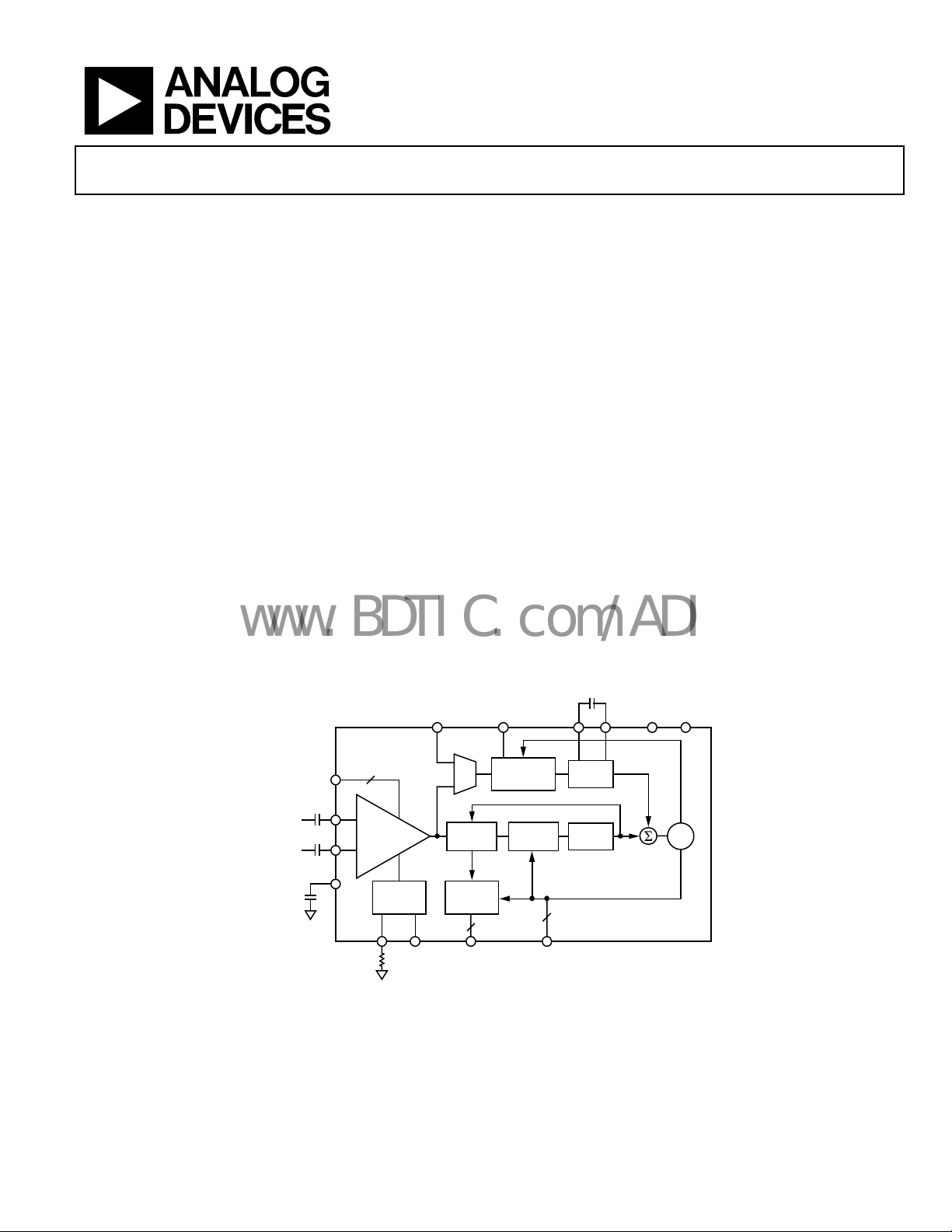
GENERAL DESCRIPTION
The ADN2804 provides the receiver functions of quantization,
signal level detect, clock and data recovery, and data retiming
for 622 Mbps NRZ data. The ADN2804 automatically locks to
622 Mbps data without the need for an external reference clock
or programming. In the absence of input data, the output clock
drifts no more than ±5%. All SONET jitter requirements are
met, including jitter transfer, jitter generation, and jitter
tolerance. All specifications are quoted for −40°C to +85°C
ambient temperature, unless otherwise noted.
This device, together with a PIN diode and a TIA preamplifier,
n implement a highly integrated, low cost, low power fiber
ca
optic receiver.
The receiver’s front-end loss-of-signal (LOS) detector circuit
dicates when the input signal level falls below a user-adjustable
in
threshold. The LOS detect circuit has hysteresis to prevent chatter
at the output.
The ADN2804 is available in a compact 5 mm × 5 mm,
32-lead LFCS
P.
FUNCTIONAL BLOCK DIAGRAM
REFCLKP/REFCLKN
(OPTIO NAL)
SLICEP/SLICEN
PIN
NIN
VREF
Rev. 0
Information furnished by Analog Devices is believed to be accurate and reliable. However, no
responsibility is assumed by Anal og Devices for its use, nor for any infringements of patents or ot her
rights of third parties that may result from its use. Specifications subject to change without notice. No
license is granted by implication or otherwise under any patent or patent rights of Analog Devices.
Trademarks and registered trademarks are the property of their respective owners.
2
QUANTIZER
LOS
DETECT
LOSTHRADJ CLKOUTP/
PHASE
SHIFTER
RE-TIMING
DATAOUTP/
DATAOUTN
DATA
2
Figure 1.
LOL
FREQUENCY
DETECT
PHASE
DETECT
CLKOUTN
One Technology Way, P.O. Box 9106, Norwood, MA 02062-9106, U.S.A.
Tel: 781.329.4700 www.analog.com
Fax: 781.461.3113 ©2006 Analog Devices, Inc. All rights reserved.
LOOP
FILTER
LOOP
FILTER
2
VCC VEECF1 CF2
ADN2804
VCO
5801-001
Page 2

ADN2804
www.BDTIC.com/ADI
TABLE OF CONTENTS
Features.............................................................................................. 1
Jitter Specifications......................................................................... 13
Applications....................................................................................... 1
General Description ......................................................................... 1
Functional Block Diagram .............................................................. 1
Revision History ............................................................................... 2
Specifications..................................................................................... 3
Jitter Specifications....................................................................... 4
Output and Timing Specifications ............................................. 5
Absolute Maximum Ratings............................................................ 6
Thermal Characteristics .............................................................. 6
ESD Caution.................................................................................. 6
Timing Characteristics..................................................................... 7
Pin Configuration and Function Descriptions............................. 8
Typical Performance Characteristics ............................................. 9
2
I
C Interface Timing and Internal Register Description........... 10
Terminology .................................................................................... 12
Theory of Operation ...................................................................... 14
Functional Description.................................................................. 16
Frequency Acquisition............................................................... 16
Limiting Amplifier ..................................................................... 16
Slice Adjust.................................................................................. 16
Loss-of-Signal (LOS) Detector ................................................. 16
Lock Detector Operation .......................................................... 17
SQUELCH Modes...................................................................... 17
2
I
C Interface ................................................................................ 17
Reference Clock (Optional) ...................................................... 19
Applications Information.............................................................. 21
PCB Design Guidelines ............................................................. 21
DC-Coupled Application.......................................................... 23
Outline Dimensions....................................................................... 24
Ordering Guide .......................................................................... 24
REVISION HISTORY
2/06—Revision 0: Initial Version
Rev. 0 | Page 2 of 24
Page 3
ADN2804
www.BDTIC.com/ADI
SPECIFICATIONS
TA = T
unless otherwise noted.
Table 1.
Parameter Conditions Min Typ Max Unit
QUANTIZER—DC CHARACTERISTICS
QUANTIZER—AC CHARACTERISTICS
QUANTIZER—SLICE ADJUSTMENT
LOSS-OF-SIGNAL (LOS) DETECT
R
R
R
LOSS-OF-LOCK (LOL) DETECT
ACQUISITION TIME
DATA RATE READBACK ACCURACY
POWER SUPPLY VOLTAGE 3.0 3.3 3.6 V
POWER SUPPLY CURRENT Locked to 622.08 Mbps 128 mA
OPERATING TEMPERATURE RANGE –40 +85 °C
1
PIN and NIN should be differentially driven and ac-coupled for optimum sensitivity.
2
When ac-coupled, the LOS assert and deassert times are dominated by the RC time constant of the ac coupling capacitor and the 50 Ω input termination of the
ADN2804 input stage.
MIN
to T
, VCC = V
MAX
MIN
to V
, VEE = 0 V, CF = 0.47 μF, SLICEP = SLICEN = VEE, input data pattern: PRBS 223 − 1,
MAX
Input Voltage Range @ PIN or NIN, dc-coupled 1.8 2.8 V
Peak-to-Peak Differential Input PIN − NIN 2.0 V
Input Common-Mode Level DC-coupled (see Figure 27, Figure 28, and Figure 29) 2.3 2.5 2.8 V
Differential Input Sensitivity 223 − 1 PRBS, ac-coupled,1 BER = 1 × 10
–10
6 3.3 mV p-p
Input Offset 500 μV
Input RMS Noise BER = 1 × 10
–10
290 μV rms
Data Rate 622 Mbps
Output Clock Range Absence of input data 622 ± 5% MHz
S11 @ 622 MHz −15 dB
Input Resistance Differential 100 Ω
Input Capacitance 0.65 pF
Gain SLICEP − SLICEN = ±0.5 V 0.10 0.11 0.13 V/V
Differential Control Voltage Input SLICEP − SLICEN −0.95 +0.95 V
Control Voltage Range DC level @ SLICEP or SLICEN VEE 0.95 V
Slice Threshold Offset 1 mV
Loss-of-Signal Detect Range (see Figure 6) R
= 0 Ω 14.9 16.7 18.4 mV
THRESH
= 100 kΩ 2.6 3.5 4.4 mV
THRESH
Hysteresis (Electrical) OC-12
= 0 Ω 6.2 6.9 7.7 dB
THRESH
= 100 kΩ 4.1 6.1 8.1 dB
THRESH
LOS Assert Time DC-coupled
LOS Deassert Time DC-coupled
2
2
500 ns
400 ns
VCO Frequency Error for LOL Assert With respect to nominal 1000 ppm
VCO Frequency Error for LOL Deassert With respect to nominal 250 ppm
LOL Response Time OC-12 200 μs
Lock to Data Mode OC-12 2.0 ms
Optional Lock to REFCLK Mode 20.0 ms
Fine Readback In addition to REFCLK accuracy
OC-12 100 ppm
Rev. 0 | Page 3 of 24
Page 4
ADN2804
www.BDTIC.com/ADI
JITTER SPECIFICATIONS
TA = T
unless otherwise noted.
Table 2.
Parameter Conditions Min Typ Max Unit
PHASE-LOCKED LOOP CHARACTERISTICS
30 Hz
300 Hz
25 kHz 2.5 UI p-p
250 kHz
1
Jitter tolerance of the ADN2804 at these jitter frequencies is better than what the test equipment is able to measure.
to T
MIN
Jitter Transfer Bandwidth OC-12 75 130 kHz
Jitter Peaking OC-12 0 0.03 dB
Jitter Generation OC-12, 12 kHz to 5 MHz 0.001 0.003 UI rms
0.011 0.026 UI p-p
Jitter Tolerance OC-12, 223 − 1 PRBS
, VCC = V
MAX
MIN
to V
, VEE = 0 V, CF = 0.47 μF, SLICEP = SLICEN = VEE, input data pattern: PRBS 223 − 1,
MAX
1
1
1
100 UI p-p
44 UI p-p
1.0 UI p-p
Rev. 0 | Page 4 of 24
Page 5
ADN2804
www.BDTIC.com/ADI
OUTPUT AND TIMING SPECIFICATIONS
Table 3.
Parameter Conditions Min Typ Max Unit
LVDS OUTPUT CHARACTERISTICS
(CLKOUTP/CLKOUTN, DATAOUTP/DATAOUTN)
Output Voltage High VOH (see Figure 3) 1475 mV
Output Voltage Low VOL (see Figure 3) 925 mV
Differential Output Swing VOD (see Figure 3) 250 320 400 mV
Output Offset Voltage VOS (see Figure 3) 1125 1200 1275 mV
Output Impedance Differential 100 Ω
LVDS Outputs’ Timing
Rise Time 20% to 80% 115 220 ps
Fall Time 80% to 20% 115 220 ps
Setup Time TS (see Figure 2), OC-12 760 800 840 ps
Hold Time TH (see Figure 2), OC-12 760 800 840 ps
I2C INTERFACE DC CHARACTERISTICS LVCMOS
Input High Voltage VIH 0.7 VCC V
Input Low Voltage VIL 0.3 VCC V
Input Current VIN = 0.1 VCC or VIN = 0.9 VCC −10.0 +10.0 μA
Output Low Voltage VOL, IOL = 3.0 mA 0.4 V
I2C INTERFACE TIMING See Figure 11
SCK Clock Frequency 400 kHz
SCK Pulse Width High t
SCK Pulse Width Low t
Start Condition Hold Time t
Start Condition Setup Time t
Data Setup Time t
Data Hold Time t
SCK/SDA Rise/Fall Time TR/TF 20 + 0.1 Cb
Stop Condition Setup Time t
Bus Free Time Between a Stop and a Start t
REFCLK CHARACTERISTICS Optional lock to REFCLK mode
Input Voltage Range @ REFCLKP or REFCLKN
V
V
Minimum Differential Input Drive 100 mV p-p
Reference Frequency 10 160 MHz
Required Accuracy 100 ppm
LVTTL DC INPUT CHARACTERISTICS
Input High Voltage VIH 2.0 V
Input Low Voltage VIL 0.8 V
Input High Current IIH, VIN = 2.4 V 5 μA
Input Low Current IIL, VIN = 0.4 V −5 μA
LVTTL DC OUTPUT CHARACTERISTICS
Output High Voltage VOH, IOH = −2.0 mA 2.4 V
Output Low Voltage VOL, IOL = +2.0 mA 0.4 V
1
Cb = total capacitance of one bus line in picofarads. If used with Hs-mode devices, faster fall times are allowed.
600 ns
HIGH
1300 ns
LOW
600 ns
HD;STA
600 ns
SU;STA
100 ns
SU;DAT
300 ns
HD;DAT
600 ns
SU;STO
1300 ns
BUF
0 V
IL
VCC V
IH
1
300 ns
Rev. 0 | Page 5 of 24
Page 6
ADN2804
www.BDTIC.com/ADI
ABSOLUTE MAXIMUM RATINGS
TA = T
0.47 μF, SLICEP = SLICEN = VEE, unless otherwise noted.
Table 4.
Parameter Rating
Supply Voltage (VCC) 4.2 V
Minimum Input Voltage (All Inputs) VEE − 0.4 V
Maximum Input Voltage (All Inputs) VCC + 0.4 V
Maximum Junction Temperature 125°C
Storage Temperature Range −65°C to +150°C
MIN
to T
, VCC = V
MAX
MIN
to V
, VEE = 0 V, CF =
MAX
Stress above those listed under Absolute Maximum Ratings may
ca
use permanent damage to the device. This is a stress rating
only; functional operation of the device at these or any other
conditions above those indicated in the operational sections of
this specification is not implied. Exposure to absolute
maximum rating conditions for extended periods may affect
device reliability.
THERMAL CHARACTERISTICS
Thermal Resistance
32-lead LFCSP, 4-layer board with exposed paddle soldered to
VEE, θ
= 28°C/W.
JA
ESD CAUTION
ESD (electrostatic discharge) sensitive device. Electrostatic charges as high as 4000 V readily accumulate on
the human body and test equipment and can discharge without detection. Although this product features
proprietary ESD protection circuitry, permanent damage may occur on devices subjected to high energy
electrostatic discharges. Therefore, proper ESD precautions are recommended to avoid performance
degradation or loss of functionality.
Rev. 0 | Page 6 of 24
Page 7
ADN2804
www.BDTIC.com/ADI
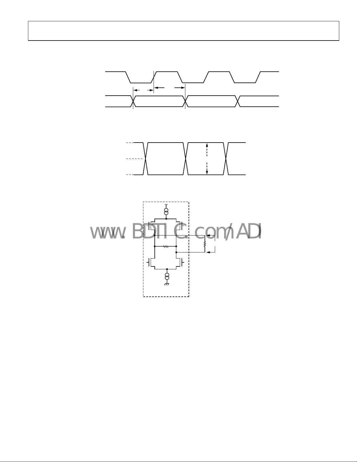
TIMING CHARACTERISTICS
CLKOUTP
T
T
S
DATAOUTP/
DATAOUTN
V
OH
H
Figure 2. Output Timing
DIFFERENTIAL CLKOUTP/ N, DATAOUTP/N
05801-002
V
OS
V
OL
|VOD|
5801-032
Figure 3. Differential Output Specifications
5mA
R
LOAD
V
100Ω
5mA
SIMPLIFIED LVDS
OUTPUT STAGE
100Ω
DIFF
05801-033
Figure 4. Differential Output Stage
Rev. 0 | Page 7 of 24
Page 8
ADN2804
www.BDTIC.com/ADI
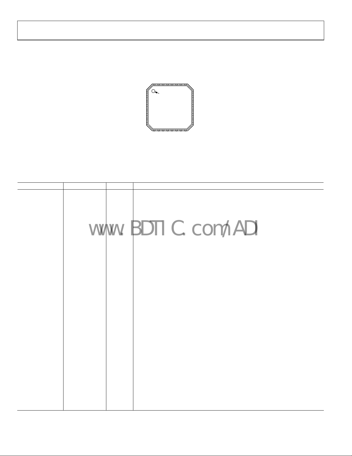
PIN CONFIGURATION AND FUNCTION DESCRIPTIONS
32 TEST2
31 VCC
30 VEE
29 DATAOUTP
28 DATAOUTN
27 SQUELCH
26 CLKOUTP
25 CLKOUTN
TEST1 1
VCC 2
VREF 3
NIN 4
PIN 5
SLICEP 6
SLICEN 7
VEE 8
* THERE IS AN EXPOSED PAD ON THE BOTTOM OF
THE PACKAGE THAT MUST BE CONNECT ED TO GND.
PIN 1
INDICATOR
ADN2804*
TOP VIEW
(Not to Scale)
VCC 12
THRADJ 9
REFCLKP 10
REFCLKN 11
CF2 14
VEE 13
CF1 15
LOL 16
24 VCC
23 VEE
22 LOS
21 SDA
20 SCK
19 SADDR5
18 VCC
17 VEE
05801-004
Figure 5. Pin Configuration
Table 5. Pin Function Descriptions
Pin No. Mnemonic Type
1 TEST1 Connect to VCC.
2 VCC P Power for Limiting Amplifier, LOS.
3 VREF AO Internal VREF Voltage. Decouple to GND with a 0.1 μF capacitor.
4 NIN AI Differential Data Input. CML.
5 PIN AI Differential Data Input. CML.
6 SLICEP AI Differential Slice Level Adjust Input.
7 SLICEN AI Differential Slice Level Adjust Input.
8 VEE P GND for Limiting Amplifier, LOS.
9 THRADJ AI LOS Threshold Setting Resistor.
10 REFCLKP DI Differential REFCLK Input. 10 MHz to 160 MHz.
11 REFCLKN DI Differential REFCLK Input. 10 MHz to 160 MHz.
12 VCC P VCO Power.
13 VEE P VCO GND.
14 CF2 AO Frequency Loop Capacitor.
15 CF1 AO Frequency Loop Capacitor.
16 LOL DO Loss-of-Lock Indicator. LVTTL active high.
17 VEE P FLL Detector GND.
18 VCC P FLL Detector Power.
19 SADDR5 DI Slave Address Bit 5.
20 SCK DI I2C Clock Input.
21 SDA DI I2C Data Input.
22 LOS DO Loss-of-Signal Detect Output. Active high. LVTTL.
23 VEE P Output Buffer, I2C GND.
24 VCC P Output Buffer, I2C Power.
25 CLKOUTN DO Differential Recovered Clock Output. LVDS.
26 CLKOUTP DO Differential Recovered Clock Output. LVDS.
27 SQUELCH DI Disable Clock and Data Outputs. Active high. LVTTL.
28 DATAOUTN DO Differential Recovered Data Output. LVDS.
29 DATAOUTP DO Differential Recovered Data Output. LVDS.
30 VEE P Phase Detector, Phase Shifter GND.
31 VCC P Phase Detector, Phase Shifter Power.
32 TEST2 Connect to VCC.
Exposed Pad Pad P Connect to GND.
1
Type: P = power, AI = analog input, AO = analog output, DI = digital input, DO = digital output.
1
Description
Rev. 0 | Page 8 of 24
Page 9

ADN2804
www.BDTIC.com/ADI
TYPICAL PERFORMANCE CHARACTERISTICS
16
14
12
10
8
TRIP POINT (mV p-p)
6
4
2
1 10 100 1k 10k 100k
Figure 6. LOS Comparator Trip Point Programming
5801-005
Rev. 0 | Page 9 of 24
Page 10
ADN2804
8
www.BDTIC.com/ADI
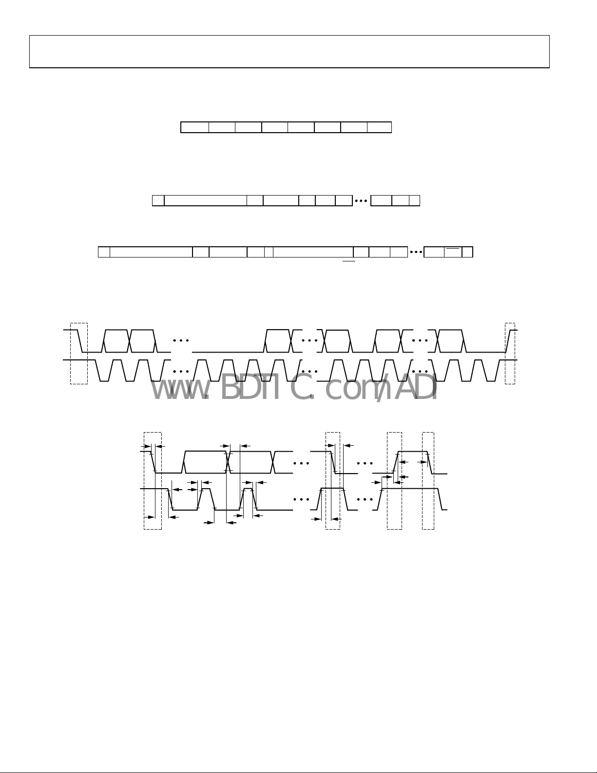
I2C INTERFACE TIMING AND INTERNAL REGISTER DESCRIPTION
SLAVE ADDRESS [6...0]
1A500000X
MSB = 1 SET BY
PIN 19
Figure 7. Slave Address Configuration
R/W
CTRL.
0 = WR
1 = RD
5801-007
S SLAVE ADDR, LSB = 0 (WR) A(S) A(S) A(S)DATASUB ADDR A(S) PDATA
Figure 8. I
2
C Write Data Transfer
5801-00
S
S = START BIT P = STOP BIT
A(S) = ACKNOWLEDGE BY SLAVE A(M) = ACKNOWLEDGE BY MASTER
SSLAVE ADDR, LSB = 0 (WR) SLAVE ADDR, LSB = 1 (RD)A(S) A(S)SUB ADDR A(S) DATA A(M) DATA PA(M)
A(M) = LACK OF ACKNOWLEDG E BY MASTER
2
Figure 9. I
C Read Data Transfer
5801-009
SDA
SCK
START BIT
S
SLAVE ADDRESS SUB ADDRESS DATA
SLADDR[4... 0]
Figure 10. I
SUB ADDR[6...1] DATA[6...1]
2
C Data Transfer Timing
D0D7A0A7A5A6
STOP BIT
ACKACKWR ACK
P
5801-010
t
F
SDA
t
SCK
SS
LOW
t
HD;STA
t
R
t
HD;DAT
t
SU;DAT
Figure 11. I
t
F
t
HIGH
t
SU;STA
2
C Port Timing Diagram
t
HD;STA
t
SU;STO
t
BUF
t
R
PS
5801-011
Rev. 0 | Page 10 of 24
Page 11

ADN2804
www.BDTIC.com/ADI
Table 6. Internal Register Map
1
Reg
Name R/W Addr D7 D6 D5 D4 D3 D2 D1 D0
FREQ0 R 0x0 MSB LSB
FREQ1 R 0x1 MSB LSB
FREQ2 R 0x2 0 MSB LSB
MISC R 0x4 x x LOS status
Static
LO
LOL
L
status
Data rate
measurement
x x
complete
CTRLA W 0x8 F
CTRLB W 0x9
range Data rate/DIV_F
REF
Config
L
LO
Reset
MISC[4]
System
reset
ratio Measure data rate Lock to reference
REF
0
Reset
0 0 0
MISC[2]
CTRLC W 0x11 0 0 0 0 0 Config LOS SQUELCH mode Output boost
1
All writeable registers default to 0x00.
Table 7. Miscellaneous Register, MISC
LOS Status Static LOL LOL Status Data Rate Measurement Complete
D7 D6 D5 D4 D3 D2 D1 D0
x x 0 = No loss of signal 0 = Waiting for next LOL 0 = Locked 0 = Measuring data rate x x
1 = Loss of signal 1 = Static LOL until reset 1 = Acquiring 1 = Measurement complete
Table 8. Control Register, CTRLA
F
Range Data Rate/Div_F
REF
1
Ratio Measure Data Rate Lock to Reference
REF
D7 D6 D5 D4 D3 D2 D1 D0
0 0 19.44 MHz 0 1 0 1 32 Set to 1 to measure data rate 0 = Lock to input data
0 1 38.88 MHz 0 1 0 1 32 1 = Lock to reference clock
1 0 77.76 MHz 0 1 0 1 32
1 1 155.52 MHz 0 1 0 1 32
1
Where DIV_F
is the divided down reference referred to the 10 MHz to 20 MHz band (see the Reference Clock (Optional) section).
REF
Table 9. Control Register, CTRLB
Config LOL Reset MISC[4] System Reset Reset MISC[2]
D7 D6 D5 D4 D3 D2 D1 D0
0 = LOL pin normal operation
1 = LOL pin is static LOL
Write a 1 followed
by 0 to reset MISC[4]
Write a 1 followed by
0 to reset ADN2804
Set to 0
Write a 1 followed
by
0 to reset MISC[2]
Set to 0 Set to 0 Set to 0
Table 10. Control Register, CTRLC
Config LOS SQUELCH Mode Output Boost
D7 D6 D5 D4 D3 D2 D1 D0
0 = Active high LOS
0 = Squelch data outputs and
0 = Default output swing Set to 0 Set to 0 Set to 0 Set to 0 Set to 0
clock outputs
1 = Active low LOS
1 = Squelch data outputs or
1 = Boost output swing
clock outputs
Rev. 0 | Page 11 of 24
Page 12
ADN2804
V
V
www.BDTIC.com/ADI
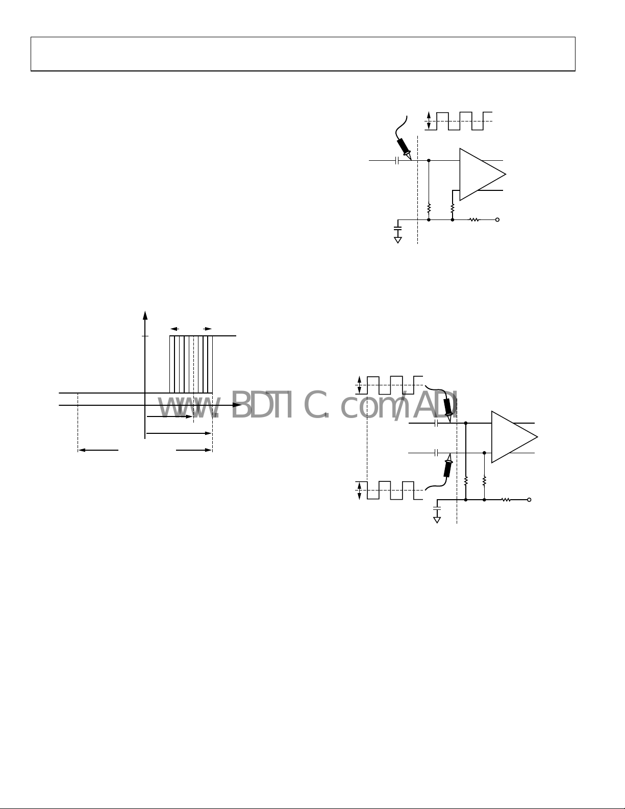
TERMINOLOGY
VREF
10mV p-p
ADN2804
50Ω
SCOPE
PROBE
+
QUANTIZER
–
50Ω
3kΩ
VREF
2.5V
05801-013
Input Sensitivity and Input Overdrive
Sensitivity and overdrive specifications for the quantizer involve
fset voltage, gain, and noise. The relationship between the
of
logic output of the quantizer and the analog voltage input is
shown in
th
Figure 12. For sufficiently large positive input voltage,
e output is always Logic 1; similarly, for negative inputs, the
output is always Logic 0. However, the transitions between
output Logic Level 1 and output Logic Level 0 are not at
precisely defined input voltage levels, but occur over a range of
input voltages. Within this range of input voltages, the output
may be either 1 or 0, or it may even fail to attain a valid logic
state. The width of this zone is determined by the input voltage
noise of the quantizer. The center of the zone is the quantizer
input offset voltage. Input overdrive is the magnitude of signal
required to guarantee the correct logic level with 1 × 10
−10
confidence level.
OUTPUT
1
0
NOISE
SCOPE
PROBE
PIN
Figure 13. Single-Ended Sensitivity Measurement
When the ADN2804 is driven differentially (see Figure 14),
sensitivity seems to improve if observing the quantizer input
with an oscilloscope probe. This is an illusion caused by the use
of a single-ended probe. A 5 mV p-p signal appears to drive the
ADN2804 quantizer; however, the single-ended probe measures
only half the signal. The true quantizer input signal is twice this
value, because the other quantizer input is a complementary
signal to the signal being observed.
5mV p-p
REF
OFFSET
OVERDRIVE
SENSITIVITY
(2 × OVERDRIVE)
Figure 12. Input Sensitivity and Input Overdrive
INPUT (V p-p)
05801-012
Single-Ended vs. Differential
AC coupling is typically used to drive the inputs to the
uantizer. The inputs are internally dc biased to a common-
q
mode potential of ~2.5 V. Driving the ADN2804 in a singleended fashion and observing the quantizer input with an
oscilloscope probe at the point indicated in
b
inary signal with an average value equal to the common-mode
Figure 13 shows a
potential and instantaneous values both above and below the
average value. It is convenient to measure the peak-to-peak
amplitude of this signal and call the minimum required value
the quantizer sensitivity. Referring to
wice the overdrive because both positive and negative offsets
t
Figure 13, the sensitivity is
need to be accommodated. The ADN2804 quantizer typically
has 3.3 mV p-p sensitivity.
PIN
NIN
REF
5mV p-p
Figure 14. Differential Sensitivity Measurement
VREF
50Ω
+
QUANTIZER
–
50Ω
3kΩ
2.5V
5801-014
LOS Response Time
LOS response time is the delay between removal of the input
ignal and indication of loss of signal (LOS) at the LOS output,
s
Pin 22. When the inputs are dc-coupled, the LOS assert time of
the AD2804 is 500 ns typical and the deassert time is 400 ns
typical. In practice, the time constant produced by the ac
coupling at the quantizer input and the 50 Ω on-chip input
termination determines the LOS response time.
Rev. 0 | Page 12 of 24
Page 13
ADN2804
R
www.BDTIC.com/ADI
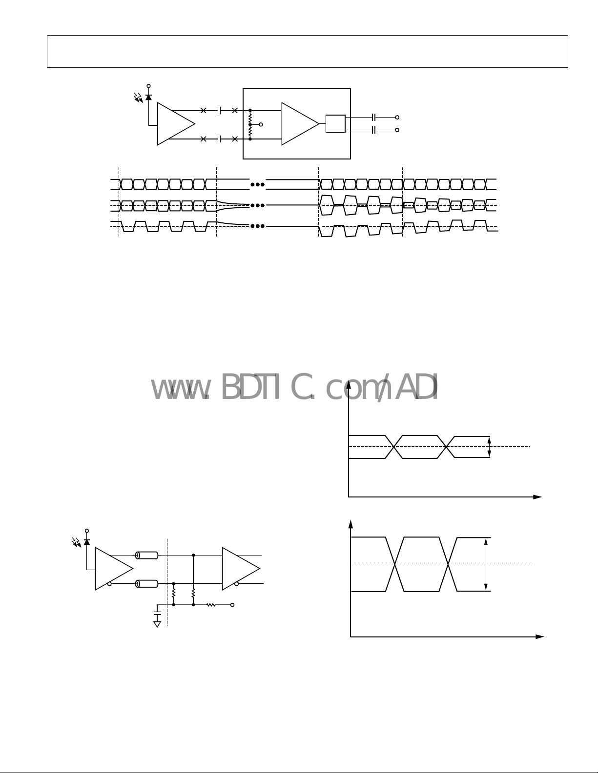
JITTER SPECIFICATIONS
The ADN2804 CDR is designed to achieve the best biterror-rate (BER) performance and to exceed the jitter
transfer, generation, and tolerance specifications proposed
for SONET/SDH equipment defined in the Telcordia
Technologies specification.
Jitter is the dynamic displacement of digital signal edges from
eir long-term average positions, measured in unit intervals
th
(UI), where 1 UI = 1 bit period. Jitter on the input data can
cause dynamic phase errors on the recovered clock sampling
edge. Jitter on the recovered clock causes jitter on the
retimed data.
The following sections briefly summarize the specifications of
ji
tter generation, transfer, and tolerance in accordance with the
Telcordia document (GR-253-CORE, Issue 3, September 2000)
for the optical interface at the equipment level and the
ADN2804 performance with respect to those specifications.
Jitter Generation
The jitter generation specification limits the amount of jitter
hat can be generated by the device with no jitter and wander
t
applied at the input. For SONET devices, the jitter generated
must be less than 0.01 UI rms and less than 0.1 UI p-p.
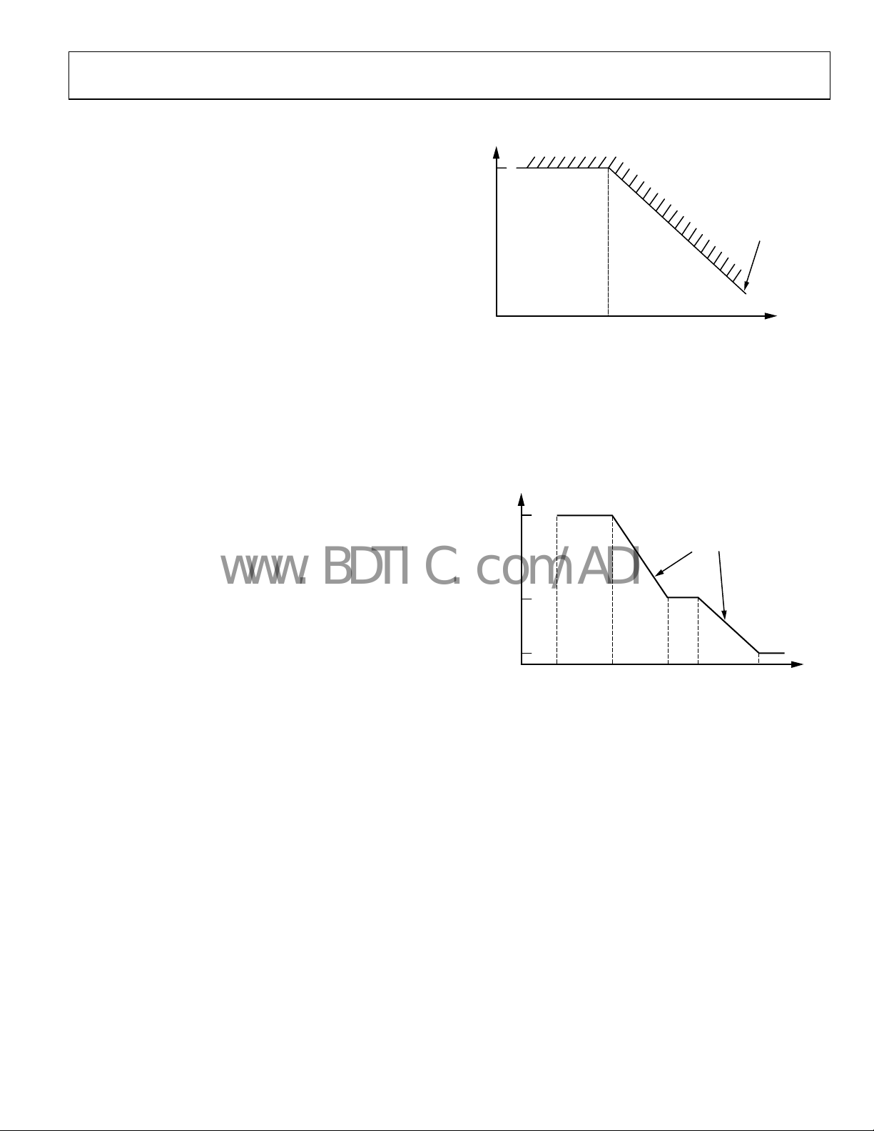
Jitter Transfer
The jitter transfer function is the ratio of the jitter on the output
nal to the jitter applied on the input signal vs. the frequency.
sig
This parameter measures the amount of jitter on an input signal
that can be transferred to the output signal (see
nt is limited.
amou
Figure 15). This
0.1
SLOPE = –20dB/ DECADE
JITTER G AIN (dB)
ACCEPTABLE
RANGE
JITTER FREQUENCY (kHz)
Figure 15. Jitter Transfer Curve
f
C
Jitter Tolerance
The jitter tolerance is defined as the peak-to-peak amplitude of
t
he sinusoidal jitter applied on the input signal, which causes a
1 dB power penalty. This is a stress test intended to ensure that
no additional penalty is incurred under the operating
conditions (see
15.00
1.50
AMPLITUDE (UI p-p)
0.15
INPUT JITTE
Figure 16).
SLOPE = –20dB/DECADE
f
0
Figure 16. SONET Jitter Tolerance Mask
f
1
JITTER FREQUENCY (kHz)
f2f
3
f
4
5801-015
5801-016
Rev. 0 | Page 13 of 24
Page 14

ADN2804
R
www.BDTIC.com/ADI
THEORY OF OPERATION
The ADN2804 is a delay- and phase-locked loop circuit for
clock recovery and data retiming from an NRZ encoded data
stream. The phase of the input data signal is tracked by two
separate feedback loops, which share a common control voltage.
A high speed delay-locked loop path uses a voltage controlled
phase shifter to track the high frequency components of input
jitter. A separate phase control loop, composed of the VCO,
tracks the low frequency components of input jitter. The initial
frequency of the VCO is set by yet a third loop that compares
the VCO frequency with the input data frequency and sets the
coarse tuning voltage. The jitter tracking phase-locked loop
controls the VCO by the fine-tuning control.
The delay and phase loops together track the phase of the input
da
ta signal. For example, when the clock lags the input data, the
phase detector drives the VCO to a higher frequency and
increases the delay through the phase shifter; both of these
actions serve to reduce the phase error between the clock and
the data. The faster clock picks up phase, whereas the delayed
data loses phase. Because the loop filter is an integrator, the
static phase error is driven to 0°.
X(s)
INPUT
DATA
RECOVERED
CLOCK
d = PHASE DETECTOR GAIN
o = VCO GAIN
c = LOOP INTEGRATOR
psh = PHASE SHI FTER GAI N
n = DIVIDE
ATI O
psh
e(s)
d/sc
Z(s)
JITTER TRANSFER FUNCTION
Z(s)
=
X(s)
2
s
TRACKING ERROR T RANSFER FUNCTION
e(s)
=
X(s)
2
s
Figure 17. PLL/DLL Architecture
o/s
1/n
1
n psh
cn
s+ 1
+
o
do
2
s
d psh
do
s++
c
cn
JITTER PEAKING
IN ORDI NARY PLL
5801-017
Another view of the circuit is that the phase shifter implements
t
he zero required for frequency compensation of a second-order
phase-locked loop, and this zero is placed in the feedback path;
therefore, it does not appear in the closed-loop transfer
function. Jitter peaking in a conventional second-order phaselocked loop is caused by the presence of this zero in the closedloop transfer function. Because this circuit has no zero in the
closed-loop transfer, jitter peaking is minimized.
The delay and phase loops together simultaneously provide
wi
deband jitter accommodation and narrow-band jitter
filtering. The linearized block diagram in Figure 17 shows that
he jitter transfer function, Z(s)/X(s), provides excellent second-
t
order low-pass filtering. Note that the jitter transfer has no zero,
unlike an ordinary second-order phase-locked loop. This means
that the main PLL loop has virtually no jitter peaking (see
Figure 18), making this circuit ideal for signal regenerator
pplications, where jitter peaking in a cascade of regenerators
a
can contribute to hazardous jitter accumulation.
The error transfer, e(s)/X(s), has the same high-pass form as an
ord
inary phase-locked loop. This transfer function can be
optimized to accommodate a significant amount of wideband
jitter, because the jitter transfer function, Z(s)/X(s), provides the
narrow-band jitter filtering.
ADN2804
JITTER GAIN (dB)
o
n psh
Figure 18. Jitter Response vs. Conventional PLL
d psh
c
FREQUENCY (kHz)
Z(s)
X(s)
5801-018
The delay and phase loops contribute to overall jitter accommodation. At low frequencies of input jitter on the data signal,
the integrator in the loop filter provides high gain to track large
jitter amplitudes with small phase error. In this case, the VCO is
frequency modulated, and jitter is tracked as in an ordinary
phase-locked loop. The amount of low frequency jitter that can
be tracked is a function of the VCO tuning range. A wider
tuning range gives larger accommodation of low frequency
jitter. The internal loop control voltage remains small for small
phase errors; therefore, the phase shifter remains close to the
center of its range and thus contributes little to the low
frequency jitter accommodation.
Rev. 0 | Page 14 of 24
Page 15

ADN2804
www.BDTIC.com/ADI
At medium jitter frequencies, the gain and tuning range of the
VCO are not large enough to track input jitter. In this case, the
VCO control voltage becomes large and saturates, and the VCO
frequency dwells at one extreme of its tuning range. The size of
the VCO tuning range, therefore, has only a small effect on the
jitter accommodation. The delay-locked loop control voltage is
now larger; therefore, the phase shifter takes on the burden of
tracking the input jitter. The phase shifter range, in UI, can be
seen as a broad plateau on the jitter tolerance curve. The phase
shifter has a minimum range of 2 UI at all data rates.
The gain of the loop integrator is small for high jitter
f
requencies; therefore, larger phase differences are needed to
increase the loop control voltage enough to tune the range of
the phase shifter. However, large phase errors at high jitter
frequencies cannot be tolerated. In this region, the gain of the
integrator determines the jitter accommodation. Because the
gain of the loop integrator declines linearly with frequency,
jitter accommodation is lower with higher jitter frequency. At
the highest frequencies, the loop gain is very small, and little
tuning of the phase shifter can be expected. In this case, jitter
accommodation is determined by the eye opening of the input
data, the static phase error, and the residual loop jitter generation.
The jitter accommodation is roughly 0.5 UI in this region. The
corner frequency between the declining slope and the flat region
is the closed-loop bandwidth of the delay-locked loop, which is
roughly 1.0 MHz at 622 Mbps.
Rev. 0 | Page 15 of 24
Page 16
ADN2804
www.BDTIC.com/ADI
FUNCTIONAL DESCRIPTION
FREQUENCY ACQUISITION
The ADN2804 acquires frequency from the data. The lock
detector circuit compares the frequency of the VCO and the
frequency of the incoming data. When these frequencies differ
by more than 1000 ppm, LOL is asserted. This initiates a frequency
acquisition cycle. When the VCO frequency is within 250 ppm
of the data frequency, LOL is deasserted.
Once LOL is deasserted, the frequency-locked loop is turned
o
ff. The PLL/DLL pulls the VCO frequency in the rest of the
way until the VCO frequency equals the data frequency.
The frequency loop requires a single external capacitor between
CF1 a
nd CF2, Pin 14 and Pin 15. A 0.47 μF ± 20%, X7R ceramic
chip capacitor with <10 nA leakage current is recommended.
Leakage current of the capacitor can be calculated by dividing
the maximum voltage across the 0.47 μF capacitor, ~3 V, by the
insulation resistance of the capacitor. The insulation resistance
of the 0.47 μF capacitor should be greater than 300 MΩ.
LIMITING AMPLIFIER
The limiting amplifier has differential inputs (PIN/NIN) that
are internally terminated with 50 Ω to an on-chip voltage
reference (VREF = 2.5 V typically). The inputs are typically
ac-coupled externally, although dc coupling is possible as long
as the input common-mode voltage remains above 2.5 V (see
Figure 27 to Figure 29 in the Applications Information section).
I
nput offset is factory trimmed to achieve better than 3.3 mV
typical sensitivity with minimal drift. The limiting amplifier can
be driven differentially or in a single-ended fashion.
SLICE ADJUST
The quantizer slicing level can be offset by ±100 mV to mitigate
the effect of amplified spontaneous emission (ASE) noise or duty
cycle distortion by applying a differential voltage input of up to
±0.95 V to the SLICEP and SLICEN inputs. If no adjustment of
the slice level is needed, SLICEP and SLICEN should be tied to
VEE. The gain of the slice adjustment is ~0.11 V/V.
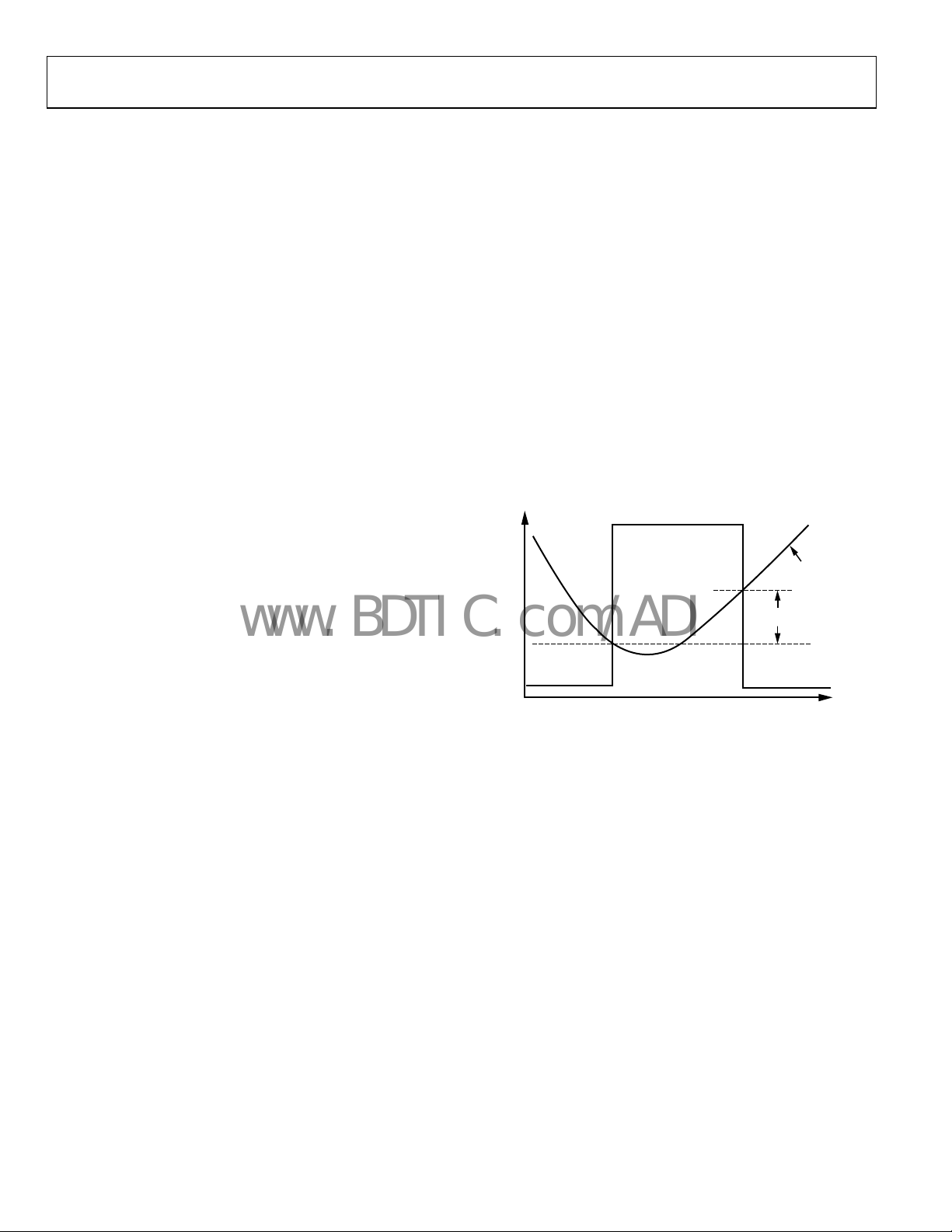
LOSS-OF-SIGNAL (LOS) DETECTOR
The receiver front-end LOS detector circuit detects when the
input signal level falls below a user-adjustable threshold. The
threshold is set with a single external resistor from Pin 9,
THRADJ, to VEE. The LOS comparator trip point vs. the
resistor value is shown in
N2804 drops below the programmed LOS threshold, the
AD
output of the LOS detector, LOS (Pin 22), is asserted to Logic 1.
The LOS detector’s response time is ~500 ns by design, but is
dominated by the RC time constant in ac-coupled applications.
The LOS pin defaults to active high. However, setting Bit
CTRLC[2] to 1, configures the LOS pin as active low.
There is typically 6 dB of electrical hysteresis designed into the
LO
S detector to prevent chatter on the LOS pin. If the input
level drops below the programmed LOS threshold causing the
LOS pin to assert, the LOS pin deasserts after the input level
increases to 6 dB (2×) above the LOS threshold (see Figure 19).
)
DIFF
IN PU T VO LTAG E (V
The LOS detector and the SLICE level adjust can be used
simultaneously on the ADN2804. This means that any offset
added to the input signal by the SLICE adjust pins does not affect
the LOS detector’s measurement of the absolute input level.
Figure 6. If the input level to the
LOS OUTPUT
INPUT LEVEL
HYSTERESIS
LOS THRESHOLD
t
Figure 19. LOS Detector Hysteresis
5801-019
Rev. 0 | Page 16 of 24
Page 17
ADN2804
www.BDTIC.com/ADI
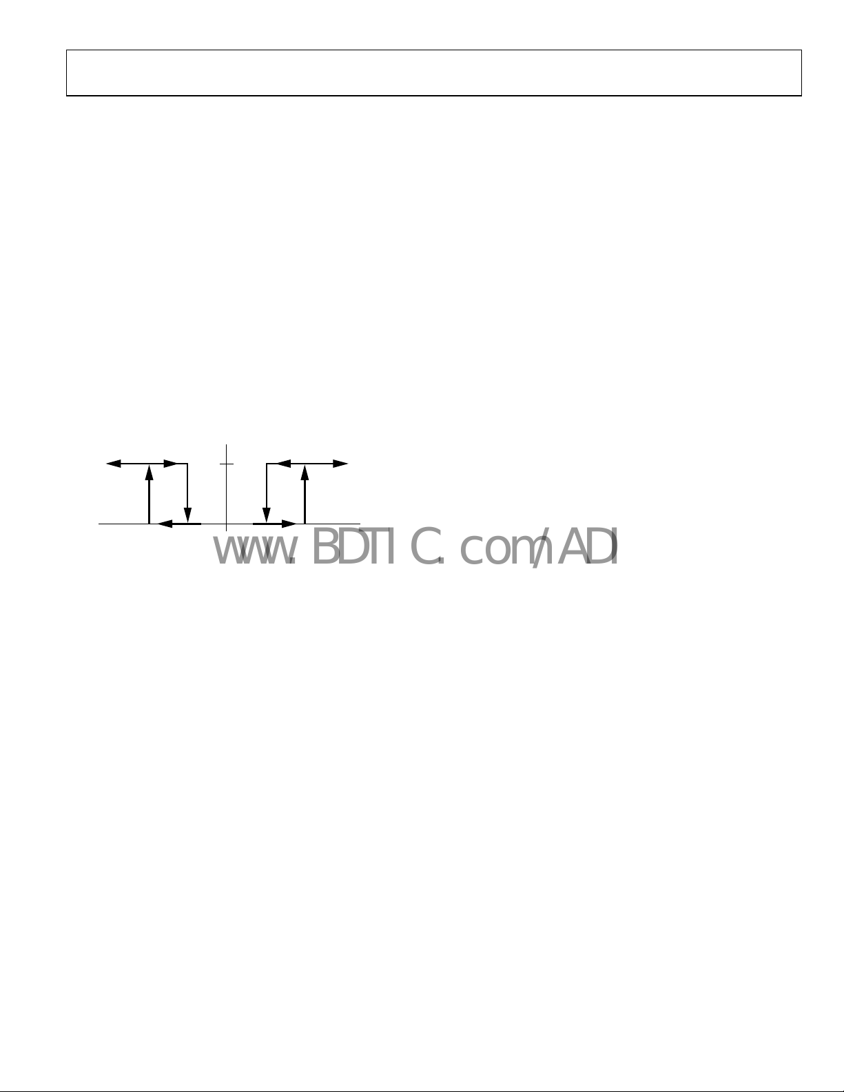
LOCK DETECTOR OPERATION
The lock detector on the ADN2804 has three modes of
operation: normal mode, REFCLK mode, and static LOL mode.
Normal Mode
In normal mode, the ADN2804 is a CDR that locks onto a
622 Mbps data rate without the use of a reference clock as an
acquisition aid. In this mode, the lock detector monitors the
frequency difference between the VCO and the input data
frequency and deasserts the loss of lock signal, which appears
on Pin 16, LOL, when the VCO is within 250 ppm of the data
frequency. This enables the D/PLL, which pulls the VCO
frequency in the remaining amount and acquires phase lock.
Once locked, if the input frequency error exceeds 1000 ppm
(0.1%), the loss-of-lock signal is reasserted and control returns
to the frequency loop, which begins a new frequency
acquisition. The LOL pin remains asserted until the VCO locks
onto a valid input data stream to within 250 ppm frequency
error. This hysteresis is shown in
–1000
Figure 20. Transfer Function of LOL
LOL Detector Operation Using a Reference Clock
In REFCLK mode, a reference clock is used as an acquisition aid
to lock the ADN2804 VCO. Lock-to-reference mode is enabled
by setting CTRLA[0] to 1. The user also needs to write to the
CTRLA[7, 6] and CTRLA[5:2] bits to set the reference
frequency range and the divide ratio of the data rate with
respect to the reference frequency. For more details, see the
Reference Clock (Optional) section. In this mode, the lock
ector monitors the difference in frequency between the
det
divided down VCO and the divided down reference clock. The
loss-of-lock signal, which appears on Pin 16, LOL, is deasserted
when the VCO is within 250 ppm of the desired frequency. This
enables the D/PLL, which pulls the VCO frequency in the
remaining amount with respect to the input data and acquires
phase lock. Once locked, if the input frequency error exceeds
1000 ppm (0.1%), the loss-of-lock signal is reasserted and
control returns to the frequency loop, which reacquires with
respect to the reference clock. The LOL pin remains asserted
until the VCO frequency is within 250 ppm of the desired
frequency. This hysteresis is shown in
Figure 20.
LOL
1
0–250 250 1000 f
Figure 20.
VCO
(ppm)
ERROR
5801-020
Static LOL Mode
The ADN2804 implements a static LOL feature that indicates if
a loss-of-lock condition has ever occurred. This feature remains
asserted, even if the ADN2804 regains lock, until the static LOL
bit is manually reset. The I
2
C register bit, MISC[4], is the static
LOL bit. If there is ever an occurrence of a loss-of-lock condition,
this bit is internally asserted to logic high. The MISC[4] bit remains
high even after the ADN2804 has reacquired lock to a new data
rate. This bit can be reset by writing a 1 followed by 0 to I
2
C
Register Bit CTRLB[6]. Once reset, the MISC[4] bit remains
deasserted until another loss-of-lock condition occurs.
Writ i ng a 1 to I
2
C Register Bit CTRLB[7] causes the LOL pin,
Pin 16, to become a static LOL indicator. In this mode, the LOL
pin mirrors the contents of the MISC[4] bit and has the
functionality described in the previous paragraph. The CTRLB[7]
bit defaults to 0. In this mode, the LOL pin operates in the
normal operating mode, that is, it is asserted only when the
ADN2804 is in acquisition mode and deasserts when the
ADN2804 has reacquired lock.
SQUELCH MODES
Two modes for the SQUELCH pin are available with the
ADN2804: squelch data outputs and clock outputs mode and
squelch data outputs or clock outputs mode. Squelch data outputs
and clock outputs mode is selected when CTRLC[1] is 0 (default
mode). In this mode, when the SQUELCH input, Pin 27, is driven
to a TTL high state, both the data outputs (DATAOUTN and
DATAOUTP) and the clock outputs (CLKOUTN and CLKOUTP)
are set to the zero state to suppress downstream processing. If
the squelch function is not required, Pin 27 should be tied to VEE.
Squelch data outputs or
clock outputs mode is selected when
CTRLC[1] is 1. In this mode, when the SQUELCH input is
driven to a high state, the DATAOUTN and DATAOUTP pins
are squelched. When the SQUELCH input is driven to a low
state, the CLKOUTN and CLKOUTP pins are squelched. This is
especially useful in repeater applications, where the recovered
clock may not be needed.
I2C INTERFACE
The ADN2804 supports a 2-wire, I2C-compatible serial bus
driving multiple peripherals. Two inputs, serial data (SDA) and
serial clock (SCK), carry information to and from any device
connected to the bus. Each slave device is recognized by a
unique address. The ADN2804 has two possible 7-bit slave
addresses for both read and write operations. The MSB of the
7-bit slave address is factory programmed to 1. B5 of the slave
address is set by Pin 19, SADDR5. Slave Address Bits [4:0] are
defaulted to all 0s. The slave address consists of the seven MSBs
of an 8-bit word. The LSB of the word either sets a read or write
operation (see
hile Logic 0 corresponds to a write operation.
w
Figure 7). Logic 1 corresponds to a read operation,
Rev. 0 | Page 17 of 24
Page 18

ADN2804
www.BDTIC.com/ADI
To control the device on the bus, the following protocol must be
followed. First, the master initiates a data transfer by establishing a start condition, defined by a high-to-low transition on
SDA while SCK remains high. This indicates that an address/
data stream follows. All peripherals respond to the start condition
and shift the next eight bits (the 7-bit address and the R/W bit).
The bits are transferred from MSB to LSB. The peripheral that
recognizes the transmitted address responds by pulling the data
line low during the ninth clock pulse. This is known as an
acknowledge bit. All other devices withdraw from the bus at
this point and maintain an idle condition. The idle condition is
where the device monitors the SDA and SCK lines, waiting for
the start condition and correct transmitted address. The R/W
bit determines the direction of the data. Logic 0 on the LSB of
the first byte means that the master writes information to the
peripheral. Logic 1 on the LSB of the first byte means that the
master reads information from the peripheral.
The ADN2804 acts as a standard slave device on the bus. The data
n the SDA pin is eight bits long, supporting the 7-bit addresses
o
plus the R/W bit. The ADN2804 has eight subaddresses to enable
the user-accessible internal registers (see
10). It, therefore, interprets the first byte as the device address
a
nd the second byte as the starting subaddress. Auto-increment
mode is supported, allowing data to be read from or written to
the starting subaddress and each subsequent address without
manually addressing the subsequent subaddress. A data transfer
is always terminated by a stop condition. The user can also
access any unique subaddress register on a one-by-one basis
without updating all registers.
Tabl e 6 through Tab le
Stop and start conditions can be detected at any stage of the
ta transfer. If these conditions are asserted out of sequence
da
with normal read and write operations, they cause an immediate
jump to the idle condition. During a given SCK high period, the
user should issue one start condition, one stop condition, or a
single stop condition followed by a single start condition. If an
invalid subaddress is issued by the user, the ADN2804 does not
issue an acknowledge and returns to the idle condition. If the
user exceeds the highest subaddress while reading back in autoincrement mode, then the highest subaddress register contents
continue to be output until the master device issues a no acknowledge. This indicates the end of a read. In a no-acknowledge
condition, the SDATA line is not pulled low on the ninth pulse.
See
Figure 8 and Figure 9 for sample write and read data transfers
a
nd Figure 10 for a more detailed timing diagram.
Additional Features Available via the I2C Interface
LOS Configuration
The LOS detector output, Pin 22, can be configured to be either
active high or active low. If CTRLC[2] is set to Logic 0 (default),
the LOS pin is active high when a loss-of-signal condition is
detected. Writing a 1 to CTRLC[2] configures the LOS pin to be
active low when a loss-of-signal condition is detected.
System Reset
A frequency acquisition can be initiated by writing a 1 followed
by a 0 to the I
frequency acquisition while keeping the ADN2804 in its
previously programmed operating mode, as set in Registers
CTRL[A], CTRL[B], and CTRL[C].
2
C Register Bit CTRLB[5]. This initiates a new
Rev. 0 | Page 18 of 24
Page 19
ADN2804
V
www.BDTIC.com/ADI
REFERENCE CLOCK (OPTIONAL)
A reference clock is not required to perform clock and data
recovery with the ADN2804; however, support for an optional
reference clock is provided. The reference clock can be driven
differentially or in a single-ended fashion. If the reference
clock is not being used, REFCLKP should be tied to VCC, and
REFCLKN can be left floating or tied to VEE (the inputs are
internally terminated to VCC/2). See
23 for sample configurations.
The REFCLK input buffer accepts any differential signal with a
eak-to-peak differential amplitude of greater than 100 mV (for
p
example, LVPECL or LVDS) or a standard single-ended, low
voltage TTL input, providing maximum system flexibility.
Phase noise and duty cycle of the reference clock are not
critical, and 100 ppm accuracy is sufficient.
ADN2804
REFCLKP
10
11
REFCLKN
Figure 21. Differential REFCLK Configuration
CC
REFCLKP
CLK
OSC
OUT
REFCLKN
Figure 22. Single-Ended REFCLK
VCC
REFCLKP
NC
REFCLKN
Figure 23. No REFCLK Configur
ADN2804
ADN2804
10
11
100kΩ
Figure 21 through Figure
BUFFER
100kΩ
100kΩ
BUFFER
100kΩ
100kΩ
Configuration
BUFFER
100kΩ
ation
VCC/2
VCC/2
VCC/2
5801-021
5801-022
5801-023
There are two mutually exclusive uses, or modes, of the
reference clock. The reference clock can be used either to help
the ADN2804 lock onto data or to measure the frequency of the
incoming data to within 0.01%. The modes are mutually
exclusive because in the first use the user knows exactly what
the data rate is and wants to force the part to lock onto only that
data rate, and in the second use the user does not know what
the data rate is and wants to measure it.
Lock-to-reference mode is enabled by writing a 1 to I
2
C Register
Bit CTRLA[0]. Fine data rate readback mode is enabled by
writing a 1 to I
2
C Register Bit CTRLA[1]. Writing a 1 to both of
these bits at the same time causes an indeterminate state and is
not supported.
Using the Reference Clock to Lock onto Data
In this mode, the ADN2804 locks onto a frequency derived
from the reference clock according to
Data Rate/2
CTRLA[5:2]
= REFCLK/2
CTRLA[7, 6]
The user must provide a reference clock that is a function of the
ta rate. By default, the ADN2804 expects a reference clock of
da
19.44 MHz. Other options are 38.88 MHz, 77.76 MHz, and
155.52 MHz, which are selected by programming CTRLA[7, 6].
CTRLA[5:2] should be programmed to [0101] for all cases.
Table 11. CTRLA Settings
CTRLA[7, 6] Range (MHz) CTRLA[5:2] Ratio
00 19.44 0101 25
01 38.88 0101 25
10 77.76 0101 25
11 155.52 0101 25
For example, if the reference clock frequency is 38.88 MHz and the
input data rate is 622.08 Mbps, CTRLA[7, 6] is set to [01] to
produce a divided-down reference clock of 19.44 MHz, and
CTRLA[5:2] is set to [0101], that is, 5, because
622.08 Mbps/19.44 MHz = 2
5
In this mode, if the ADN2804 loses lock for any reason, it relocks
o
nto the reference clock and continues to output a stable clock.
While the ADN2804 is operating in lock-to-reference mode,
a
0 to 1 transition should be written into the CTRLA[0] bit to
initiate a lock-to-reference clock command.
Rev. 0 | Page 19 of 24
Page 20
ADN2804
(
www.BDTIC.com/ADI
Using the Reference Clock to Measure Data Frequency
The user can also provide a reference clock to measure the
recovered data frequency. In this case, the user provides a
reference clock, and the ADN2804 compares the frequency of
the incoming data to the incoming reference clock and returns a
ratio of the two frequencies to within 0.01% (100 ppm) accuracy.
The accuracy error of the reference clock is added to the accuracy
of the ADN2804 data rate measurement. For example, if a 100 ppm
accuracy reference clock is used, the total accuracy of the measurement is within 200 ppm.
The reference clock can range from 10 MHz to 160 MHz.
y default, the ADN2804 expects a reference clock between
B
10 MHz and 20 MHz. If the reference clock is between 20 MHz
and 40 MHz, 40 MHz and 80 MHz, or 80 MHz and 160 MHz,
the user must configure the ADN2804 for the correct reference
frequency range by setting two bits of the CTRLA register,
CTRLA[7, 6]. Using the reference clock to determine the frequency
of the incoming data does not affect the manner in which the
part locks onto data. In this mode, the reference clock is used
only to determine the frequency of the data.
Prior to reading back the data rate using the reference clock, the
CTRL
A[7, 6] bits must be set to the appropriate frequency
range with respect to the reference clock being used. A fine data
rate readback is then executed as follows:
3. Read back MISC[2]. If it is 0, the measurement is not
complete. If it is 1, the measurement is complete and the
data rate can be read back on FREQ[22:0]. The time for a
data rate measurement is typically 80 ms.
4. Read back t
FREQ0[7:0].
The data rate can be determined by
DATARATE
where:
FREQ[22:0] is th
FREQ1[7:0], and FREQ0[7:0] (LSB byte).
f
is the data rate (Mbps).
DATARATE
is the REFCLK frequency (MHz).
f
REFCLK
SEL_RATE is the setting from CTRLA[7, 6].
For example, if the reference clock frequency is 32 MHz,
EL_RATE = 1, because the reference frequency falls into the
S
20 MHz to 40 MHz range, setting CTRLA[7, 6] to [01],.
Assume for this example that the input data rate is 622.08 Mb/s
(OC12). After following Step 1 through Step 4, the value that is
read back on FREQ[22:0] = 0x9B851, which is equal to 637 × 10
Plugging this value into the equation yields
637e3 × 32e6/2
he data rate from FREQ2[6:0], FREQ1[7:0], and
)_14(
RATESEL
+
[]
×=
e reading from FREQ2[6:0] (MSB byte,
(14 + 1)
= 622.08 Mbps
fFREQf
REFCLK
)
2/0.22
3
.
1. W
rite a 1 to CTRLA[1]. This enables the fine data rate
measurement capability of the ADN2804. This bit is level
sensitive and can perform subsequent frequency measurements
without being reset.
2. Res
et MISC[2] by writing a 1 followed by a 0 to CTRLB[3].
This initiates a new data rate measurement.
Table 12.
D22 D21 ... D17 D16 D15 D14 ... D9 D8 D7 D6 ... D1 D0
FREQ2[6:0] FREQ1[7:0] FREQ0[7:0]
If subsequent frequency measurements are required, CTRLA[1]
hould remain set to 1. It does not need to be reset. The
s
measurement process is reset by writing a 1 followed by a 0 to
CTRLB[3]. This initiates a new data rate measurement. Follow
Step 2 through Step 4 to read back the new data rate.
Note that a data rate readback is valid only if LOL is low. If LOL
is hig
h, the data rate readback is invalid.
Rev. 0 | Page 20 of 24
Page 21

ADN2804
(
=
V
www.BDTIC.com/ADI
APPLICATIONS INFORMATION
PCB DESIGN GUIDELINES
Proper RF PCB design techniques must be used for optimal
performance.
Power Supply Connections and Ground Planes
Use of one low impedance ground plane is recommended. The
VEE pins should be soldered directly to the ground plane to
reduce series inductance. If the ground plane is an internal
plane and connections to the ground plane are made through
vias, multiple vias can be used in parallel to reduce the series
inductance, especially on Pin 23, which is the ground return for
the output buffers. The exposed pad should be connected to the
GND plane using plugged vias so that solder does not leak
through the vias during reflow.
Use of a 22 μF electrolytic capacitor between VCC and VEE is
ecommended at the location where the 3.3 V supply enters the
r
PCB. When using 0.1 μF and 1 nF ceramic chip capacitors, they
should be placed between ADN2804 supply pins VCC and VEE,
as close as possible to the ADN2804 VCC pins.
If connections to the supply and ground are made through
ias, the use of multiple vias in parallel helps to reduce series
v
inductance, especially on Pin 24, which supplies power to the
high speed CLKOUTP/CLKOUTN and DATAOUTP/
DATAOUTN output buf fers. Refer to
r
ecommended connections.
Figure 24 for the
By placing the power supply and GND planes adjacent to each
ther and using close spacing between the planes, excellent high
o
frequency decoupling can be realized. The capacitance is given
by
)
pF/0.88εrdAC
PLANE
where:
ε
is the dielectric constant of the PCB material.
r
A is the area of the overlap of power and GND planes (cm
2
).
d is the separation between planes (mm).
For FR-4, ε
C
PLANE
= 4.4 and d = 0.25 mm; therefore,
r
~ 15.5A (pF)
CC
0.1µF
+
TIA
1nF
0.1µF
50Ω
50Ω
0.1µF22µF 1nF
TEST2
TEST1
1
VCC
2
VREF
3
NIN
4
PIN
5
SLICEP
VEE
VCC
R
0.1µF
6
7
8
THRADJ
TH
SLICEN
1.6µF
1.6µF
Figure 24. Typical ADN2804 Applications Circuit
50Ω TRANSMISSION L INES
OUTP
TAOUTP
CC
SQUELCH
DATAOUTN
DA
VEE
V
31
32
EXPOSED PAD
TIED OFF TO
VEE PLANE
WITH VIAS
9
10
REFCLKP
1nF
CLK
29
28
27
30
11
13
14
12
CF1
CF2
VEE
VCC
REFCLKN
NC
0.47µF ±20%
>300MΩ INSUL ATION RESISTANCE
DATAOUTP
DATAOUTN
CLKOUTP
CLKOUTN
CLKOUTN
25
26
VCC
24
VEE
23
LOS
22
SDA
21
SCK
20
SADDR5
19
VCC
18
VEE
17
15
LOL
1nF
16
µC
VCC
0.1µF1nF
2
C CONTROLL ER
I
2
C CONTROLL ER
I
VCC
0.1µF
µC
05801-031
Rev. 0 | Page 21 of 24
Page 22

ADN2804
VCC
www.BDTIC.com/ADI
Transmission Lines
Minimizing reflections in the ADN2804 requires use of 50 Ω
transmission lines for all pins with high frequency input and
output signals, including PIN, NIN, CLKOUTP, CLKOUTN,
DATAOUTP, and DATAOUTN (also REFCLKP and REFCLKN,
if a high frequency reference clock is used, such as 155 MHz). It
is also necessary for the PIN/NIN input traces to be matched in
length and for the CLKOUTP/CLKOUTN and
DATAOUTP/DATAOUTN output traces to be matched in
length to avoid skew between the differential traces.
The high speed inputs, PIN and NIN, are internally terminated
ith 50 Ω to an internal reference voltage (see Figure 25).
w
A 0.1 μF
is recommended between VREF, Pin 3, and GND to
provide an ac ground for the inputs.
Choosing AC Coupling Capacitors
AC coupling capacitors at the input (PIN, NIN) and output
(DATAOUTP, DATAOUTN) of the ADN2804 can be optimized
for the application. When choosing the capacitors, the time
constant formed with the two 50 Ω resistors in the signal path
must be considered. When a large number of consecutive
identical digits (CIDs) are applied, the capacitor voltage can
droop due to baseline wander (see
dep
endent jitter (PDJ).
Figure 26), causing pattern-
The user must determine how much droop is tolerable and
hoose an ac coupling capacitor based on that amount of droop.
c
The amount of PDJ can then be approximated based on the
capacitor selection. The actual capacitor value selection can
require some trade-offs between droop and PDJ.
As with any high speed, mixed-signal design, take care to keep
all h
igh speed digital traces away from sensitive analog nodes.
ADN2804
C
IN
50Ω
TIA
Figure 25. ADN2804 AC-Coupled Input Configuration
50Ω
0.1µF
PIN
C
IN
NIN
VREF
3Ω
2.5V
5801-026
Soldering Guidelines for Lead Frame Chip Scale Package
The lands on the 32-lead LFCSP are rectangular. The printed
circuit board (PCB) pad for these should be 0.1 mm longer than
the package land length and 0.05 mm wider than the package
land width. The land should be centered on the pad. This
ensures that the solder joint size is maximized. The bottom of
the chip scale package has a central exposed pad. The pad on
the PCB should be at least as large as this exposed pad. The user
must connect the exposed pad to VEE using plugged vias so
that solder does not leak through the vias during reflow. This
ensures a solid connection from the exposed pad to VEE.
For example, assuming that 2% droop can be tolerated, the
um differential droop is 4%. Normalizing to V p-p:
maxim
−t/τ
Droop = ΔV = 0
.04 V = 0.5 V p-p (1 − e
); therefore, τ = 12t
where:
he RC time constant (C is the ac coupling capacitor, R =
τ is t
100 Ω seen by C).
t is the total discharge time, which is equal to nT, where n is the
number of CIDs, and T is the bit period.
The capacitor value can then be calculated by combining the
quations for τ and t:
e
C = 12
nT/R
Once the capacitor value is selected, the PDJ can be
a
pproximated as
PDJ
pspp
= 0.5 tr(1 − e
(−nT/RC)
)/0.6
where:
PDJ
is the amount of pattern-dependent jitter allowed
pspp
(<0.01 UI p-p typical).
t
is the rise time, which is equal to 0.22/BW,
r
where BW ~ 0.7 (bit rate).
Note that this expression for t
is accurate only for the inputs.
r
The output rise time for the ADN2804 is ~100 ps regardless of
the data rate.
Rev. 0 | Page 22 of 24
Page 23
ADN2804
V
V
V
www.BDTIC.com/ADI
V1
V1b
V2
V2b
DIFF
V
= V2–V2b
DIFF
VTH = ADN2804 QUANTIZER T HRESHOLD
NOTES:
1. DURING DATA PATTERNS WITH HIG H TRANSITION DENSITY, DIFFERENTIAL DC VOLTAGE AT V1 AND V2 IS Z ERO.
2. WHEN THE OUT PUT OF THE TIA GOES TO CID, V1 AND V1b ARE DRIVEN TO DI FFERENT DC L EVELS. V2 AND V2b DISCHARGE T O THE
VREF LEVEL, WHICH EFFECTI VELY I NTRODUCES A DIFFERENTIAL DC OFFSET ACROSS THE AC COUPLING CAPACITORS.
3. WHEN THE BURST OF DATA STARTS AGAIN, THE DIFF ERENTIAL DC OFF SET ACROSS THE AC COUPLING CAPACITORS IS APPLIED TO
THE INPUT LEVELS CAUSING A DC SHIFT IN THE DIFFERENTIAL INPUT. THIS SHIFT IS LARGE ENOUGH SUCH THAT ONE OF THE STATES,
EITHER HIG H OR LOW DE PENDING ON T HE LEVELS OF V1 AND V1b WHEN T HE TIA WENT TO CID, IS CANCELED OUT. THE QUANTI ZER
DOES NOT RECO GNIZE T HIS AS A VALID STATE .
4. THE DC OFF SET SLOWLY DI SCHARGES UNTI L THE DIFFERENTIAL INPUT VOLTAGE EXCEEDS T HE SENSIT IVITY OF T HE ADN2804. THE
QUANTIZER CAN RECO GNIZE BOTH HIGH AND LOW STATES AT THIS PO INT.
CC
C
IN
V1
TIA
1
V1b
V2
C
IN
V2b
234
PIN
50Ω
50Ω
NIN
ADN2804
+
LIMAMP
V
REF
–
CDR
C
OUT
C
OUT
DATAOUTP
DATAOUTN
VREF
VTH
5801-027
Figure 26. Example of Baseline Wander
DC-COUPLED APPLICATION
The inputs to the ADN2804 can also be dc-coupled. This may
be necessary in burst mode applications, where there are long
periods of CIDs, and baseline wander cannot be tolerated. If the
inputs to the ADN2804 are dc-coupled, care must be taken not
to violate the input range and common-mode level requirements of the ADN2804 (see
co
upling is required and the output levels of the TIA do not
adhere to the levels shown in
erformed and/or an attenuator must be placed between the
p
TIA outputs and the ADN2804 inputs.
CC
TIA
Figure 27. DC-Coupled Application
Figure 27 through Figure 29). If dc
Figure 28, level shifting must be
50Ω
50Ω
0.1µF
ADN2804
PIN
NIN
50Ω 50Ω
VREF
3kΩ
2.5V
05801-028
PIN
INPUT (V)
NIN
V p-p = PI N – NIN = 2×VSE = 10mV AT SENSITIVITY
Figure 28. Minimum Allowed DC-Cou
PIN
INPUT (V)
NIN
V p-p = PIN – NIN = 2×VSE = 2.0V MAX
Figure 29. Maximum Allowed DC-Cou
= 5mV MIN
V
SE
= 2.3V MI N
V
CM
(DC-COUPLED)
pled Input Levels
= 1.0V MAX
V
SE
= 2.3V
V
CM
(DC-COUPLED)
pled Input Levels
5801-029
5801-030
Rev. 0 | Page 23 of 24
Page 24

ADN2804
www.BDTIC.com/ADI
OUTLINE DIMENSIONS
0.60 MAX
25
24
EXPOSED
PAD
(BOTTOM VIEW)
17
16
32
1
8
9
3.50 REF
PIN 1
INDICATOR
3.45
3.30 SQ
3.15
0.25 MIN
PIN 1
INDICATOR
1.00
0.85
0.80
12° MAX
SEATING
PLANE
5.00
BSC SQ
TOP
VIEW
0.80 MAX
0.65 TYP
0.30
0.23
0.18
COMPLIANT TO JEDEC STANDARDS MO-220-VHHD-2
4.75
BSC SQ
0.20 REF
0.05 MAX
0.02 NOM
0.60 MAX
0.50
BSC
0.50
0.40
0.30
COPLANARITY
0.08
Figure 30. 32-Lead Frame Chip Scale Package [LFCSP_VQ]
mm × 5 mm Body, Very Thin Quad
5
(CP-32-3)
Dimensions shown in millimeters
ORDERING GUIDE
Model Temperature Range Package Description Package Option
ADN2804ACPZ
ADN2804ACPZ-500RL7
ADN2804ACPZ-RL7
EVAL-ADN2804EB Evaluation Board
1
Z = Pb-free part.
Purchase of licensed I2C components of Analog Devices or one of its sublicensed Associated Companies conveys a license for the purchaser under the Philips I2C Patent
Rights to use these components in an I2C system, provided that the system conforms to the I2C Standard Specification as defined by Philips.
©2006 Analog Devices, Inc. All rights reserved. Trademarks and
registered trademarks are the property of their respective owners.
D05801–0–2/06(0)
1
1
1
−40°C to +85°C 32-Lead LFCSP_VQ CP-32-3
−40°C to +85°C 32-Lead LFCSP_VQ, Tape-Reel, 500 pieces CP-32-3
−40°C to +85°C 32-Lead LFCSP_VQ, Tape-Reel, 1500 pieces CP-32-3
Rev. 0 | Page 24 of 24
 Loading...