

10.7 Gbps Active Back-Termination,
A
Preliminary Technical Data
FEATURES
Up to 10.7 Gbps operation
Very low power: I
Typical 24 ps rise/fall times
Full back-termination of output transmission lines
Cross Point Adjust Function
PECL/CML-compatible data inputs
Bias current range: 2 mA to 25 mA
Differential modulation current range: 2 mA to 23 mA
Automatic laser shutdown (ALS)
3.3 V operation
Compact 3 mm × 3 mm LFCSP package
Voltage–input control for bias and modulation currents
XFP-compliant bias current monitor
APPLICATIONS
SONET OC-192 optical transceivers
SDH STM-64 optical transceivers
10 Gb Ethernet optical transceivers
XFP/X2/XENPAK/MSA 300 optical modules
= 65 mA
CC
Differential VCSEL Driver
ADN2530
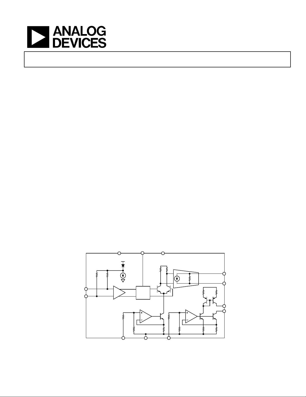
GENERAL DESCRIPTION
The ADN2530 VCSEL driver is designed for direct modulation
of packaged VCSELs. The active back-termination technique
provides excellent matching with the output transmission lines
while reducing the power dissipation in the output stage. The
small package provides the optimum solution for compact
modules where VCSELs are packaged in low pin-count optical
subassemblies.
The differential data inputs are PECL/CML-compatible and
terminated with an internal 100 Ω differential resistor. This
minimizes signal reflections to the data signal source.
The modulation and bias currents are programmable via the
MSET and BSET control pins. By driving these pins with
control voltages, the user has the flexibility to implement
various average power and extinction ratio control schemes,
including closed-loop control and look-up tables. The eye cross
point in the output eye diagram is adjustable via the cross point
adjust (CPA) control voltage input.
The automatic laser shutdown feature allows the user to turn
on/off the bias and modulation currents by driving the ALS pin
with the proper logic levels.
FUNCTIONAL BLOCK DIAGRAM
800Ω
Adjust
200Ω
CP
Cross
Point
VCC ALS
VCC
50Ω 50Ω
GND
DATAP
DATAN
MSET GND BSET
Rev. PrB
Information furnished by Analog Devices is believed to be accurate and reliable.
However, no responsibility is assumed by Analog Devices for its use, nor for any
infringements of patents or other rights of third parties that may result from its use.
Specifications subject to change without notice. No license is granted by implication
or otherwise under any patent or patent rights of Analog Devices. Trademarks and
registered trademarks are the property of their respective owners.
VCC
Figure 1.
The product is available in a space saving 3 mm × 3 mm LFCSP
package specified from −40°C to +85°C.
ADN2530
100ΩIMOD
VCC
800Ω
200Ω
One Technology Way, P.O. Box 9106, Norwood, MA 02062-9106, U.S.A.
Tel: 781.329.4700 www.analog.com
Fax: 781.326.8703 © 2005 Analog Devices, Inc. All rights reserved.
200Ω 10Ω
IMODP
IMODN
IBMON
IBIAS
02461-001

ADN2530 Preliminary Technical Data
TABLE OF CONTENTS
Specifications..................................................................................... 3
Absolute Maximum Ratings............................................................ 5
Package Thermal Specifications................................................. 5
ESD Caution.................................................................................. 5
Pin Configuration and Function Descriptions............................. 6
Typical Performance Characteristics ............................................. 7
Theory of Operation ........................................................................ 9
General........................................................................................... 9
Input Stage..................................................................................... 9
Bias Current .................................................................................. 9
Automatic Laser Shutdown (ALS) ........................................... 10
Modulation Current................................................................... 10
REVISION HISTORY
x/04—Revision PrB: Second Version
Cross Point Adjust...................................................................... 12
Power Consumption .................................................................. 12
Applications Information.............................................................. 14
Typical Application Circuit....................................................... 14
Layout Guidelines....................................................................... 15
Design Example.......................................................................... 15
Headroom Calculations ............................................................ 15
BSET and MSET Pin Voltage Calculation .............................. 15
Outline Dimensions....................................................................... 17
Ordering Guide .......................................................................... 17
Rev. PrB | Page 2 of 17

Preliminary Technical Data ADN2530
SPECIFICATIONS
VCC = VCC
noted. Typical values are specified at 25°C, IMOD = 10 mA, Cross Point Adjust disabled.
Table 1.
Parameter Min Typ Max Unit Test Conditions/Comments
BIAS CURRENT(IBIAS)
Bias Current Range 2 25 mA
Bias current while ALS Asserted 50 µA ALS = high
Compliance Voltage1 0.5 VCC – 1.3 V IBIAS = 25 mA
0.5 VCC – 0.8 V IBIAS = 2 mA
MODULATION CURRENT (IMODP, IMODN)
Modulation Current Range 2 23 mA diff. R
Modulation Current while ALS Asserted 200 µA diff ALS = high
Rise time (20% to 80%)
Fall time (20% to 80%)
Random Jitter
Deterministic Jitter
Cross Point Adjust Range3 35 65 %
Differential |S22| −10 dB 5 Ghz < F < 10 GHz, Z0 = 100 Ω differential
−15 dB F < 5 GHz, Z0 = 100 Ω differential
Compliance Voltage1 VCC − 0.7 VCC + 0.7 V
DATA INPUTS (DATAP, DATAN)
Input Data Rate 10.7 Gbps NRZ
Differential Input Swing 0.4 1.6 V pk-pk diff. Differential ac-coupled
Differential |S11| −15 dB F < 10 GHz, Z0 = 100 Ω differential
Input Termination Resistance 85 100 115 Ω Differential
BIAS CONTROL INPUT (BSET)
BSET Voltage to IBIAS Gain 15 20 24 mA/V
BSET Input Resistance 800 1000 1200 Ω
MODULATION CONTROL INPUT (MSET)
MSET Voltage to IMOD Gain 15 20 24 mA/V
MSET Input Resistance 800 1000 1200 Ω
BIAS MONITOR (IBMON)
IBMON to IBIAS Ratio 50 µA/mA
Accuracy of IBIAS to IBMON Ratio −5.0 +5.0 %
−4.0 +4.0 %
−2.5 +2.5 %
−2 +2 %
AUTOMATIC LASER SHUTDOWN (ALS)
VIH 2.4 V
VIL 0.8 V
IIL −20 +20 µA
IIH 0 200 µA
ALS Assert Time 10 µs
ALS Negate Time 10 µs
POWER SUPPLY
VCC 3.07 3.3 3.53 V
I
27 31 mA V
CC5
I
65 73 mA V
SUPPLY6
1
Refers to the voltage between the pin for which the compliance voltage is specified and GND.
2
The pattern used is composed by a repetitive sequence of eight 1s followed by eight 0s at 10.7 Gbps.
3
Measured using the high speed characterization circuit shown in Figure 3.
4
The pattern used is K28.5 (00111110101100000101) at 10.7 Gbps rate.
5
Only includes current in the ADN2525 VCC pins.
6
Includes current in ADN2525 VCC pins and DC current in IMODP and IMODN pull-up inductors. See section on “Power Consumption” for total supply current
calculation.
to VCC
MIN
2, 3
0.4 0.9 ps rms
3,4
, TA = −40°C to +85°C, 100 Ω differential load impedance, Cross Point Adjust disabled, unless otherwise
MAX
LOAD
2, 3
24 32 ps
2, 3
24 32 ps
7.0 10 ps pk-pk
2 mA ≤ IBIAS < 4 mA, R
4 mA ≤ IBIAS < 8 mA, R
8 mA ≤ IBIAS < 14 mA, R
14 mA ≤ IBIAS < 25 mA, R
Rising edge of ALS to fall of IBIAS and IMOD below 10% of
nominal. See Figure 2
Falling edge of ALS to rise of IBIAS and IMOD above 90% of
nominal. See Figure 2
BSET
BSET
= 35 Ω to 100 Ω differential
= 750 Ω
IBMON
= 750 Ω
IBMON
= 750 Ω
IBMON
= 750 Ω
IBMON
= V
= 0 V
MSET
= V
= 0 V
MSET
Rev. PrB | Page 3 of 17
ADN2530 Preliminary Technical Data
VEEV
V
Z
= 50Ω
0
J2
GND GND GND
J3
GND GND
ALS
IBIAS
AND IMOD
90%
10%
ALS
ASSERT TIME
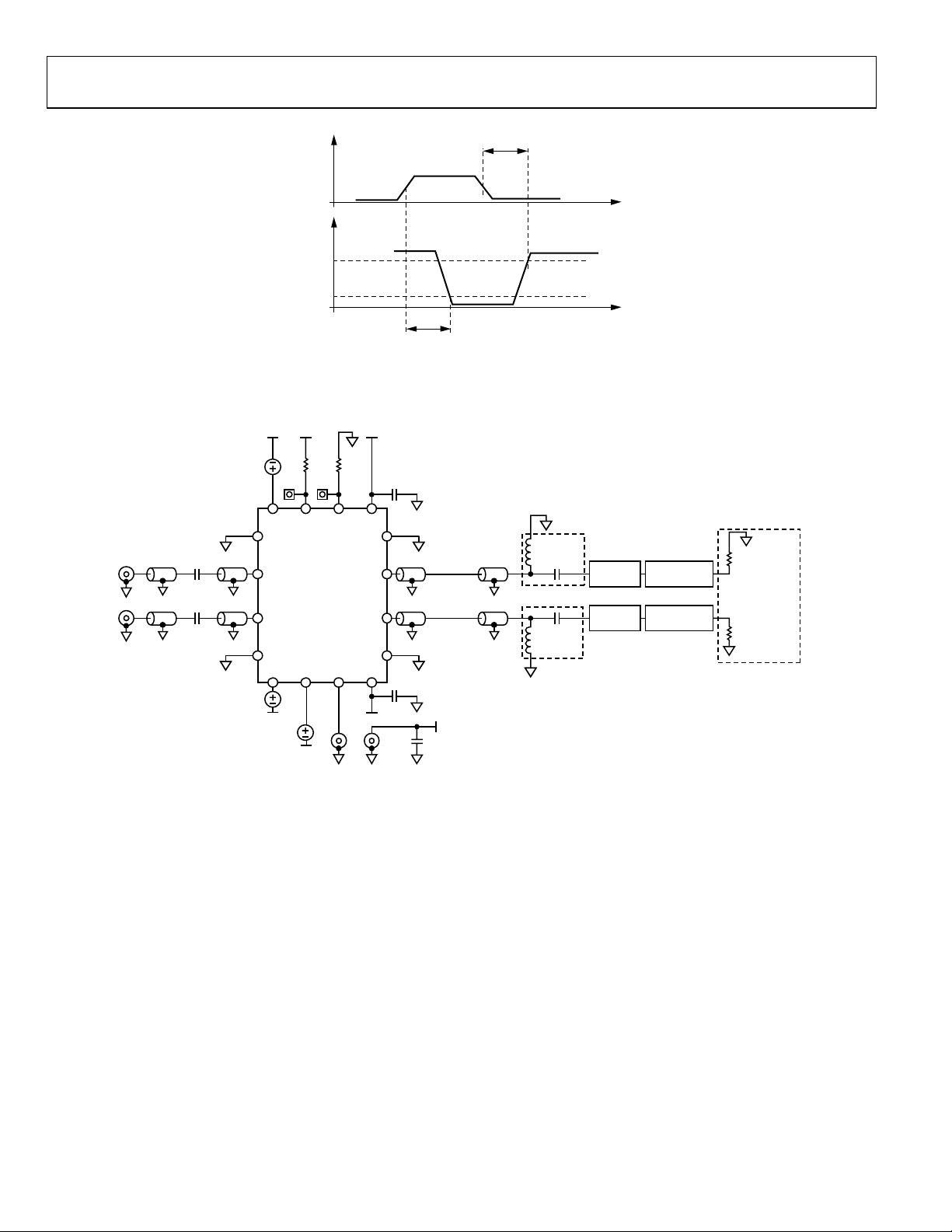
Figure 2. ALS Timing Diagram
EE
TP1
VCC
DATAP
DATAN
VCC
750Ω
TP2
ADN2530
VBSET
BSET IBMON IBIAS GND
GND
Z
= 50Ω Z0 = 50Ω Z0 = 50Ω
0
10nF
10nF
GND
MSET CPA ALS GND
GND
10Ω
IMODP
IMODN
VCC
VCC
EE
10nF
GND
GND
GND
= 50Ω Z0 = 50ΩZ0 = 50ΩZ0 = 50Ω
Z
0
GND
ALS
NEGATE TIME
t
t
02461-002
GND
BIAS TEE
ADAPTOR
GND
ADAPTOR
GND
GNDGND
BIAS TEE
GND
ATTENUATOR
ATTENUATOR
GND
50Ω
OSCILLOSCOPE
50Ω
GND
VMSET
VEE
VCPA
J8 J5
VEE
GND GND GND
VEE
10nF
22µF
GND
VEE
BIAS TEE: Picosecond Pulse Labs Model 5542-219
Adaptor: Pasternack PE-9436 2.92mm female-to-female adaptor
Attenuator: Pasternack PE-7046 2.92mm 20dB attenuator
Figure 3. High Speed Characterization Circuit
02461-003
Rev. PrB | Page 4 of 17
Preliminary Technical Data ADN2530
ABSOLUTE MAXIMUM RATINGS
Table 2.
Parameter Min Max Unit
Supply Voltage—VCC to GND −0.3 +4.2 V
IMODP, IMODN to GND VCC − 1 .5 4.5 V
DATAP, DATAN to GND VCC − 1.8 VCC − 0.4 V
All Other Pins −0.3 VCC + 0.3 V
Junction Temperature 150 °C
Storage Temperature −65 +150 °C
Soldering Temperature
(Less than 10 s)
240 °C
PACKAGE THERMAL SPECIFICATIONS
Table 3.
Parameter Min Typ Max Unit Conditions/Comments
θ
θ
J-TOP
J-PAD
2.6 5.8 10.7 °C/W Thermal resistance from junction to top of package.
65 72.2 79.4 °C/W Thermal resistance from junction to bottom of exposed pad.
Stresses above those listed under Absolute Maximum Ratings
may cause permanent damage to the device. This is a stress
rating only; functional operation of the device at these or any
other conditions above those indicated in the operational
section of this specification is not implied. Exposure to absolute
maximum rating conditions for extended periods may affect
device reliability.
ESD CAUTION
ESD (electrostatic discharge) sensitive device. Electrostatic charges as high as 4000 V readily accumulate on
the human body and test equipment and can discharge without detection. Although this product features
proprietary ESD protection circuitry, permanent damage may occur on devices subjected to high energy
electrostatic discharges. Therefore, proper ESD precautions are recommended to avoid performance
degradation or loss of functionality.
Rev. PrB | Page 5 of 17

ADN2530 Preliminary Technical Data
PIN CONFIGURATION AND FUNCTION DESCRIPTIONS
VCC
DATAN
DATAP
VCC
161514
13
BSET
VCC
IMODP
12
11
10
9
IBMON
IBIAS
GND
02461-016
1
MSET
CPA
ALS
GND
2
3
4
PIN 1
INDICATOR
ADN2530
TOP VIEW
5
678
VCC
IMODN
Figure 4. Pin Configuration
Note: There is an exposed pad on the bottom of the package that must be connected to the VCC or GND plane with filled vias.
Table 4. Pin Function Descriptions
Pin No. Mnemonic I/O Description
1 MSET Input Modulation current control input
2 CPA Input Cross Point Adjust control input
3 ALS Input Automatic laser shutdown
4 GND Power Negative power supply
5 VCC Power Positive power supply
6 IMODN Output Modulation current negative output
7 IMODP Output Modulation current positive output
8 VCC Power Positive power supply
9 GND Power Negative power supply
10 IBIAS Output Bias current output
11 IBMON Output Bias current monitoring output
12 BSET Input Bias current control input
13 VCC Power Positive power supply
14 DATAP Input Data signal positive input
15 DATAN Input Data signal negative input
16 VCC Power Positive power supply
Exposed Pad Pad Power Connect to GND or VCC
Rev. PrB | Page 6 of 17

Preliminary Technical Data ADN2530
TYPICAL PERFORMANCE CHARACTERISTICS
TA = 25°C, VCC = 3.3 V, Cross Point Adjust disabled, unless otherwise noted.
000
000
)
p
a
c
l
000
a
i
t
i
n
I
(
S
P
A
000
C
L
L
A
000
000
000 000 000 000 000 000
TBD
ALL CAPS (Initial cap)
Figure 5. Rise Time v s. IMOD
000
000
)
p
a
c
l
000
a
i
t
i
n
I
(
S
P
A
000
C
L
L
A
000
TBD
000
000
)
p
a
c
l
000
a
i
t
i
n
I
(
S
P
A
000
C
L
L
A
000
000
000 000 000 000 000 000
TBD
ALL CAPS (Initial cap)
Figure 8. Deterministic Jitter vs. IMOD
000
000
)
p
a
c
l
a
000
i
t
i
n
I
(
S
P
A
000
C
L
L
A
000
TBD
000
000 000 000 000 000 000
ALL CAPS (Initial cap)
Figure 6. Fall Time vs. IMOD
000
000
)
p
a
c
l
a
000
i
t
i
n
I
(
S
P
A
000
C
L
L
A
000
000
000 000 000 000 000 000
TBD
ALL CAPS (Initial cap)
Figure 7. Random Jitter vs. IMOD
Rev. PrB | Page 7 of 17
000
000 000 000 000 000 000
ALL CAPS (Initial cap)
Figure 9. Total Supply Current vs. IMOD
000
000
)
p
a
c
l
a
000
i
t
i
n
I
(
S
P
A
000
C
L
L
A
000
000
000 000 000 000 000 000
TBD
ALL CAPS (Initial cap)
Figure 10. Differential |S
|
11

ADN2530 Preliminary Technical Data
000
000
)
p
a
c
l
a
000
i
t
i
n
I
(
S
P
A
000
C
L
L
A
000
000
000 000 000 000 000 000
000
000
)
p
a
c
l
a
000
i
t
i
n
I
(
S
P
A
000
C
L
L
A
000
TBD
ALL CAPS (Initial cap)
Figure 11. Differential |S
TBD
|
22
Figure 14 Electrical Eye Diagram
(Imod=10mA, PRBS31Pattern at 10.3125Gbps)
000
000
)
p
a
c
l
000
a
i
t
i
n
I
(
S
P
A
000
C
L
L
A
000
TBD
000
000
000 000 000 000 000 000
ALL CAPS (Initial cap)
000 00 0 000 000 00 0 000
ALL CAPS (Initial cap)
Figure 15. Electrical eye diagram cross point.
Figure 12. Worst-Case Rise Time Distribution
(VCC = 3.07)
000
000
)
p
a
c
l
a
000
i
t
i
n
I
(
S
P
A
000
C
L
L
A
000
000
000 000 000 000 000 000
Figure 13. Worst-Case Fall Time Distribution
TBD
ALL CAPS (Initial cap)
(VCC = 3.07 V,)
Figure 16. Filtered 10G Ethernet Optical Eye using AOC HFE6192-562 VCSEL
(PRBS31 Pattern at 10.3125Gbps,)
Rev. PrB | Page 8 of 17

Preliminary Technical Data ADN2530
THEORY OF OPERATION
GENERAL
As shown in Figure 1, the ADN2530 consists of an input stage
and two voltage controlled current sources for bias and
modulation. The bias current is available at the IBIAS pin, and
can be monitored at the IBMON pin. The MSET voltage is
converted to current. This current is applied to a differential
pair that switches current into two internal resistors according
to the data signal applied to the driver. The voltage generated
across these resistors is applied to the output stage circuitry,
which produces the differential modulation current that drives
the laser. This output stage also implements the active backmatch circuitry for proper transmission line matching and
power consumption reduction. The ADN2530 can drive a load
having differential impedance ranging from 35 Ω to 100 Ω.
INPUT STAGE
The input stage of the ADN2530 converts the data signal
applied to the DATAP and DATAN pins to a level that ensures
proper operation of the high speed switch. The equivalent
circuit of the input stage is shown in Figure 17.
VCC
DATAP
VCC
DATAN
Figure 17. Equivalent Circuit of the Input Stage
The DATAP and DATAN pins are terminated internally with a
100 Ω differential termination resistor. This minimizes signal
reflections at the input, which could otherwise lead to
degradation in the output eye diagram. The 100 Ω resistor is
built as a combination of two 50 Ω resistors, one for each data
pin, connected to a common-mode voltage source that biasses
the input stage transistors. It is not recommended to drive the
ADN2530 with single-ended data signal sources.
The ADN2530 input stage must be ac-coupled to the signal
source to eliminate the need for matching between the
common-mode voltages of the data signal source and the input
stage of the driver (see Figure 18). The ac-coupling capacitors
should be chosen so that their impedance is less than 50 Ω over
the required frequency range. Generally this is achieved using
capacitor values from 10 nF to 100 nF.
50Ω
50Ω
VCC
02461-017
50Ω 50Ω
DATA SIGNAL SOURCE
Figure 18. AC-Coupling the Data Source to the
ADN2530 Data Inputs
C
C
BIAS CURRENT
The bias current is generated internally using a voltage to
current converter, consisting of an internal operational
amplifier and a transistor as shown in Figure 19.
ADN2530
800Ω
200Ω
GND
Figure 19. Voltage to Current Converter Used to Generate IBIAS
The voltage to current conversion factor is set at 20 mA/V by
the internal resistors. The bias current is monitored using a
current mirror with a gain equal to 1/20, given by the ratio of
the degeneration resistors (10 Ω/200 Ω). The current mirror
output is the IBMON pin that sources the IBIAS/20 current
from VCC. By connecting a 750 Ω resistor between IBMON
and GND, the bias current can be monitored as a voltage across
the resistor. A low temperature coefficient, precision resistor
must be used for the IBMON resistor (R
value of R
due to tolerances, or drift in its value over
IBMON
temperature, contributes to the overall error budget for the
IBIAS monitor voltage. If the IBMON voltage is being
connected to an ADC for A/D conversion, R
placed close to the ADC to minimize errors due to voltage
drops on the ground plane.
VCC
200Ω
ADN2530
DATAP
DATAN
I
BMON
IBMONBSET
IBIAS
I
BIAS
10Ω
). Any error in the
IBMON
should be
IBMON
02461-018
02461-019
Rev. PrB | Page 9 of 17

ADN2530 Preliminary Technical Data
V
A
A
The equivalent circuits of the BSET, IBIAS, and IBMON pins
are shown in Figure 20, Figure 21, and Figure 22.
VCC
BSET
800Ω
200Ω
Figure 20. Equivalent Circuit of the BSET Pin
IBIAS
VCC
10Ω
Figure 21. Equivalent Circuit of the IBIAS Pin
VCC
100Ω
VCC
VCC
CC
500Ω
2kΩ
02461-021
02461-020
V
COMPLIANCE
The function of the inductor L is to isolate the capacitance of
the IBIAS output from the high frequency signal path.
AUTOMATIC LASER SHUTDOWN (ALS)
The ALS pin is a digital input that enables/disables both the bias
and modulation currents, depending on the logic state applied
(see Table 5).
Table 5.
ALS Logic State IBIAS and IMOD
High Disabled
Low Enabled
Floating Enabled
The ALS pin is compatible with 3.3 V CMOS and TTL logic
levels. Its equivalent circuit is shown in Figure 24.
(V) = VCC(V) − 0.75 − 22 × IBIAS(A)
VCC
LS
50kΩ
Figure 24. Equivalent Circuit of the ALS Pin
100Ω
VCC
2kΩ
02461-024
100Ω
VCC
IBMON
02461-022
Figure 22. Equivalent Circuit of the IBMON Pin
The recommended configuration for BSET, IBIAS, and IBMON
is shown in Figure 23.
TO LASER C
IBIAS
ADN2530
BSET
VBSET
IBMON
GND
Figure 23. Recommended Configuration for BSET, IBIAS, and IBMON Pins
THODE
L
IBIAS
R
IBMON
750Ω
02461-023
The circuit used to drive the BSET voltage must be capable of
driving the 1 kΩ input resistance of the BSET pin. For proper
operation of the bias current source, the voltage at IBIAS pin
must be between the compliance voltage specifications for this
pin over supply, temperature, and bias current range. See the
Specifications table. The maximum compliance voltage is
specified for only two bias current levels (2 mA and 25 mA),
but it can be calculated for any bias current using the following
equation:
MODULATION CURRENT
The modulation current can be controlled by applying a dc
voltage to the MSET pin. This voltage is converted into a dc
current by using a voltage to current converter using an
operational amplifier and a bipolar transistor as shown in
Figure 25.
VCC
100ΩIMOD
FROM CPA STAGE
MSET
800Ω
200Ω
GND
ADN2530
Figure 25. Generation of Modulation Current on ADN2530
This dc current is used as a tail current for the differential pair
that generates a high speed voltage across the resistive loads
based on the data signal applied to the input stage (DATAP and
DATAN pins). The high speed differential voltage is applied to
the output stage circuitry that generates the differential
modulation current available at the IMODP and IMODN pins.
The equivalent circuits for MSET, IMODP, and IMODN are
shown in Figure 26 and Figure 27.
IMODP
IMODN
02461-025
Rev. PrB | Page 10 of 17

Preliminary Technical Data ADN2530
V
V
V
V
V
V
The output stage also generates the active back termination,
which provides proper transmission line termination. Active
back termination uses feedback around an active circuit to
synthesize a broadband termination resistance. This provides
excellent transmission line termination, while dissipating less
power than a traditional resistor passive back termination.
CC
MSET
Figure 26. Equivalent Circuit of the MSET Pin
800Ω
200Ω
CC
02461-026
VCC
50
IMODN
Ω
15
IMODP
15
Ω
Ω
Figure 27. Equivalent Circuit of the IMODP and IMODN Pins
50
Ω
VCC
02461-027
The recommended configuration of the MSET, IMODP, and
IMODN pins is shown in Figure 28.
CC
CC
L
L
IMODP
ADN2530
IMODN
Z0 = 50Ω Z0 = 50Ω
Z
= 50Ω Z0 = 50Ω
0
C
LOAD
LCL
31
30.5
30
29.5
29
28.5
28
27.5
27
26.5
26
25.5
25
mA/V
24.5
24
23.5
23
22.5
22
21.5
21
20.5
20
19.5
30 35 40 45 50 55 60 65 70 75 80 85 90 95 100
DIFFERENTIAL LOAD RESISTANCE
Figure 29. MSET Voltage to Modulation Current Ratio vs.
Differential Load Resistance
Using the resistance of the TOSA, the user can calculate the
voltage range that should be applied to the MSET pin to
generate the required modulation current range.
The circuit used to drive the MSET voltage must be capable of
driving the 1 kΩ resistance of the MSET pin. To be able to drive
23 mA modulation currents through the differential load, the
output stage of the ADN2530 (IMODP, IMODN pins) must be
ac-coupled to the load. The voltages at these pins have a dc
component equal to VCC and an ac component with singleended peak-to-peak amplitude of IMOD × 50 Ω. This is the
case even if the load impedance is less than 100 Ω differential,
since the transmission line characteristic impedance sets the
peak-to-peak amplitude. For normal operation, the voltages at
the IMODP and IMODN pins must be within the range shown
in Figure 30. The user must perform headroom calculations to
ensure that the voltages at IMODP and IMODN pins are within
the normal operation region for the required modulation
currents.
V
IMODP, IMODN
VCC
02461-028
CC + 0.7
NORMAL OPERATION REGION
VCC
VMSET
MSET
IBIAS
GND
Figure 28. Recommended Configuration for the
MSET, IMODP, and IMODN Pins
The ratio between the voltage applied to the MSET pin and the
differential modulation current available at the IMODP and
IMODN pins is a function of the load resistance value as shown
VCC – 0.7V
in Figure 29.
02461-030
Figure 30. Allowable Range for the Voltage at
IMODP and IMODN
Rev. PrB | Page 11 of 17

ADN2530 Preliminary Technical Data
E
Due to its excellent S22 performance, the ADN2530 can drive
differential loads that range from 35 Ω to 100 Ω. In practice,
many VCSELs have differential resistance less than 100 Ω. In
this case, with 100 Ω differential transmission lines connecting
the ADN2530 to the load, the load end of the transmission lines
are misterminated. This mistermination leads to signal
reflections back to the driver. The excellent back-termination in
the ADN2530 absorbs these reflections, preventing their
reflection back to the load. This enables excellent optical eye
quality to be achieved, even when the load end of the
transmission lines is significantly misterminated. The
connection between the load and the ADN2530 must be made
with 100 Ω differential (50 Ω single-ended) transmission lines
so that the driver end of the transmission lines is properly
terminated.
IBIAS = IMOD = 0 expressed in amps (see Table 1.).
V
= the average voltage on the IBIAS pin.
IBIAS
Considering V
to IBIAS, the dissipated power becomes
V
BSET
/IBIAS = 50 as the conversion factor from
BSET
V
⎛
VCCP ×+
MSET
⎜
I
+×=
⎝
SUPPLY
⎞
⎟
⎠
V
BSET
5050
V
IBIAS
THERMAL COMPOUND MODULE CASE
T
TOP
DIE
PACKAG
PCB
T
J
T
PAD
THERMO-COUPLE
CROSS POINT ADJUST
The crossing level in the output electrical eye diagram can be
adjusted between 35% and 65% using the cross point adjust
(CPA) control input. This compensates for asymmetry in the
VCSEL response and optimizes the optical eye mask margin.
The CPA input is a voltage control input, and a plot of eye cross
point vs. CPA control voltage is shown in the typical
performance characteristics section. The equivalent circuit for
the CPA pin is shown in figure 31. To disable the cross point
adjust function and set the eye crossing to 50%, the CPA pin
should be tied to VCC.
100Ω
VCC
CPA
Figure 31. Equivalent Circuit for CPA Pin.
POWER CONSUMPTION
The power dissipated by the ADN2530 is given by
COPPER PLANE
FILLED VIAS
Figure 32. Typical Optical Module Structure.
To ensure long-term reliable operation, the junction
temperature of the ADN2530 must not exceed 125°C. For
improved heat dissipation, the module’s case can be used as heat
sink as shown in figure 32. A compact optical module is a
complex thermal environment, and calculations of device
junction temperature using the package θ
(junction-to-
JA
ambient thermal resistance) do not yield accurate results.
The following procedure can be used to estimate the IC
junction temperature:
= Temperature at top of package in °C.
T
TOP
= Temperature at package exposed paddle in °C.
T
PAD
= IC junction temperature in °C.
T
J
P = Power dissipation in W.
= Thermal resistance from IC junction to package top.
θ
J-TOP
θ
= Thermal resistance from IC junction to package exposed
J-PAD
pad.
T
TOP
02461-031
V
⎛
VCCP
MSET
⎜
⎝
+×=
50
⎞
⎟
⎠
where:
VCC is the power supply voltage.
IBIAS is the bias current generated by the ADN2530.
is the voltage applied to the MSET pin.
V
MSET
is the sum of the current that flows into the VCC,
I
SUPPLY
IMODP, and IMODN pins of the ADN2530 when
θ
θ
T
J-TOP
J-PAD
PAD
T
PAD
IBIASVI
×+
IBIASSUPPLY
P
Figure 33. Electrical Model for Thermal Calculations
T
TOP
02461-032
Rev. PrB | Page 12 of 17

Preliminary Technical Data ADN2530
(
T
and T
TOP
at points inside the module as shown in Figure 30. The thermocouples should be positioned to obtain an accurate
measurement of the package top and paddle temperatures.
Using the model in Figure 33, the junction temperature can be
calculated using the following formula:
can be determined by measuring the temperature
PAD
=
T
J
where θ
J-TOP
and θ
are given in Table 3 and P is the power
J-PAD
dissipated by the ADN2530.
)
+
θθ
TOPJPADJ
−−
×+×+××
θθθθ
TTP
TOPJPADPADJTOPTOPJPADJ
−−−−
Rev. PrB | Page 13 of 17

ADN2530 Preliminary Technical Data
APPLICATIONS INFORMATION
TYPICAL APPLICATION CIRCUIT
Figure 34 shows the typical application circuit for the
ADN2530. The dc voltages applied to the BSET and MSET pins
control the bias and modulation currents. The bias current can
be monitored as a voltage drop across the 1 kΩ resistor
connected between the IBMON pin and GND. The ALS pin
allows the user to turn on/off the bias and modulation currents,
depending on the logic level applied to the pin. The DC voltage
applied to the CPA pin controls the crossing level in the output
eye diagram. The data signal source must be connected to the
DATAP and DATAN pins of the ADN2530 by using 50 Ω
Table 5.
Component Value Description
R1, R2
R3, R4
36
200
Ω
Ω
C3, C4 100nF 0603 size capacitor, Phycomp 223878615649
L2, L3, L6, L7 82nH 0402 size inductor, Murata LQW15AN82NJ0
L1, L4, L5, L8 10uH 0805 size inductor, Murata LQM21FN100M70L
0603 size resistor
0603 size resistor
transmission lines. The modulation current outputs, IMODP
and IMODN, must be connected to the load (TOSA) by using
100 Ω differential (50 Ω single-ended) transmission lines. The
RF interface between the ADN2530 and the TOSA must be
designed to ensure high quality optical eyes.
Table 5 shows recommended components for the ac-coupling
interface between the ADN2530 and TOSA. For up-to-date
component recommendations, please contact your sales
representative.
VCC
VCC
L1
L2
GND
GND
L3
L4 R2
VCC
R1
C4
C3
L5 R3
L8
R4
L7
TOSA
L6
VCC
02461-033
BSET
DATAP
DATAN
MSET
+3.3V
GND
VCC VCC
Z0 = 50Ω Z0 = 50Ω Z0 = 50Ω
= 50Ω
Z
0
VCC
BSET IBMON IBIAS GND
VCC
DATAP
C1
DATAN
C2
VCC
MSET CPA ALS GND
VCC
C7
20µF
GND
TP1
ADN2530
CPA
R5
750Ω
ALS
C5
10nF
VCC
IMODP
IMODN
VCC
C6
10nF
GND
GND
VCC
Z0 = 50Ω Z0 = 50Ω
VCC
Figure 34. Typical ADN2530 Application Circuit
Rev. PrB | Page 14 of 17

Preliminary Technical Data ADN2530
LAYOUT GUIDELINES
Due to the high frequencies at which the ADN2530 operates,
care should be taken when designing the PCB layout in order to
obtain optimum performance. It is recommended to use
controlled impedance transmission lines for the high speed
signal paths. The length of the transmission lines must be kept
to a minimum to reduce losses and pattern dependant jitter.
The PCB layout must be symmetrical, both on the DATAP,
DATAN inputs, and the IMODP, IMODN outputs, to ensure
balance between the differential signals. All the VCC and GND
pins must be connected to solid copper planes using low
inductance connections. When the connections are made
through vias, multiple vias can be connected in parallel to
reduce the parasitic inductance. Each GND pin must be locally
decoupled with high quality capacitors. If proper decoupling
cannot be achieved using a single capacitor, the user can use
multiple capacitors in parallel for each GND pin. A 20 µF
tantalum capacitor must be used as general decoupling
capacitor for the entire module. The exposed pad should be
connected to the VCC or GND plane by using filled vias so that
solder does not leak through the vias during reflow. Using filled
vias under the package greatly enhances the reliability of the
connectivity of the exposed pad to the GND plane during
reflow.
V
is the dc voltage drop across L1, L2, L3, L4.
LB
For proper operation, the minimum voltage at the IBIAS pin
should be greater than 0.5 V.
Assuming that the voltage drop across the 50 Ω transmission
lines is negligible and that V
= 3.3−1.2−(0.01 × 60) = 1.5 V > 0.5 V
V
IBIAS
=0V, VF = 1.2 V, IBIAS = 10 mA
LA
The maximum voltage at the IBIAS pin must satisfy the
condition
V
< VCC − 0.75 − 22 × IBIAS(A) = 2.33 V
IBIASmax
= 1.3 V < 2.33 V
V
IBIAS
For headroom calculations at the modulation current pins
(IMODP, IMODN), the voltage has a dc component equal to
VCC due to the ac-coupled configuration and a swing equal to
× 50. For normal operation of the ADN2530, the voltage
IMOD
at each modulation output pin should be within the normal
operating region shown in Figure 27. Assuming V
= 0 V and
LB
IMOD = 10 mA, the minimum voltage at the modulation
output pins is equal to
DESIGN EXAMPLE
This section describes a design example that covers the
followings:
• Headroom calculations for IBIAS, IMODP, and IMODN
pins
• Calculation of the typical voltage required at the BSET and
MSET pins in order to get the desired bias and modulation
currents.
This design example assumes that the impedance of the TOSA
is 60 Ω, the forward voltage of the VCSEL at low current is V
F
1.2 V, IBIAS = 10 mA, IMOD = 10 mA, and VCC = 3.3 V
HEADROOM CALCULATIONS
Headroom calculations must be performed for IBIAS, IMODP,
and IMODN to ensure the pin voltages comply with the
specifications in Table 1.
Considering the typical application circuit shown in Figure 34,
the voltage at the IBIAS pin can be written as
= VCC − VF − (IBIAS × Z
V
BIAS
where:
VCC is supply voltage.
VF is the forward voltage across the VCSEL at low current.
is the impedance of the TOSA.
Z
TOSA
is the dc voltage drop across L5, L6, L7, and L8.
V
LA
TOSA
) − VLA
=
VCC − (IMOD × 50)/2 = VCC − 0.25 > VCC − 0.7 V
The maximum voltage at the modulation output pins is equal to
VCC + (IMOD × 50)/2 = VCC + 0.25 < VCC + 0.7 V
BSET AND MSET PIN VOLTAGE CALCULATION
To set the desired bias and modulation currents, the BSET and
MSET pins of the ADN2530 must be driven with the
appropriate dc voltage. The BSET voltage range required at the
BSET pin to generate the required IBIAS range can be
calculated using the IBIAS/V
Assuming that IBIAS = 10 mA and the typical IBIAS/VBSET
ratio of 20 mA/V, the BSET voltage is given by
(mA)
V
BSET
IBIAS
mA/V20
The BSET voltage range can be calculated using the required
IBIAS range and the minimum and maximum IBIAS/V
values specified in Table 1.
The voltage required at the MSET pin to get the desired
modulation current can be calculated by
V
MSET
IMOD
=
K
where K is the MSET voltage to IMOD ratio.
The value of K depends on the actual resistance of the TOSA. It
ratio specified in Table 1.
BSET
10
V5.0
===
20
IBIAS
Rev. PrB | Page 15 of 17

ADN2530 Preliminary Technical Data
can be read using the plot shown in 29. For a TOSA resistance
of 60 Ω, K = 25 mA/V. Using the preceding equation, the
voltage required at the MSET pin to generate 10 mA
modulation current is 0.4 V. The MSET voltage range can be
calculated using the required IMOD range and the minimum
and maximum K values. These can be obtained from the
following equations:
min
max
15
20
24
20
KK ×=
KK ×=
Rev. PrB | Page 16 of 17

Preliminary Technical Data ADN2530
R
OUTLINE DIMENSIONS
0.50
0.40
PIN 1
INDICATO
1.00
0.85
0.80
SEATING
PLANE
12° MAX
3.00
BSC SQ
VIEW
0.30
0.23
0.18
TOP
*
2.75
BSC SQ
0.80 MAX
0.65 TYP
0.05 MAX
0.02 NOM
0.20 REF
COMPLIANT TO JEDEC STANDARDS MO-220-VEED-2
EXCEPT FOR EXPOSED PAD DIMENSION
0.45
0.50
BSC
1.50 REF
0.60 MAX
Figure 35. 16-Lead Lead Frame Chip Scale Package [LFCSP]
3 mm × 3 mm Body
(CP-16-3)
Dimensions shown in millimeters
13
12
(BOTTOM VIEW)
9
8
EXPOSED
PA D
0.30
16
1
4
5
PIN 1 INDICATOR
1.65
*
1.50 SQ
1.35
0.25 MIN
ORDERING GUIDE
Model Temperature Range Package Description Package Option
ADN2530ACPZ-WP1 −40°C to +85°C 16-Lead Lead Frame Chip Scale Package, 50-Piece Waffle Pack CP-16
ADN2530ACPZ-500RL71 −40°C to +85°C 16-Lead Lead Frame Chip Scale Package, 500-Piece Reel CP-16
ADN2530ACPZ-REEL71 −40°C to +85°C 16-Lead Lead Frame Chip Scale Package, 7” 1500-Piece Reel CP-16
1
Z = Pb-free part.
© 2005 Analog Devices, Inc. All rights reserved. Trademarks and
registered trademarks are the property of their respective owners.
PR05457-0-3/05(PrB)
Rev. PrB | Page 17 of 17
 Loading...