Omnidirectional Microphone with
Data Sheet
FEATURES
Digital I²S interface with high precision 24-bit data
High SNR of 61 dBA
High sensitivity of −26 dBFS
Flat frequency response from 60 Hz to 15 kHz
Low current consumption of 1.4 mA
High PSR of −75 dBFS
Small 4.72 mm × 3.76 mm × 1 mm surface-mount package
Compatible with Sn/Pb and Pb-free solder processes
RoHS/WEEE compliant
APPLICATIONS
Teleconferencing systems
Gaming consoles
Mobile devices
Laptops
Tab le ts
Security systems
Bottom Port and I2S Digital Output
ADMP441
FUNCTIONAL BLOCK DIAGRAM
ADMP441
GND
FILTER
HARDWARE
CONTROL
CHIPEN
Figure 1.
I2S
SERIAL
PORT
L/R
SCK
SD
WS
09568-001
09568-015
ADC
POWER
MANAGEMENT
DD
V
GND
GND
BOTTOM TOP
Figure 2. Isometric Views of ADMP441 Microphone Package
GENERAL DESCRIPTION
The ADMP4411 is a high performance, low power, digital output,
omnidirectional MEMS microphone with a bottom port. The
complete ADMP441 solution consists of a MEMS sensor, signal
conditioning, an analog-to-digital converter, antialiasing filters,
power management, and an industry standard 24-bit IS interface. The IS interface allows the ADMP441 to connect directly
to digital processors, such as DSPs and microcontrollers, without the need for an audio codec in the system.
1
Protected by U.S. Patents 7,449,356; 7,825,484; 7,885,423; and 7,961,897. Other patents are pending.
The ADMP441 has a high SNR and high sensitivity, making it
an excellent choice for far field applications. The ADMP441 has
a flat wideband frequency response, resulting in natural sound
with high intelligibility. A built-in particle filter provides high
reliability.
The ADMP441 is available in a thin 4.72 mm × 3.76 mm ×
1 mm surface-mount package. It is reflow solder compatible
with no sensitivity degradation. The ADMP441 is halide free.
Rev. A
Information furnished by Analog Devices is believed to be accurate and reliable. However, no
responsibility is assumed by Anal og Devices for its use, nor for any infringements of patents or ot her
rights of third parties that may result from its use. Specifications subject to change without notice. No
license is granted by implication or otherwise under any patent or patent rights of Analog Devices.
Trademarks and registered trademarks are the property of their respective owners.
One Technology Way, P.O. Box 9106, Norwood, MA 02062-9106, U.S.A.
Tel: 781.329.4700 www.analog.com
Fax: 781.461.3113 ©2011–2012 Analog Devices, Inc. All rights reserved.

ADMP441 Data Sheet
TABLE OF CONTENTS
Features.............................................................................................. 1
Applications....................................................................................... 1
Functional Block Diagram .............................................................. 1
General Description ......................................................................... 1
Revision History ............................................................................... 2
Specifications..................................................................................... 3
IS Digital Input/Output.............................................................. 4
Timing Diagram........................................................................... 4
Absolute Maximum Ratings............................................................ 5
ESD Caution.................................................................................. 5
Pin Configuration and Function Descriptions............................. 6
Typical Performance Characteristics ............................................. 7
Theory of Operation ........................................................................ 8
REVISION HISTORY
1/12—Rev. 0 to Rev. A
Changes to Circuit Note Title ....................................................... 11
Updated Outline Dimensions....................................................... 13
Deleted Figure 18............................................................................ 13
10/11—Revision 0: Initial Version
Understanding Sensitivity............................................................8
Power Management ......................................................................8
Startup.............................................................................................8
IS Data Interface ..........................................................................8
Digital Filter Characteristics..................................................... 10
Applications Information.............................................................. 11
Power Supply Decoupling......................................................... 11
Handling Instructions................................................................ 11
Supporting Documentation...................................................... 11
Layout and Design Recommendations........................................ 12
Outline Dimensions....................................................................... 13
Ordering Guide .......................................................................... 13
Rev. A | Page 2 of 16

Data Sheet ADMP441
SPECIFICATIONS
TA = 25°C, VDD = 2.4 V, SCK = 3.072 MHz, SPL = 104 dB (3.16 Pa rms), unless otherwise noted. All minimum and maximum
specifications are guaranteed. Typical specifications are not guaranteed.
Table 1.
Parameter Symbol Test Conditions/Comments Min Typ Max Unit
PERFORMANCE
Directionality Omni
Sensitivity at 94 dB SPL1 1 kHz, 104 dB SPL −29 −26 −23 dBFS
Signal-to-Noise Ratio SNR 20 kHz bandwidth, A-weighted 61 dBA
Equivalent Input Noise EIN 20 kHz bandwidth, A-weighted 33 dBA SPL
Dynamic Range Derived from EIN and maximum acoustic input 87 dB
Frequency Response2 Low frequency –3 dB point 60 Hz
High frequency –3 dB point 15 kHz
Deviation limits from flat response within pass band −3/+2 dB
Total Harmonic Distortion THD 104 dB SPL 3 %
Power Supply Rejection PSR 217 Hz, 100 mV p-p square wave superimposed on VDD −75 dBFS
Maximum Acoustic Input Peak 120 dB SPL
Noise Floor 20 Hz to 20 kHz, A-weighted, rms −87 dBFS
POWER SUPPLY
Supply Voltage VDD 1.8 3.3 V
Supply Current IDD
VDD = 1.8 V
Normal Mode 1.4 1.6 mA
Standby 0.8 mA
Power-Down 2 µA
VDD = 3.3 V
Normal Mode 2.2 2.5 mA
Standby 0.8 mA
Power-Down 4.5 µA
DIGITAL FILTER
Group Delay 17.25/fS sec
f
f
Pass-Band Ripple ±0.04 dB
Stop-Band Attenuation 60 dB
Pass Band 0.423 × fS 20.3 kHz
1
The peak-to-peak amplitude is relative to peak-to-peak amplitude of 224 − 1. The stimulus is a 104 dB SPL sinusoid having rms amplitude of 3.1623 Pa. Sensitivity is
relative to 1 Pa.
2
See Figure 6 and Figure 8.
= 48 kHz 359 µs
S
= 16 kHz 1078 µs
S
Rev. A | Page 3 of 16

ADMP441 Data Sheet
K
I²S DIGITAL INPUT/OUTPUT
–40°C < TA < +85°C, 1.8 V < VDD < 3.3 V, unless otherwise noted.
Table 2.
Limit1
Parameter Symbol Test Conditions/Comments Min Max Unit
DIGITAL INPUT
Voltage Input Low (L/R, WS, SCK) VIL 0
Voltage Input High (L/R, WS, SCK) VIH 0.7 × VDD VDD V
SD DIGITAL OUTPUT
Voltage Output Low VOL V
Voltage Output Low VOL V
Voltage Output High VOH V
Voltage Output High VOH V
Voltage Output Low VOL V
Voltage Output Low VOL V
Voltage Output High VOH V
Voltage Output High VOH V
1
Limits based on characterization results; not production tested.
= 1.8 V, I
DD
= 1.8 V, I
DD
= 1.8 V, I
DD
= 1.8 V, I
DD
= 3.3 V, I
DD
= 3.3 V, I
DD
= 3.3 V, I
DD
= 3.3 V, I
DD
= 0.25 mA 0.1 × VDD V
SINK
= 0.7 mA 0.3 × VDD V
SINK
= 0.7 mA 0.7 × VDD V
SINK
= 0.25 mA 0.9 × VDD V
SINK
= 0.5 mA 0.1 × VDD V
SINK
= 1.7 mA 0.3 × VDD V
SINK
= 1.7 mA 0.7 × VDD V
SINK
= 0.5 mA 0.9 × VDD V
SINK
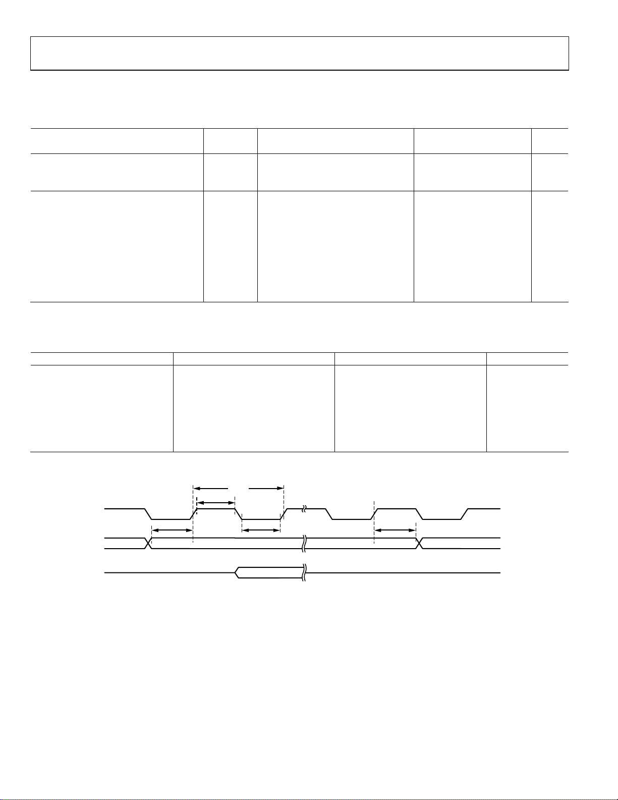
Table 3. Serial Data Port Timing Specifications
Parameter Description Min Max Unit
t
SCK high 50 ns
SCH
t
SCK low 50 ns
SCL
t
SCK period 312 ns
SCP
f
SCK
t
WS setup 0 ns
WSS
t
WS hold 20 ns
WSH
SCK frequency 0.5 3.2 MHz
fWS WS frequency 7.8 49.3 kHz
0.25 × VDD
V
TIMING DIAGRAM
SC
WS
SD
t
WSS
t
SCP
t
SCH
t
SCL
t
WSH
09568-103
Figure 3. Serial Data Port Timing
Rev. A | Page 4 of 16

Data Sheet ADMP441
A
E
A
ABSOLUTE MAXIMUM RATINGS
Table 4.
Parameter Rating
Supply Voltage (VDD) −0.3 V to +3.6 V
Sound Pressure Level 160 dB
Mechanical Shock 10,000 g
Vibration
Per MIL-STD-883 Method
2007, Test Condition B
Operating Temperature Range −40°C to +85°C
Digital Pin Input Voltage
−0.3 V to V
+ 0.3 V or 3.6 V,
DD
whichever is less
Stresses above those listed under Absolute Maximum Ratings
may cause permanent damage to the device. This is a stress
rating only; functional operation of the device at these or any
other conditions above those indicated in the operational
section of this specification is not implied. Exposure to absolute
maximum rating conditions for extended periods may affect
device reliability.
ESD CAUTION
LZON
CRITIC
TLTO T
P
t
L
09568-002
T
T
TURE
TEMPER
t
P
L
T
SMAX
T
SMIN
PREHEAT
t
25°C
t
S
RAMP-UP
TO PEAK
P
RAMP-DOWN
TIME
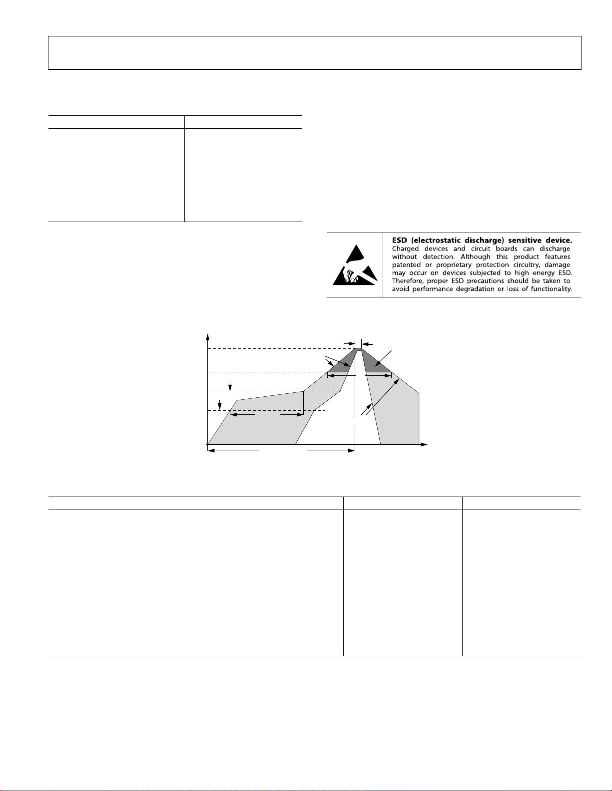
Figure 4. Recommended Soldering Profile Limits
Table 5. Recommended Soldering Profile Limits
Profile Feature Sn63/Pb37 Pb-Free
Average Ramp Rate (TL to TP) 1.25°C/sec max 1.25°C/sec max
Preheat
Minimum Temperature (T
Maximum Temperature (T
Time (T
Ramp-Up Rate (T
SMIN
to T
), tS 60 sec to 75 sec 60 sec to 75 sec
SMAX
to TL) 1.25°C/sec 1.25°C/sec
SMAX
) 100°C 100°C
SMIN
) 150°C 200°C
SMAX
Time Maintained Above Liquidous (tL) 45 sec to 75 sec ~50 sec
Liquidous Temperature (TL) 183°C 217°C
Peak Temperature (TP) 215°C +3°C/−3°C 260°C +0°C/−5°C
Time Within 5°C of Actual Peak Temperature (tP) 20 sec to 30 sec 20 sec to 30 sec
Ramp-Down Rate 3°C/sec max 3°C/sec max
Time 25°C (t
) to Peak Temperature 5 minute max 5 minute max
25°C
Rev. A | Page 5 of 16
 Loading...