Analog Devices ADMCF340 a (2) Datasheet
A
a
DashDSP® 64-Lead Flash and ROM Memory
Mixed-Signal DSP with Enhanced Analog Front End
ADMC(F)340
TARGET APPLICATIONS
Refrigerator and Air Conditioner Compressors,
Washing Machines
Industrial Variable Speed Drives, HVAC
MOTOR TYPES
Permanent Magnet Synchronous Motors (PMSM),
Brushless DC Motors (BDCM), AC Induction Motors
(ACIM), Switched Reluctance Motors (SRM)
FEATURES
20 MHz Fixed-Point DSP Core
Single Cycle Instruction Execution (50 ns)
ADSP-21xx Family Code Compatibility
Independent Computational Units
ALU
Multiplier/Accumulator
Barrel Shifter
Multifunction Instructions
Single Cycle Context Switch
Powerful Program Sequencer
Zero Overhead Looping
Conditional Instruction Execution
2 Independent Data Address Generators
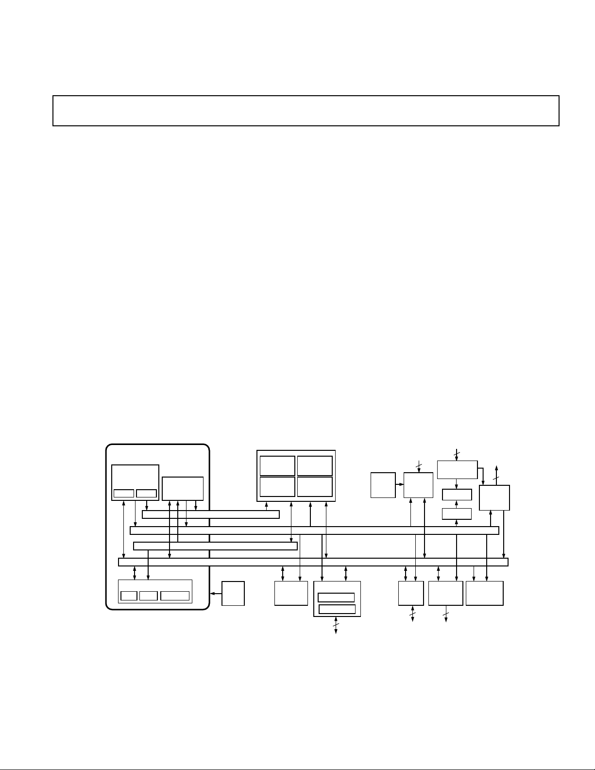
FUNCTIONAL BLOCK DIAGRAM
ADSP-21xx BASE
ARCHITECTURE
DATA
ADDRESS
GENERATORS
DAG 1 DAG 2
PROGRAM
SEQUENCER
PROGRAM MEMORY ADDRESS
DATA MEMORY ADDRESS
PROGRAM MEMORY DATA
DATA MEMORY DATA
MEMORY BLOCK
PROGRAM
ROM
4K 24
PROGRAM
RAM
512 24
Memory Configuration
512 16-Bit Data Memory RAM
512 24-Bit Program Memory RAM
4K 24-Bit Program Memory ROM
4K 24-Bit Total Program FLASH Memory
(ADMCF340 only)
3 Independent FLASH Memory Sectors
3584 24 Bit, 256 24 Bit, 256 24 Bit
Low Cost Pin Compatible ROM Option
16-Bit Watchdog Timer
Programmable 16-Bit Internal Timer with Prescaler
2 Double Buffered Serial Ports with SPI Mode
Support
Integrated Power-On Reset Function
3-Phase 16-Bit PWM Generation Unit
16-Bit Center-Based PWM Generator
Programmable PWM Pulsewidth
Edge Resolution of 50 ns
Programmable Narrow Pulse Deletion
153 Hz Minimum Switching Frequency
Double/Single Update Mode Control
Individual Enable and Disable for Each PWM
Output
High Frequency Chopping Mode for
Transformer-Coupled Gate Drives
(continued on page 8)
MOTOR CONTROL PERIPHERALS
PROGRAM
FLASH
4K 24
DATA
MEMORY
512 16
ADC SUBSYSTEM
V
ANALOG
REF
2.5V
INPUTS
10
I
SENSE
AND TRIP
SHA
TIMERS
3
AMP
16-BIT
THREE-
PHASE
PWM
6
ARITHMETIC UNITS
SHIFTER
MACALU
DashDSP is a registered trademark of Analog Devices, Inc.
POR
TIMER
REV. A
Information furnished by Analog Devices is believed to be accurate and
reliable. However, no responsibility is assumed by Analog Devices for its
use, nor for any infringements of patents or other rights of third parties that
may result from its use. No license is granted by implication or otherwise
under any patent or patent rights of Analog Devices.
SERIAL PORT
SPORT 0
SPORT 1
7
One Technology Way, P.O. Box 9106, Norwood, MA 02062-9106, U.S.A.
Tel: 781/329-4700 www.analog.com
Fax: 781/326-8703 © Analog Devices, Inc., 2002
PIO
2 16-BIT
AUX
PWM
225
WATCH-
DOG
TIMER

ADMC(F)340
(VDD = 5%, GND = 0 V. For ADMCF340, TA = –40C to +85C.
ANALOG-TO-DIGITAL CONVERTER
Parameter Min Typ Max Unit Conditions/Comments
Signal Input 0.3 3.5 V VAUX0, VAUX1, VAUX2
Resolution
Linearity Error
Zero Offset
Comparator Delay 600 ns
ADC High Level Input Current
ADC Low Level Input Current
NOTES
1
Resolution varies with PWM switching frequency (double update mode) 78.1 kHz = 8 bits, 4.9 kHz = 12 bits.
2
2.44 kHz sample frequency, VAUX0, VAUX1, VAUX2.
3
Extrapolated point outside of operating range. 2.44 kHz sample frequency.
Specifications subject to change without notice.
1
2
3
2
2
–32 0 +7 mV
–10 µAV
For ADMC340, TA = –40C to +125C. CLKIN = 10 MHz, unless otherwise noted.)
12 Bits
3 4 Bits
10 µAV
= 3.5 V
IN
= 0.0 V
IN
I
AMPLIFIER–TRIP
SENSE
Parameter Min Typ Max Unit Conditions/Comments
Signal Operating Range –400 +400 mV
I
SENSE
I
Gain –2.6 –2.51 –2.34 % VIN = –400 mV to +400 mV
SENSE
Gain Channel Matching 5.5 % VIN = –400 mV to +400 mV
I
SENSE
I
Gain Stability
SENSE
I
Linearity
SENSE
Internal Offset Voltage
I
SENSE
I
Internal Offset Stability
SENSE
I
Signal-to-Noise Ratio (SNR)
SENSE
Signal-to-Noise Ratio Less Distortion 54 dB
I
SENSE
3
(SNR)
I
Total Harmonic Distortion
SENSE
Input Current –200 +10 µAV
I
SENSE
I
Input Resistance 11.5 kΩ
SENSE
1
2
2
2
3
3
89 Bits
1.68 1.87 2.1 V
0.8 % VIN = –400 mV to +400 mV
2.1 %
51 dB
–40 dB
–53 dB
= –400 mV to +400 mV
IN
TRIP Threshold Low –690 –430 mV
TRIP Threshold High +430 +690 mV
TRIP Minimum Pulsewidth
NOTES
1
Variation of gain with VDD and temperature.
2
VIN = –400 mV to +400 mV.
3
fIN = 1 kHz sine wave, VIN = –400 mV to +400 mV, fS = 4 kHz.
4
High or low TRIP threshold.
Specifications subject to change without notice.
CURRENT SOURCE
4
5 µs
1
Parameter Min Typ Max Unit Conditions/Comments
Programming Resolution 3 Bits
Tuned Current
NOTES
1
For ADC calibration.
2
0.3 V to 3.5 V I
Specifications subject to change without notice.
2
CONST
91 100 109 µA
voltage.
–2–
REV. A

ADMC(F)340
VOLTAGE REFERENCE
Parameter Min Typ Max Unit Conditions/Comments
Voltage Level (V
)2.44 2.50 2.55 V –40°C to +85°C (ADMCF340 only)
REF
2.44 2.50 2.55 V –40°C to +125°C (ADMC340 ROM only)
Drift 110 ppm/°C
Specifications subject to change without notice.
POWER-ON RESET
Parameter Min Typ Max Unit Conditions/Comments
Reset Threshold 3.20 3.65 4.10 V
Hysteresis 100 mV
Reset Active Timeout Period 3.2
*216 CLKOUT cycles.
Specifications subject to change without notice.
*
ms
ELECTRICAL CHARACTERISTICS
Symbol Parameter Min Typ Max Unit Conditions/Comments
V
IL
V
IH
V
IL
V
IH
V
OL
V
OL
V
OH
I
IL
I
IL
I
IH
I
IH
I
IH
I
OZH
I
OZL
I
DD
I
DD
I
DD
I
DD
NOTES
1
PWMPOL and PWMSR pins only.
2
Output pins PORTA0–PORTA8, PORTB0–PORTB15, AH, AL, BH, BL, CH, CL.
3
XTAL pin.
4
Internal pull-up, RESET.
5
Internal pull-down, PWMTRIP, PORTA0–PORTA8, PORTB0–PORTB15.
6
Three-stateable pins, DT1, RFS0, TFS0, SCLK1.
7
Outputs not switching.
Specifications subject to change without notice.
Low Level Input Voltage 0.8 V
High Level Input Voltage 2 V
Low Level Input Voltage
High Level Input Voltage 2.60 V
Low Level Output Voltage
Low Level Output Voltage
High Level Output Voltage 4 V I
Low Level Input Current RESET Pin
Low Level Input Current –10 µAV
High Level Input Current RESET Pin
High Level Input Current
High Level Input Current 10 µAV
High Level Three-State Leakage Current
Low Level Three-State Leakage Current6–10 µAV
Supply Current (Idle)
Supply Current (Dynamic)
Supply Current (Idle)
Supply Current (Dynamic)
1
2
3
4
4
5
7
7
7
7
–100 µAV
6
1.75 V
0.4 V I
0.8 V I
30 µAV
100 µAV
100 µAV
2 mA
OL =
= 2 mA
OL
= 0.5 mA
OH
= 0 V
IN
= 0 V
IN
= V
IN
= V
IN
= V
IN
= V
IN
= 0 V
IN
DD
DD
DD
DD
35 mA VDD = 5.25 V (ADMC340 only)
60 mA VDD = 5.25 V (ADMC340 only)
55 mA VDD = 5.25 V (ADMCF340 only)
135 mA VDD = 5.25 V (ADMCF340 only)
REV. A
–3–
ADMC(F)340
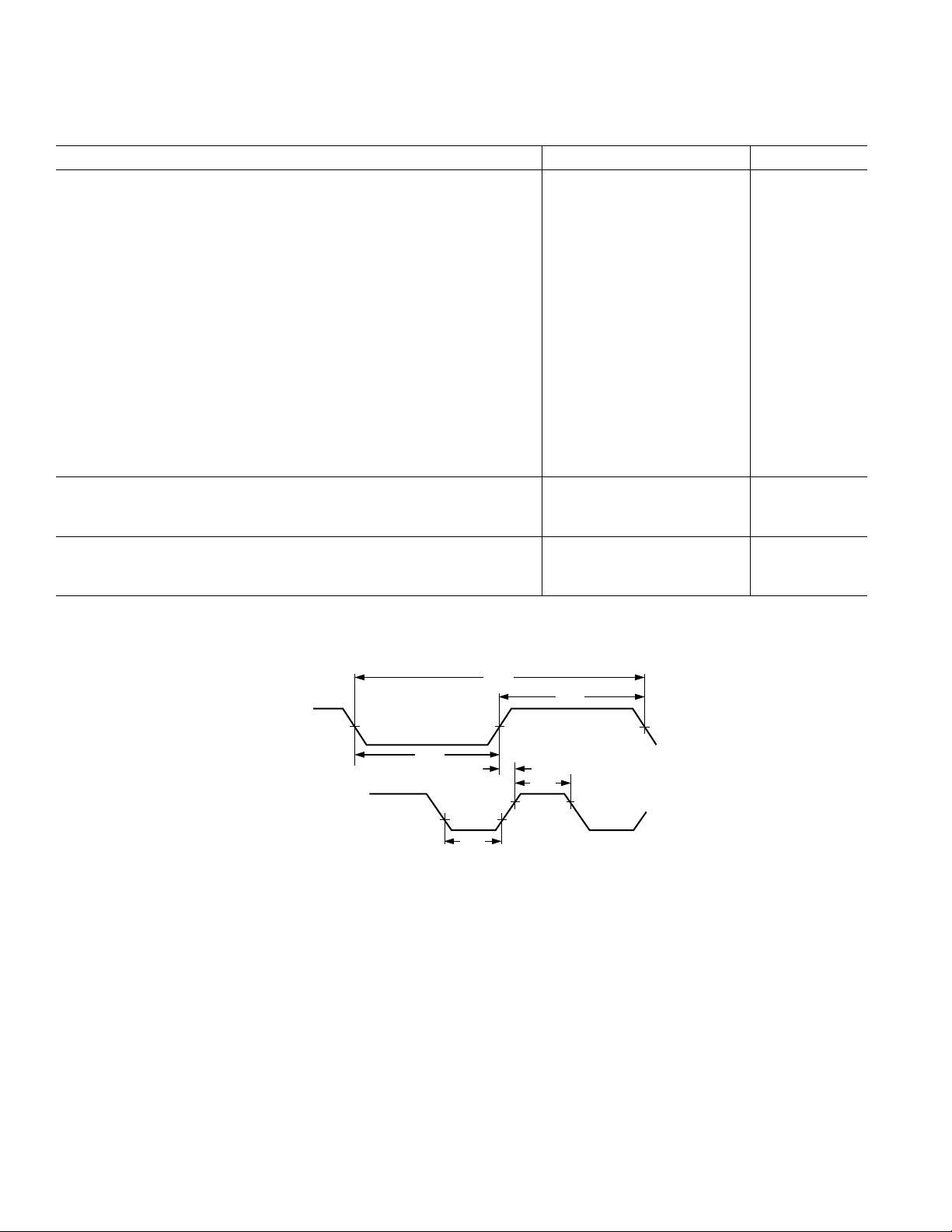
TIMING PARAMETERS
Parameter Min Max Unit
Clock Signals
Signal TCK is defined as 0.5 t
a frequency equal to half the instruction rate; a 10 MHz input clock (which is
equivalent to 100 ns) yields a 50 ns processor cycle (equivalent to 20 MHz).
When T
values are within the range of 0.5 t
CK
substituted for all relevant timing parameters to obtain specification value as
in the following example:
t T ns ns ns ns
=−=×−=05 10 05 50 10 15..
CKH CK
Timing Requirements:
t
CKIN
t
CKIL
t
CKIH
CLKIN Period 100 150 ns
CLKIN Width Low 20 ns
CLKIN Width High 20 ns
Switching Characteristics:
t
CKL
t
CKH
t
CKOH
CLKOUT Width Low 0.5 TCK – 10 ns
CLKOUT Width High 0.5 TCK – 10 ns
CLKIN High to CLKOUT High 0 20 ns
Control Signals
Timing Requirement:
t
RSP
RESET Width Low 5 TCK* ns
PWM Shutdown Signals
Timing Requirement:
t
PWMTPW
*Applies after power-up sequence is complete.
Specifications subject to change without notice.
PWMTRIP Width Low T
. The ADMC(F)340 uses an input clock with
CKIN
period, they should be
CKIN
CK
ns
CLKIN
CLKOUT
t
CKIN
t
CKIL
t
CKL
Figure 1. Clock Signals
t
t
CKOH
CKH
t
CKIH
–4–
REV. A
ADMC(F)340
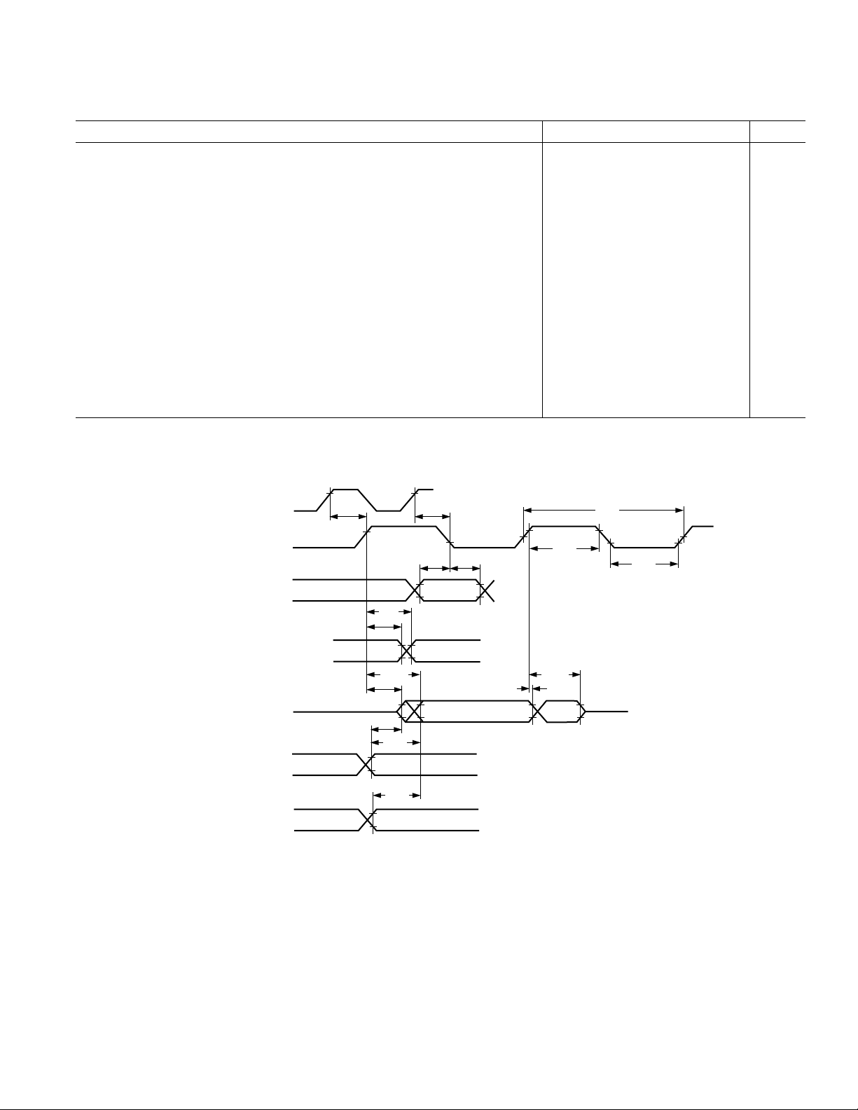
TIMING PARAMETERS
Parameter Min Max Unit
Serial Ports
Timing Requirements:
t
SCK
t
SCS
t
SCH
t
SCP
Switching Characteristics:
t
CC
t
SCDE
t
SCDV
t
RH
t
RD
t
SCDH
t
SCDD
t
TDE
t
TDV
t
RDV
Specifications subject to change without notice.
SCLK Period 100 ns
DR/TFS/RFS Setup before SCLK Low 15 ns
DR/TFS/RFS Hold after SCLK Low 20 ns
SCLKIN Width 40 ns
CLKOUT High to SCLK
OUT
0.25 T
0.25 TCK + 20 ns
CK
SCLK High to DT Enable 0 ns
SCLK High to DT Valid 30 ns
TFS/RFS
TFS/RFS
Hold after SCLK High 0 ns
OUT
Delay from SCLK High 30 ns
OUT
DT Hold after SCLK High 0 ns
SCLK High to DT Disable 30 ns
TFS (Alt) to DT Enable 0 ns
TFS (Alt) to DT Valid 25 ns
RFS (Multichannel, Frame Delay Zero) to DT Valid 30 ns
CLKOUT
SCLK
DR
RFS
TFS
RFS
OUT
TFS
OUT
DT
TFS
(ALTERNATE
FRAME MODE)
(MULTICHANNEL MODE,
FRAME DELAY 0 [MFD = 0])
RFS
t
CC
IN
IN
t
t
SCDE
t
TDE
t
RH
t
RD
SCDV
t
TDV
t
RDV
t
CC
t
SCDD
t
t
t
SCS
SCH
t
SCDH
SCP
t
SCK
t
SCP
Figure 2. Serial Port Timing
REV. A
–5–

ADMC(F)340
WARNING!
ESD SENSITIVE DEVICE
ABSOLUTE MAXIMUM RATINGS*
Supply Voltage (VDD) . . . . . . . . . . . . . . . . . . –0.3 V to +7.0 V
Supply Voltage (AV
Input Voltage . . . . . . . . . . . . . . . . . . . . –0.3 V to V
Output Voltage Swing . . . . . . . . . . . . . –0.3 V to V
) . . . . . . . . . . . . . . . . . –0.3 V to +7.0 V
DD
+ 0.3 V
DD
+ 0.3 V
DD
ADMC340 Operating Temperature
Range (Ambient) . . . . . . . . . . . . . . . . . . . . –40°C to +85°C
ADMC340 Operating Temperature
Range . . . . . . . . . . . . . . . . . . . . . . . . . . . . –40°C to +125°C
Storage Temperature Range . . . . . . . . . . . . –65°C to +150°C
Lead Temperature (5 sec) . . . . . . . . . . . . . . . . . . . . . . . 280°C
*Stresses greater than those listed may cause permanent damage to the device.
These are stress ratings only; functional operation of the device at these or any
other conditions greater than those indicated in the operational sections of this
specification is not implied. Exposure to absolute maximum rating conditions for
extended periods may affect device reliability.
1
AGND
2
DGND1
3
RESET
4
PB6
5
CH
6
PB7
7
PB8
8
CL
9
PB9
10
PB10
11
BH
12
PB11
13
PB12
14
BL
15
NC
16
NC
NC = NO CONNECT
PIN CONFIGURATION
NC
ICONST
VAUX7
VAUX2
VAUX6
VAUX1
VAUX5
VAUX0
61
59
60
ADMC(F)340
20
22
21
PB14ALPB15
58
57
56
TOP VIEW
(Not to Scale)
23
24
25
PA8/(AUX0/CLKOUT)
PA7/(AUX1/PWMSYNC)
63
64
PIN 1
IDENTIFIER
18
17
NC
AH
62
19
PB13
SENSE1
VAUX4
I
55
26
2
DD
DV
PWMSR
V1
54
27
DGND2
53
28
SENSE2
SENSE3
I
V2
I
V3
50
52
51
31
29
30
PA6/DR1
PWMPOL
PA5/(FL1/DT1)
PA4(SCLK1/SCLK0)
PWMTRIP
49
48
47
46
45
44
43
42
41
40
39
38
37
36
35
34
33
32
PA3/TFS0
AV
DD
DVDD1
XTAL
NC
CLKIN
NC
PB5
PB4
PA0/DR0
PB3
PB2
PA1/DT0
PB1
PB0
PA2/RFS0
NC
ORDERING GUIDE
Temperature Instruction Package Package
Model Range Rate Description Option
ADMC(F)340BST –40°C to +85°C 20 MHz 64-Lead Thin Plastic Quad Flatpack ST-64
(LQFP)
ADMC(F)340-EVALKIT N/A N/A Development Tool Kit
ADMC340VST-XXX-XXXX –40°C to +125°C 20 MHz 64-Lead LQFP ST-64
CAUTION
ESD (electrostatic discharge) sensitive device. Electrostatic charges as high as 4000 V readily
accumulate on the human body and test equipment and can discharge without detection. Although
the ADMC(F)340 features proprietary ESD protection circuitry, permanent damage may occur on
devices subjected to high energy electrostatic discharges. Therefore, proper ESD precautions are
recommended to avoid performance degradation or loss of functionality.
–6–
REV. A

PIN FUNCTION DESCRIPTIONS
ADMC(F)340
Pin Pin
No. Mnemonic Type
1 AGND GND
2 DGND1 GND
3 RESET D_IN
4 PB6 D_I/O
5CH D_OUT
6 PB7 D_I/O
7 PB8 D_I/O
8CL D_OUT
9 PB9 D_I/O
10 PB10 D_I/O
11 BH D_OUT
12 PB11 D_I/O
13 PB12 D_I/O
14 BL D_OUT
15 NC No Connect
16 NC No Connect
17 NC No Connect
18 AH D_OUT
19 PB13 D_I/O
20 PB14 D_I/O
21 AL D_OUT
22 PB15 D_I/O
23 PA8/(AUX0/CLKOUT) D_I/O
24 PA7/(AUX1/PWMSYNC) D_I/O
25 DV
2SUP
DD
26 PWMSR D_IN
27 DGND2 GND
28 PA6/DR1 D_I/O
29 PA5/(FL1/DT1) D_I/O
30 PA4/(SCLK1/SCLK0) D_I/O
31 PWMPOL D-IN
32 PA3/TFS0 D_I/O
Pin Pin
No. Mnemonic Type
33 NC No Connect
34 PA2/RFS0 D_I/O
35 PB0 D_I/O
36 PB1 D_I/O
37 PA1/DT0 D_I/O
38 PB2 D_I/O
39 PB3 D_I/O
40 PA0/DR0 D_I/O
41 PB4 D_I/O
42 PB5 D_I/O
43 NC No Connect
44 CLKIN D_I/O
45 NC No Connect
46 XTAL A_OUT
47 DV
48 AV
1SUP
DD
DD
SUP
49 PWMTRIP D_IN
50 V3 A_IN
51 I
SENSE3
A_IN
52 V2 A_IN
53 I
SENSE2
A_IN
54 V1 A_IN
55 I
SENSE1
A_IN
56 VAUX4 A_IN
57 VAUX0 A_IN
58 VAUX5 A_IN
59 VAUX1 A_IN
60 VAUX6 A_IN
61 VAUX2 A_IN
62 VAUX7 A-IN
63 ICONST A_OUT
64 NC No Connect
PA is the abbreviation of PORTA; PB is the abbreviation of PORTB.
REV. A
–7–
ADMC(F)340
(continued from page 1)
External PWMTRIP Pin
Switched Reluctance Motor Mode Selection Pin
PWM Polarity Selection Pin
Integrated 13-Channel ADC Subsystem
3 Bipolar I
Inputs with Programmable
SENSE
Sample-and-Hold Amplifier and Overcurrent
Protection (Usable as 3 Dedicated Analog Inputs)
3 Simultaneous Converting Voltage Inputs
7 Muxed Auxiliary Analog Inputs
Internal Voltage Reference (2.5 V)
Acquisition Synchronized to PWM Switching
Frequency
25-Lead Digital I/O Port
Bit Configurable as Input or Output
Change of State Interrupt Support
2 16-Bit Auxiliary PWM Timers
Synthesized Analog Output
Programmable Frequency
0% to 100% Duty Cycle
2 Programmable Operation Modes
Independent Mode/Offset Mode
GENERAL DESCRIPTION
The ADMC(F)340 is a low cost, single-chip DSP-based
controller suitable for permanent magnet synchronous, ac
induction, switched reluctance, and brushless dc motors. The
ADMC(F)340 integrates a 20 MHz, fixed-point DSP core with
a complete set of motor control and system peripherals for fast,
efficient development of motor controllers.
The DSP core of the ADMC(F)340 is completely code compatible
with the ADSP-21xx DSP family and combines three computational units, data address generators, and a program sequencer.
The computational units comprise an ALU, a multiplier/accumulator (MAC), and a barrel shifter. There are special instructions
for bit manipulation, multiplication (x squared), biased rounding,
and global interrupt masking. The system peripherals are the
power-on reset circuit (POR), the watchdog timer, and two
synchronous serial ports. The serial ports are configurable
and double buffered, with hardware support for UART, SCI,
and SPI port emulation. The ADMC(F)340 provides 512 × 24-bit
program memory RAM, 4K × 24-bit program memory ROM,
4K × 24-bit program FLASH memory, and 512 × 16-bit data
memory RAM. The user code will be stored and executed from
the flash memory. The program and data memory RAM can be
used for dynamic data storage or can be loaded through the
serial port from an external device as in other ADMCxx family
parts. The program memory ROM contains a monitor function
as well as useful routines for erasing, programming, and verifying
the flash memory.
The motor control peripherals of the ADMC(F)340 provide a 12-bit
analog data acquisition system with 13 analog input channels,
three dedicated I
functions (combining internal amplifi-
SENSE
cation, sampling, and overcurrent PWM shutdown features),
and an internal voltage reference. In addition, a three-phase,
16-bit, center-based PWM generation unit can be used to produce
high accuracy PWM signals with minimal processor overhead. The
ADMC(F)340 also contains two 16-bit auxiliary PWM timers
and 25 lines of programmable digital I/O.
Several functions, such as the auxiliary PWM and the serial
communication ports, are multiplexed with the nine PORTA
(9, PIO) programmable input/output (PIO) pins. The other 16
programmable digital I/O pins are dedicated. The pin functions
can be independently selected to allow maximum flexibility
for different applications.
DATA
ADDRESS
GENERATOR
No. 1
INPUT REGS
ALU
OUTPUT REGS
DATA
ADDRESS
GENERATOR
No. 2
INPUT REGS
OUTPUT REGS
MAC
INSTRUCTION
REGISTER
PM ROM
4K 24
PROGRAM
SEQUENCER
16
R BUS
14
14
24
BUS
EXCHANGE
16
INPUT REGS
SHIFTER
OUTPUT REGS
PM RAM
512 24
CONTROL
LOGIC
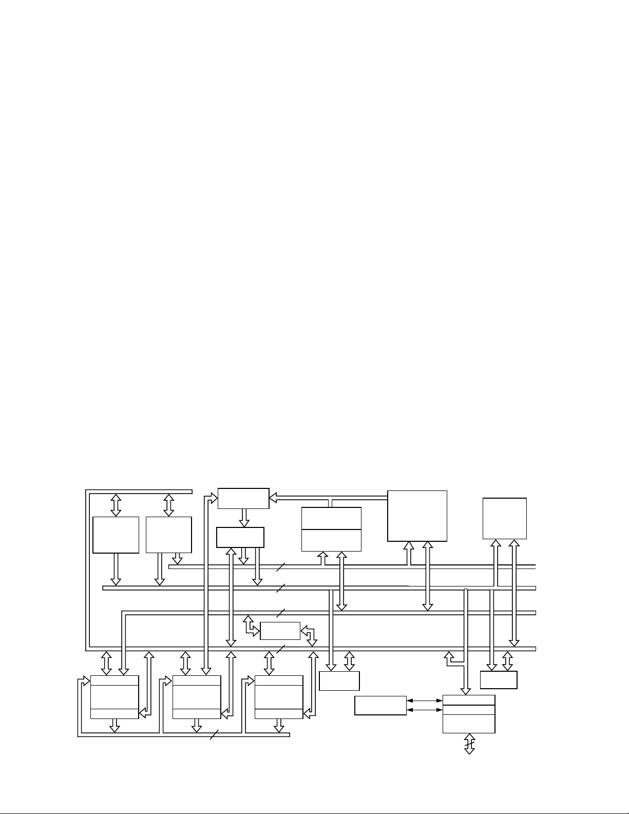
Figure 3. DSP Core Block Diagram
–8–
PMA BUS
DMA BUS
PMD BUS
DMD BUS
COMPANDING
CIRCUITRY
FLASH
PROGRAM
MEMORY
4K 24
TRANSMIT REG
RECEIVE REG
SERIAL
PORT
6
DM RAM
512 16
TIMER
REV. A

ADMC(F)340
DSP CORE ARCHITECTURE OVERVIEW
Figure 3 is an overall block diagram of the DSP core of the
ADMC(F)340. The flexible architecture and comprehensive
instruction set allow the processor to perform multiple operations
in parallel. In one processor cycle (50 ns with a 10 MHz CLKIN),
the DSP core can:
• Generate the next program address
• Fetch the next instruction
• Perform one or two data moves
• Update one or two data address pointers
• Perform a computational operation
This all takes place while the processor continues to:
•
Receive and transmit through the serial ports
•
Decrement the interval timer
•
Generate three-phase PWM waveforms for a power inverter
•
Generate two signals using the 16-bit auxiliary PWM timers
•
Acquire four analog signals
•
Decrement the watchdog timer
The processor contains three independent computational units:
the arithmetic and logic unit (ALU), the multiplier/accumulator
(MAC), and the shifter. The computational units process 16-bit
data directly and have provisions to support multiprecision com-
putations. The ALU performs a standard set of arithmetic and
logic operations as well as provides support for division primitives.
The MAC performs single-cycle multiply, multiply/add, and
multiply/subtract operations with 40 bits of accumulation. The
shifter performs logical and arithmetic shifts, normalization,
denormalization, and derive-exponent operations. The shifter
can be used to efficiently implement numeric format control,
including floating-point representations. The internal result (R)
bus directly connects the computational units so that the output
of any unit may be the input of any unit on the next cycle.
A powerful program sequencer and two dedicated data address
generators ensure efficient delivery of operands to these compu-
tational units. The sequencer supports conditional jumps and
subroutine calls and returns in a single cycle. With internal loop
counters and loop stacks, the ADMC(F)340 executes looped code
with zero overhead; no explicit jump instructions are required to
maintain the loop.
Two data address generators (DAGs) provide addresses for
simultaneous dual operand fetches from data memory and pro-
gram memory. Each DAG maintains and updates four address
pointers (I registers). Whenever the pointer is used to access
data (indirect addressing), it is post-modified by the value in
one of four modify (M) registers. A length value may be associated
with each pointer (L registers) to implement automatic modulo
addressing for circular buffers. The circular buffering feature is also
used by the serial ports for automatic data transfers to and from
on-chip memory. DAG1 generates only data memory addresses and
provides an optional bit-reversal capability. DAG2 may generate
either program or data memory addresses but has no bit-reversal
capability. Efficient data transfer is achieved with the use of five
internal buses:
• Program memory address (PMA) bus
• Program memory data (PMD) bus
• Data memory address (DMA) bus
• Data memory data (DMD) bus
• Result (R) bus
REV. A
–9–
Program memory can store both instructions and data, permitting
the ADMC(F)340 to fetch two operands in a single cycle—one from
program memory and one from data memory. The ADMC(F)340
can fetch both an operand from on-chip program memory and the
next instruction in the same cycle. The ADMC(F)340 writes
data from its 16-bit registers to the 24-bit program memory by
using the PX Register to provide the lower eight bits. When it reads
data (not instructions) from 24-bit program memory to a 16-bit
data register, the lower eight bits are placed into the PX Register.
The ADMC(F)340 can respond to a number of distinct DSP core
and peripheral interrupts. The DSP interrupts comprise a serial port
receive interrupt, a serial port transmit interrupt, a timer interrupt, and two software interrupts. Additionally, the motor control
peripherals include two PWM interrupts and a PIO interrupt.
The serial port (SPORT0) provides a complete synchronous
serial interface with optional companding in hardware and a wide
variety of framed and unframed data transmit and receive modes of
operation. SPORT0 and SPORT1 can generate an internal
programmable serial clock or accept an external serial clock.
A programmable interval counter is also included in the DSP core
and can be used to generate periodic interrupts. A 16-bit count
register (TCOUNT) is decremented every n processor cycle,
where n – 1 is a scaling value stored in the 8-bit TSCALE Register.
When the value of the counter reaches zero, an interrupt is
generated and the count register is reloaded from a 16-bit period
register (TPERIOD).
The ADMC(F)340 instruction set provides flexible data moves
and multifunction (one or two data moves with a computation)
instructions. Each instruction is executed in a single 50 ns
processor cycle (for a 10 MHz CLKIN). The ADMC(F)340
assembly language uses an algebraic syntax for ease of coding
and readability. A comprehensive set of development tools
supports program development. For further information on the
DSP core, refer to the ADSP-2100 Family User’s Manual, Third
Edition, with particular reference to the ADSP-2171.
SERIAL PORTS
The ADMC(F)340 incorporates two synchronous serial ports
(SPORT1 and SPORT0) for serial communication and multiprocessor communication. SPORT1 is primarily intended for
the interfacing of the debugging tools and/or code booting from
an external serial memory.
The following is a brief list of capabilities of the ADMC(F)340
SPORTs:
• SPORTs are bidirectional and have a separate, doublebuffered transmit and receive section.
• SPORTs can use an external serial clock or generate their
own serial clock internally.
• SPORTs have independent framing for the receive and
transmit sections. Sections run in a frameless mode or with
frame synchronization signals internally or externally
generated. Frame synchronization signals are active high or
inverted, with either of two pulsewidths and timings.
• SPORTs support serial data-word lengths from three bits to
16 bits and provide optional A-law and µ-law companding
according to ITU (formerly CCITT) recommendation G.711.
• SPORTs’ receive and transmit sections can generate unique
interrupts on completing a data-word transfer.
• SPORTs can receive and transmit an entire circular buffer
of data with only one overhead cycle per data-word. An
interrupt is generated after a data buffer transfer.

ADMC(F)340
• SPORT0 has one pin, SCLK0, shared with SPORT1.
During a boot phase (SPORT1 Boot Mode enabled by a bit
in the MODECTRL Register), the serial clock of SPORT1 is
externally available. The serial clock of SPORT0 is externally
available when the SPORT1 is configured in UART Mode.
• SPORT0 can be configured as a SPI Port (master mode only).
Refer to Table XI for more information. The clock phase and
polarity are programmable through the MODECTRL Register.
Refer to Table XI for pin configuration.
• SPORT0 has a multichannel interface to selectively receive
and transmit a 24-word or 32-word time division multiplexed
serial bit stream.
• SPORT1 is the default port for program/data memory boot
loading and for the development tools interface. The DT1/FL1
pin can be configured as the SROM/E
2
PROM reset signal.
The ADMC(F)340 is available in a 64-lead LQFP package.
PIN FUNCTION DESCRIPTION
Table I. Pin List
Pin Group No. of Input/
Name Pins Output Function
PWMPOL 1 I PWM Polarity
PWMSR 1I PWM Switched
Reluctance Mode
RESET 1I Processor Reset Input
SPORT1
SPORT0
1
1
2 I/O Serial Port 1 Pins
(DT1/FL1, DR1)
5 I/O Serial Port 0 Pins
(DT0, DR0, RFS0,
CLKOUT
TFS0, SCLK1/
1
1
1
I/O Processor Clock
SCLK0
2
)
Output
CLKIN, XTAL 2 I/O External Clock or
Quartz Crystal
1
PORTA0–PORTA8
PORTB0–PORTB15 16 I/O Digital I/O Port Pins
AUX0–AUX1
1
9 I/O Digital I/O Port Pins
2O Auxiliary PWM
Connection Point
Outputs
AH-CL 6 O PWM Outputs
PWMTRIP 1I PWM Trip Signal
V1 to V3 3 I I
I
SENSE1 to ISENSE3
3I Analog Inputs
SENSE
Inputs
VAUX0-VAUX7 7 I Auxiliary Analog Inputs
ICONST 1 O ADC Constant
Current Source
DV
AV
DD
DD
3I Power Supply
3I Power Supply
GND 3 I Ground
NOTES
1
Multiplexed pins, individually selectable through PORTA_SELECT and
PORTA_DATA Registers.
2
SCLK1/SCLK0 multiplexed signals, selectable through MODECTRL
Register Bit 4.
INTERRUPT OVERVIEW
The ADMC(F)340 can respond to 34 different interrupt sources
with minimal overhead, seven of which are internal DSP core
interrupts and 27 of which are from the motor control peripherals.
The seven DSP core interrupts are SPORT1 receive (or IRQ0)
and transmit (or IRQ1), SPORT0 receive and transmit, the
internal timer, and two software interrupts. The motor control
peripheral interrupts are the 25 programmable I/Os and two from
the PWM (PWMSYNC pulse and PWMTRIP). All motor control
interrupts are multiplexed into the DSP core through the peripheral IRQ2 interrupt. The interrupts are internally prioritized and
individually maskable. A detailed description of the entire interrupt
system of the ADMC(F)340 is presented in the Interrupt
Control section, which follows the detailed descriptions of each
peripheral block.
MEMORY MAP
The ADMC(F)340 has two distinct memory types: program
and data. In general, program memory contains user code and
coefficients, while the data memory is used to store variables and
data during program execution. Three kinds of program memory are
provided on the ADMC(F)340: RAM, ROM, and FLASH. The
motor control peripherals are memory mapped into a region of the
data memory space starting at 0x2000. The complete program and
data memory maps are given in Tables II and III, respectively.
Table II. Program Memory Map
Memory
Address Range Type Function
0x0000–0x002F RAM Internal Vector Table
0x0030–0x01FF RAM User Program Memory
0x0200–0x07FF Reserved
0x0800–0x17FF ROM Reserved Program Memory
0x1800–0x1FFF Reserved
0x2000–0x20FF FLASH User Program Memory
Sector 0
0x2100–0x21FF FLASH User Program Memory
Sector 1
0x2200–0x2FFF FLASH User Program Memory
Sector 2
0x3000–0x3FFF Reserved
Table III. Data Memory Map
Memory
Address Range Type Function
0x0000–0x1FFF Reserved
0x2000–0x20FF Memory Mapped Registers
0x2100–0x37FF Reserved
0x3800–0x39FF RAM User Data Memory
0x3A00–0x3BFF RAM Reserved
0x3C00–0x3FFF Memory Mapped Registers
–10–
REV. A
ADMC(F)340
FLASH MEMORY SUBSYSTEM
The ADMC(F)340 has 4K × 24-bit user-programmable, nonvolatile flash memory. A flash programming utility is provided with the
development tools and performs the basic device programming
operations: erase, program, and verify.
The flash memory array is portioned into three asymmetrically
sized sectors of 256 words, 256 words, and 3,584 words, labeled
Sector 0, Sector 1, and Sector 2, respectively. These sectors are
mapped into external program memory address space.
Four flash memory interface registers are connected to the DSP.
These 16-bit registers are mapped into the register area of data
memory space. They are named Flash Memory Control Register
(FMCR), Flash Memory Address Register (FMAR), Flash
Memory Data Register Low (FMDRL), and Flash Memory Data
Register High (FMDRH). These registers are diagrammed
beginning with Figure 21. They are used by the flash memory
programming utility. The user program may read these registers
but should not modify them directly. The flash programming
utility provides a complete interface to the flash memory.
Note that from the point of view of 2171 core, the flash memory
is placed externally. It means the core accesses them through an
external memory interface that multiplexes the program memory
and data memory buses into a single external bus. Therefore, if
more than one external transfer must be made in the same
instruction, there will be at least one overhead cycle required.
Special Flash Registers
The flash module has four nonvolatile 8-bit registers called Special
Flash Registers (SFRs) that are accessible independently of
the main flash array via the flash programming utility. These
registers are for general-purpose, nonvolatile storage. When
erased, the Special Flash Registers contain all 0s. To read
Special Flash Registers from the user program, call the read_reg
routine contained in the ROM. Refer to the ADMCF34x DSP
Motor Controller Developers’ Reference Manual for an example.
Boot-from-Flash Code
A security feature is available in the form of a code that when set
causes the processor to execute the program in flash memory at
power-up or reset. In this mode, the flash programming utility and
debugger are unable to communicate with the ADMC(F)340.
Consequently, the contents of the flash memory can be neither
programmed nor read.
The boot-from-flash code may be set via the flash programming
utility when the user’s program is thoroughly tested and loaded
into flash program memory at Address 0x2200. The user’s program must contain a mechanism for clearing the boot-from-flash
code if reprogramming the flash memory is desired. The only
way to clear boot-from-flash is from within the user program, by
calling the flash_init or auto_erase_reg routines that are included
in the ROM. The user program must be signaled in some way to
call the necessary routine to clear the boot-from-flash code. An
example would be to detect a high level on a PIO pin during
startup initialization and then call the flash_init or auto-erase-reg
routine. The flash_init routine will erase the entire user program
in flash memory before clearing the boot-from-flash code, thus
ensuring the security of the user program. If security is not a
concern, the auto_erase_reg routine can be used to clear the
boot-from-flash code while leaving the user program intact.
Refer to the ADMCF34x DSP Motor Controller Developers’
Reference Manual for further instructions and an example of
using the boot-from-flash code.
FLASH PROGRAM BOOT SEQUENCE
On power-up or reset, the processor begins instruction execution
at Address 0x0800 of internal program ROM. The ROM monitor
program that is located there checks the boot-from-flash code. If
that code is set, the processor jumps to location 0x2200 in external
flash program memory, where it expects to find the user’s
application program.
If the boot-from-flash code is not set, the monitor attempts to
boot from an external device as described in the ADMCF34x
DSP Motor Controller Developers’ Reference Manual.
SYSTEM INTERFACE
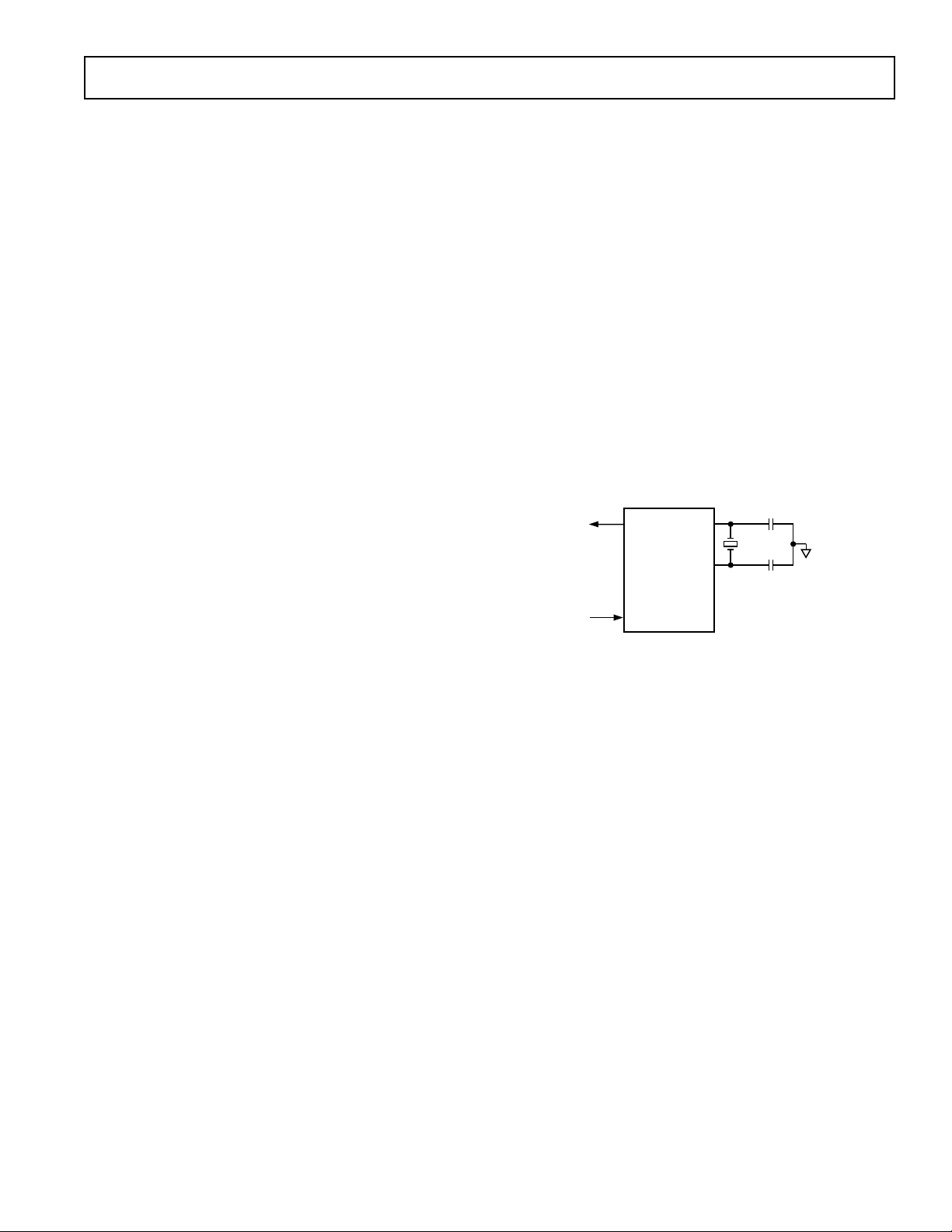
Figure 4 shows a basic system configuration for the ADMC(F)340
with an external crystal.
22pF
10MHz
22pF
Figure 4. Basic System Configuration
Clock Signals
CLKOUT
CLKIN
ADMC(F)340
RESET
XTAL
The ADMC(F)340 can be clocked either by a crystal or a TTL
compatible clock signal. For normal operation, the CLKIN
input cannot be halted, changed during operation, or operated
below the specified minimum frequency. If an external clock is
used, it should be a TTL compatible signal running at half the
instruction rate. The signal is connected to the CLKIN pin of
the ADMC(F)340. In this mode, with an external clock signal,
the XTAL pin must be left unconnected. The ADMC(F)340
uses an input clock with a frequency equal to half the instruction rate; a 10 MHz input clock yields a 50 ns processor cycle
(which is equivalent to 20 MHz). Normally, instructions are
executed in a single processor cycle. All device timing is relative to the internal instruction rate that is indicated by the
CLKOUT signal when enabled.
Because the ADMC(F)340 includes an on-chip oscillator feedback
circuit, an external crystal may be used instead of a clock source,
as shown in Figure 2. The crystal should be connected across the
CLKIN and XTAL pins with two capacitors (see Figure 2). A
parallel-resonant, fundamental frequency, microprocessor-grade
crystal should be used. A clock output signal (CLKOUT) is
generated by the processor at the processor’s cycle rate of twice
the input frequency.
REV. A
–11–
ADMC(F)340
Reset
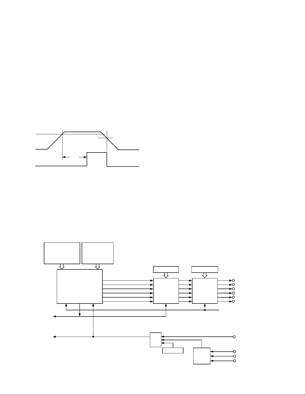
The ADMC(F)340 DSP core and peripherals must be correctly
reset when the device is powered up to ensure proper unitization.
The ADMC(F)340 contains an integrated power-on-reset (POR)
circuit that provides a complete system reset on power-up and
power-down. The POR circuit monitors the voltage on the
ADMC(F)340 V
in reset while V
When this voltage is exceeded, the ADMC(F)340 is held in reset
for an additional 2
this time (T
RST
pin and holds the DSP core and peripherals
DD
is less than the threshold voltage level, V
DD
16
DSP clock cycles (T
in Figure 5). During
RST
RST
.
), the supply voltage must reach the recommended
operating condition. On power-down, when the voltage on the
pin falls below V
V
DD
RST
–V
, the ADMC(F)340 will be
HYST
reset. Also, if the external RESET pin is actively pulled low
at any time after power-up, a complete hardware reset of the
ADMC(F)340 is initiated.
V
RST
V
RESET
DD
T
RST
V
V
RST
HYST
–
Figure 5. Power-On Reset Operation
The ADMC(F)340 sets all internal stack pointers to the empty
stack condition, masks all interrupts, clears the MSTAT Register,
and performs a full reset of all the motor control peripherals.
Following a power-up, it is possible to initiate a DSP core and
motor control peripheral reset by pulling the RESET pin low.
The RESET signal must be the minimum pulsewidth specification,
. Following the reset sequence, the DSP core starts executing
t
RSP
code from the internal PM ROM located at 0x0800.
DSP Control Registers
The DSP core has a system control register, SYSCNTL, memorymapped at DM (0x3FFF). SPORT1 must be configured as a
serial port by setting Bit 10. SPORT0 and SPORT1 are enabled
by setting Bit 11 and Bit 12.
The DSP core has a wait state control register, MEMWAIT,
memory-mapped at DM (0x3FFE). The default value of this
register is 0xFFFF. For proper operation of the ADMC(F)340,
this register must always contain the value 0x8000. This value
sets the minimum access time to the program memory.
The configurations of both the SYSCNTL and MEMWAIT
Registers of the ADMC(F)340 are shown in Figure 30.
THREE-PHASE PWM CONTROLLER
Overview
The PWM generator block of the ADMC(F)340 is a flexible,
programmable, three-phase PWM waveform generator that can
be programmed to generate the required switching patterns to
drive a three-phase voltage source inverter for ac induction motors
(ACIM) or permanent magnet synchronous motors (PMSM).
In addition, the PWM block contains special functions that
considerably simplify the generation of the required PWM
switching patterns for control of electronically commutated
motors (ECM), brushless dc motors (BDCM), or switched
reluctance motors (SRM).
The six PWM output signals consist of three high side drive
signals (AH, BH, and CH) and three low side drive signals (AL,
BL, and CL). The switching frequency, dead time, and minimum
pulsewidths of the generated PWM patterns are programmable
using, respectively, the PWMTM, PWMDT, and PWMPD
Registers. In addition, three registers (PWMCHA, PWMCHB,
and PWMCHC) control the duty cycles of the three pairs of
PWM signals.
PWM CONFIGURATION
REGISTERS
PWMTM (15...0)
PWMDT (9...0)
PWMPD (9...0)
PWMSYNCWT (7...0)
MODECTRL (6)
THREE-PHASE
PWM TIMING
CLK RESETSYNC
PWMSYNC
TO INTERRUPT
CONTROLLER
PWMTRIP
PWM DUTY CYCLE
REGISTERS
PWMCHA (15...0)
PWMCHB (15...0)
PWMCHC (15...0)
UNIT
PWMSEG (8...0)
OUTPUT
CONTROL
UNIT
SYNC
OR
PWMSWT (0)
PWM SHUTDOWN CONTROLLER
PWMGATE (9...0)
DRIVE
OVER
CURRENT
TRIP
Figure 6. Overview of the PWM Controller of the ADMC(F)340
GATE
UNIT
CLK
CLKOUT
ANALOG BLOCK
AH
AL
BH
BL
CH
CL
PWMTRIP
I
SENSE1
I
SENSE2
I
SENSE3
–12–
REV. A
 Loading...