Single-Chip, DSP-Based
a
FEATURES
26 MIPS Fixed-Point DSP Core
Single Cycle Instruction Execution (38.5 ns)
ADSP-21xx Family Code Compatible
16-Bit Arithmetic and Logic Unit (ALU)
Single Cycle 16-Bit 16-Bit Multiply and Accumulate
Into 40-Bit Accumulator (MAC)
32-Bit Shifter (Logical and Arithmetic)
Multifunction Instructions
Single Cycle Context Switch
Zero Overhead Looping
Conditional Instruction Execution
Two Independent Data Address Generators
Memory Configuration
2K 24-Bit Internal Program Memory RAM
2K 24-Bit Internal Program Memory ROM
1K 16-Bit Internal Data Memory RAM
14-Bit Address Bus and 24-Bit Data Bus for External
Memory Expansion
High Resolution Multichannel ADC
12-Bit Pipeline Flash Analog-to-Digital Converter
Eight Dedicated Analog Inputs
Simultaneous Sampling Capability
All Eight Inputs Converted in <2 s
4.0 V p-p Input Voltage Range
PWM Synchronized or External Convert Start
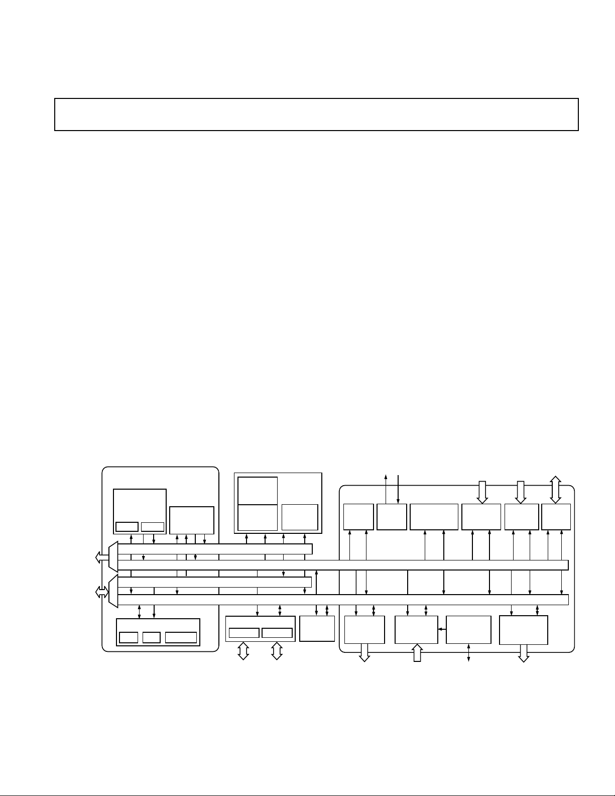
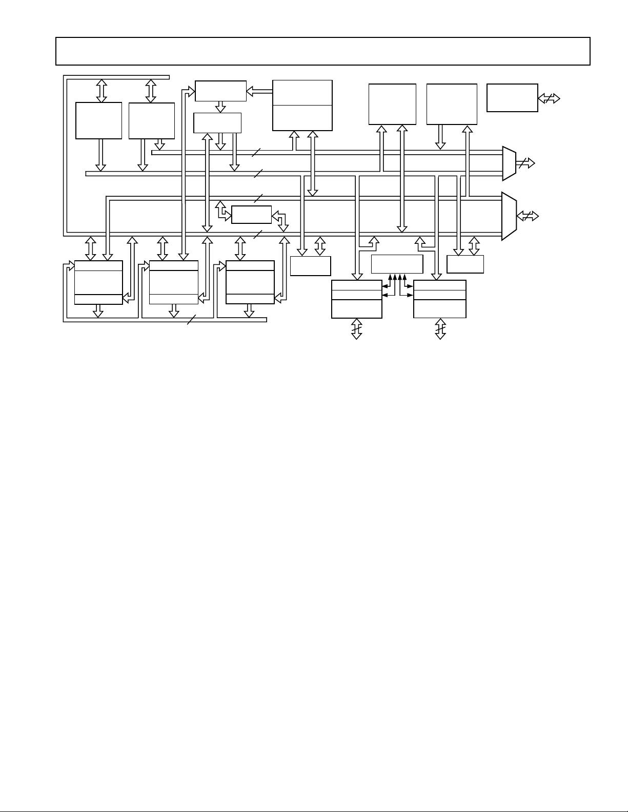
FUNCTIONAL BLOCK DIAGRAM
High Performance Motor Controller
ADMC401
Internal or External Voltage Reference
Out-of-Range Detection
Voltage Reference
Internal 2.0 V 2.0% Voltage Reference
Three-Phase 16-Bit PWM Generation Unit
Programmable Switching Frequency, Dead Time and
Minimum Pulsewidth
Edge Resolution of 38.5 ns
One or Two Updates per Switching Period
Hardware Polarity Control
Individual Enable/Disable of Each Output
High Frequency Chopping Mode
Dedicated Shutdown Pin (PWMTRIP)
Additional Shutdown Pins in I/O System
High Output Sink and Source Capability (10 mA)
Incremental Encoder Interface Unit
Quadrature Rates to 17.3 MHz
Programmable Filtering of Encoder Inputs
Alternative Frequency and Direction Mode
Two Registration Inputs to Latch Count Value
Optional Hardware Reset of Counter
Single North Marker Mode
Count Error Monitor Function
Dedicated 16-Bit Loop Timer (Periodic Interrupts)
Companion Encoder Event (1/T) Timer
(Continued on Page 14)
EXTERNAL
ADDRESS
BUS
EXTERNAL
DATA
BUS
26 MIPS DSP CORE
DATA
ADDRESS
GENERATORS
DAG 1
DAG 2
PROGRAM MEMORY ADDRESS
DATA MEMORY ADDRESS
PROGRAM MEMORY DATA
DATA MEMORY DATA
ARITHMETIC UNITS
ALU
MAC
PROGRAM
SEQUENCER
SHIFTER
PM
ROM
2K 24
PM
RAM
2K 24
SERIAL PORTS
SPORT 0
SPORT 1
MEMORY
DM
RAM
1K 16
REV. B
Information furnished by Analog Devices is believed to be accurate and
reliable. However, no responsibility is assumed by Analog Devices for its
use, nor for any infringements of patents or other rights of third parties
which may result from its use. No license is granted by implication or
otherwise under any patent or patent rights of Analog Devices.
MOTOR CONTROL
PERIPHERALS
WATCH-
TIMER
INTERVAL
TIMER
2 CHANNEL
AUXILIARY
One Technology Way, P.O. Box 9106, Norwood, MA 02062-9106, U.S.A.
Tel: 781/329-4700 World Wide Web Site: http://www.analog.com
Fax: 781/326-8703 © Analog Devices, Inc., 2000
DOG
PWM
POWER-
ON
RESET
INTERRUPT
CONTROLLER
8 CHANNEL
12-BIT ADC
ENCODER
INTERFACE
PRECISION
VOLTAGE
REFERENCE
EVENT
CAPTURE
UNIT
16-BIT
PWM
GENERATION
DIGITAL
I/O
UNIT

ADMC401–SPECIFICATIONS
(VDD = AVDD = 5 V 5%, GND = AGND = 0 V, T
RECOMMENDED OPERATING CONDITIONS
CLKIN = 13 MHz, unless otherwise noted)
B Grade
Parameter Min Max Unit
V
AV
T
DD
AMB
Digital Supply Voltage 4.75 5.25 V
Analog Supply Voltage 4.75 5.25 V
DD
Ambient Operating Temperature –40 +85 °C
ELECTRICAL CHARACTERISTICS
Parameter Test Conditions Min Max Unit
V
IH
V
IL
V
OH
V
OL
V
OH
V
OL
I
IH
I
IH
I
IH
I
IL
I
IL
I
IL
I
OZH
I
OZL
I
DD
I
DD
I
DD
C
I
C
O
NOTES
1
Bidirectional pins: D0–D23, RFS0, RFS1, TFS0, TFS1, SCLK0 and SCLK1, PIO0–PIO11.
2
Input only pins: PWMTRIP, PWMPOL, PWMSR, RESET, EIA, EIB, EIZ, EIS, ETU0, ETU1, DR1A, DR1B, DR0, CLKIN, CONVST, MMAP, BMODE, BR
and PWD.
3
Programmable I/O Pins (PIO0–PIO11).
4
Output pins: PWMSYNC, AUX0, AUX1, CLKOUT, DT0, DT1, BG, BGH, PMS, DMS, BMS, RD, WR, PWDACK and A0–A13.
5
Output pins: AH, AL, BH, BL, CH and CL.
6
Although specified for TTL outputs, all ADMC401 outputs are CMOS-compatible and will drive to VDD–0.3 V and GND+0.3 V assuming no dc loads.
7
Input only pins RESET, EIA, EIB, EIZ, EIS, ETU0, ETU1, DR1A, DR1B, DR0, CLKIN, CONVST, MMAP, BMODE, BR and PWD.
8
Input pins with internal pull-down PIO0–PIO11 and PWMTRIP.
9
Input pins with internal pull-up, PWMPOL and PWMSR.
10
Three-statable pins: A0–A13, D0–D23, PMS, DMS, BMS, RD, WR, DT0, DT1, RFS0, RFS1, TFS0, TFS1, SCLK0, SCLK1.
11
Idle refers execution of the IDLE instruction. Deasserted pins are driven to VDD or GND. Current reflects device operation with CLKOUT disabled.
12
Current reflects device operating with no output loads.
13
Guaranteed but not tested.
14
Output Pin Capacitance is the capacitive load for any three-state output pin.
Specifications subject to change without notice.
HI-Level Input Voltage
LO-Level Input Voltage
HI-Level Output Voltage
LO-Level Output Voltage
HI-Level Output Voltage
LO-Level Output Voltage
HI-Level Input Current
HI-Level Input Current
HI-Level Input Current
LO-Level Input Current
LO-Level Input Current
LO-Level Input Current
HI-Level Three-State Leakage Current
LO-Level Three-State Leakage Current
Digital Supply Current (Idle)
Digital Supply Current (Dynamic)
Analog Supply Current @ AVDD = max 60 mA
Input Pin Capacitance
Output Pin Capacitance
1, 2, 3
1, 2, 3
1, 3, 4, 5, 6
1, 3, 4, 5, 6
5
5
7
8
9
7
8
9
13
13, 14
@ VDD = max 2.0 V
@ VDD = min 0.8 V
@ VDD = min, IOH = –1.0 mA 2.4 V
@ V
= min, IOH = –0.1 mA VDD – 0.3 V
DD
@ VDD = min, IOL = 2.0 mA 0.4 V
@ VDD = min, IOH = –10.0 mA 2.4 V
@ VDD = min, IOL = 10.0 mA 1.2 V
@ VDD = max, VIN = VDD max 10 µA
@ VDD = max, VIN = V
@ VDD = max, VIN = V
max 100 µA
DD
max 10 µA
DD
@ VDD = max, VIN = 0 V 10 µA
@ VDD = max, VIN = 0 V 10 µA
10
10
11
12
@ VDD = max, VIN = 0 V 100 µA
@ VDD = max, VIN = V
max 10 µA
DD
@ VDD = max, VIN = 0 V 10 µA
@ VDD = max 40 mA
@ VDD = max 110 mA
VIN = 2.5 V, fIN = 1 MHz, 8 pF
= +25°C
T
AMB
VIN = 2.5 V, fIN = 1 MHz, 8 pF
T
= +25°C
AMB
= –40C to +85C,
AMB
–2–
REV. B

ADMC401
ANALOG-TO-DIGITAL CONVERTER
(VDD = AVDD = 5 V 5%, GND = AGND = 0 V, T
VIN0 to VIN7 = 4.0 V p-p, V
= 2.0 V, unless otherwise noted)
REF
= –40C to +85C, CLKIN = 13 MHz,
AMB
Parameter Test Conditions Min Typ Max Unit
AC SPECIFICATIONS
SNR Signal to Noise Ratio fIN = 1.0 kHz 68 70 dB
SNRD Signal to Noise and Distortion f
THD Total Harmonic Distortion f
CTLK Channel-Channel Crosstalk f
= 1.0 kHz 66 69 dB
IN
= 1.0 kHz –76 –70 dB
IN
= 1.0 kHz –89 –72 dB
IN
CMRR Common-Mode Rejection Ratio –90 –72 dB
PSRR Power Supply Rejection Ratio 0.025 0.1 % FSR
ACCURACY
INL Integral Nonlinearity ± 0.6 ± 1.5 LSB
DNL Differential Nonlinearity ± 0.5 ± 1.0 LSB
No Missing Codes 12 Bits Guaranteed
Zero Error 0.1 0.25 % FSR
Gain Error
1
0.4 1.0 % FSR
TEMPERATURE DRIFT
Zero Error 0.025 % FSR
Gain Error
1
0.025 % FSR
INPUT VOLTAGE
V
IN
C
IN
Voltage Span 4.0 V p-p
Input Capacitance
2
10 pF
CONVERSION TIME
t
CONV
NOTES
1
Excludes Internal Voltage Reference Error.
2
Analog Input Pins VIN0 to VIN7.
Typical values are neither tested nor guaranteed.
Specifications subject to change without notice.
Total Conversion Time All 8 Channels 1.88 µs
VOLTAGE REFERENCE
(VDD = AVDD = 5 V 5%, GND = AGND = 0 V, T
4.0 V p-p, V
= 2.0 V, unless otherwise noted)
REF
= –40C to +85C, CLKIN = 13 MHz, VIN0 to VIN7 =
AMB
Parameter Test Conditions Min Typ Max Unit
V
REF
Output Voltage Reference SENSE = REFCOM 1.96 2.0 2.04 V
Output Voltage Tolerance
1
SENSE = REFCOM 6 mV
Output Current 1.0 mA
Load Regulation 1.0 mA Load Current 0.3 1.5 mV
Power Supply Rejection Ratio 0.1 1.5 mV
Reference Input Resistance 8 kΩ
NOTES
1
Relative tolerance due to temperature change, T
Specifications subject to change without notice.
POWER-ON RESET
(GND = AGND = 0 V, T
MIN
to T
.
MAX
= –40C to +85C, CLKIN = 13 MHz, unless otherwise noted)
AMB
Parameter Test Conditions Min Typ Max Unit
V
RST
V
HYST
Specifications subject to change without notice.
Reset Threshold Voltage 3.25 4.0 V
Hysteresis Voltage 75 mV
REV. B
–3–

ADMC401
WARNING!
ESD SENSITIVE DEVICE
ABSOLUTE MAXIMUM RATINGS*
Supply Voltage . . . . . . . . . . . . . . . . . . . . . . . . . . –0.3 V to +7 V
Input Voltage . . . . . . . . . . . . . . . . . . . . . –0.3 V to V
Output Voltage Swing . . . . . . . . . . . . . . –0.3 V to V
Operating Temperature Range (Ambient) . . . . –40°C to +85°C
Storage Temperature Range . . . . . . . . . . . . . –65°C to +150°C
Lead Temperature (5 sec) . . . . . . . . . . . . . . . . . . . . . . +280°C
*Stresses above those listed under absolute maximum ratings may cause permanent
damage to the device. These are stresses only; functional operation of the device
at these or any other conditions above those indicated in the operational section of
this specification is not implied. Exposure to absolute maximum rating conditions
for extended periods may affect device reliability.
Temperature Instruction Package Package
Model Range Rate Description Option
ADMC401BST –40°C to +85°C 26 MHz 144-Lead Plastic Thin Quad Flatpack (LQFP) ST-144
ADMC401-ADVEVALKIT Development Tool Kit
ADMC401-PB Evaluation/Processor Board
CAUTION
ESD (electrostatic discharge) sensitive device. Electrostatic charges as high as 4000 V readily
accumulate on the human body and test equipment and can discharge without detection.
Although the ADMC401 features proprietary ESD protection circuitry, permanent damage may
occur on devices subjected to high-energy electrostatic discharges. Therefore, proper ESD
precautions are recommended to avoid performance degradation or loss of functionality.
+ 0.3 V
DD
+ 0.3 V
DD
ORDERING GUIDE
Timing Parameters
GENERAL NOTES
Use the exact timing information given. Do not attempt to
derive parameters from the addition or subtraction of others.
While addition or subtraction would yield meaningful results for
an individual device, the values given in this data sheet reflect
statistical variations and worst cases. Consequently, you cannot
meaningfully add up parameters to derive longer times.
TIMING NOTES
Switching characteristics specify how the processor changes its
signals. You have no control over this timing; it is dependent on
the internal design. Timing requirements apply to signals that
are controlled outside the processor, such as the data input for a
read operation.
Timing requirements guarantee that the processor operates
correctly with another device. Switching characteristics tell you
what the device will do under a given circumstance. Also, use
the switching characteristics to ensure any timing requirement
of a device connected to the processor (such as memory) is
satisfied.
MEMORY REQUIREMENTS
This chart links common memory device specification names
and ADMC401 timing parameters for your convenience.
Common
Parameter Memory Device
Name Function Specification Name
t
ASW
t
AW
t
WRA
t
DW
t
DH
t
RDD
t
AA
A0–A13, DMS, PMS Address Setup to
Setup before WR Low Write Start
A0–A13, DMS, PMS Address Setup to
before WR Deasserted Write End
A0–A13, DMS, PMS Address Hold Time
Hold after WR Deasserted
Data Setup before WR High Data Setup Time
Data Hold after WR High Data Hold Time
RD Low to Data Valid OE to Data Valid
A0–A13, DMS, PMS, Address Access Time
BMS to Data Valid
–4–
REV. B
ADMC401
Parameter Min Max Unit
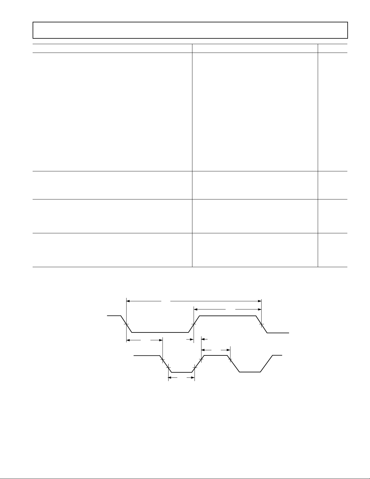
Clock Signals
t
is defined as 0.5t
CK
with a frequency equal to half the instruction rate; a 13 MHz
clock (which is equivalent to 76.9 ns) yields a 38.5 ns processor
cycle (equivalent to 26 MHz). t
0.5t
period should be substituted for all relevant timing
CKI
parameters to obtain specification value.
Example: t
= 0.5tCK – 10 ns = 0.5 (38.5 ns) – 10 ns = 9.25 ns.
CKH
Timing Requirements:
t
CKI
t
CKIL
t
CKIH
Switching Characteristics:
t
CKL
t
CKH
t
CKOH
Control Signals
Timing Requirement:
t
RSP
PWM Shutdown Signals
Timing Requirements:
t
PWMTPW
t
PIOPWM
ADC Signals
Timing Requirements:
t
CSI
t
CSE
NOTE
1
Applies after power-up sequence is complete. Internal phase lock loop requires no more than 2000 CLKIN cycles assuming stable CLKIN (not including crystal
oscillator start-up time).
The ADMC401 uses an input clock
CKI.
values within the range of
CK
CLKIN Period 76.9 150 ns
CLKIN Width Low 20 ns
CLKIN Width High 20 ns
CLKOUT Width Low 0.5t
CLKOUT Width High 0.5t
– 10 ns
CK
– 10 ns
CK
CLKIN High to CLKOUT High 0 20 ns
CK
CK
CK
CK
CK
1
ns
ns
ns
ns
ns
RESET Width Low 5t
PWMTRIP Width Low t
PIO Width Low 2t
Internal Convert Start Width High 2t
External Convert Start Width High 2t
REV. B
CLKIN
CLKOUT
t
t
CKI
CKIL
t
CKL
Figure 1. Clock Signals
–5–
t
CKOH
t
CKIH
t
CKH
ADMC401
Parameter Min Max Unit
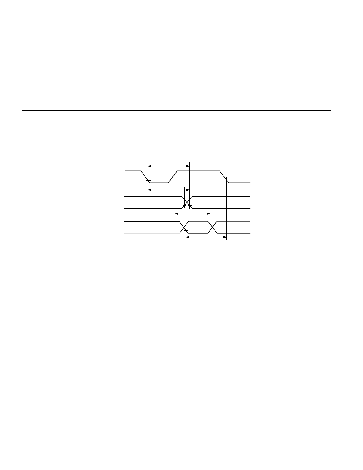
Interrupts and Flags
Timing Requirements:
t
t
IFS
IFH
IRQx or FI Setup before CLKOUT Low
IRQx or FI Hold after CLKOUT High
Switching Characteristics:
t
FOH
t
FOD
NOTES
1
If IRQx and FI inputs meet t
the following cycle. (Refer to “Interrupt Controller Operation” in the Program Control chapter of the ADSP-2100 Family User’s Manual, Third Edition for further
information on interrupt servicing.)
2
Edge-sensitive interrupts require pulsewidths greater than 10 ns; level-sensitive interrupts must be held low until serviced.
3
IRQx = IRQ0 and IRQ1.
4
Flag Output = FL1 and FO.
Flag Output Hold after CLKOUT Low
Flag Output Delay from CLKOUT Low
and t
IFS
setup/hold requirements, they will be recognized during the current clock cycle; otherwise the signals will be recognized on
IFH
CLKOUT
FLAG
OUTPUTS
1, 2, 3
1, 2, 3
4
4
0.25tCK + 15 ns
0.25t
CK
ns
0.5tCK – 7 ns
0.5tCK + 5 ns
t
FOD
t
FOH
t
IFH
IRQx
FI
t
IFS
Figure 2. Interrupts and Flags
–6–
REV. B
ADMC401
Parameter Min Max Unit
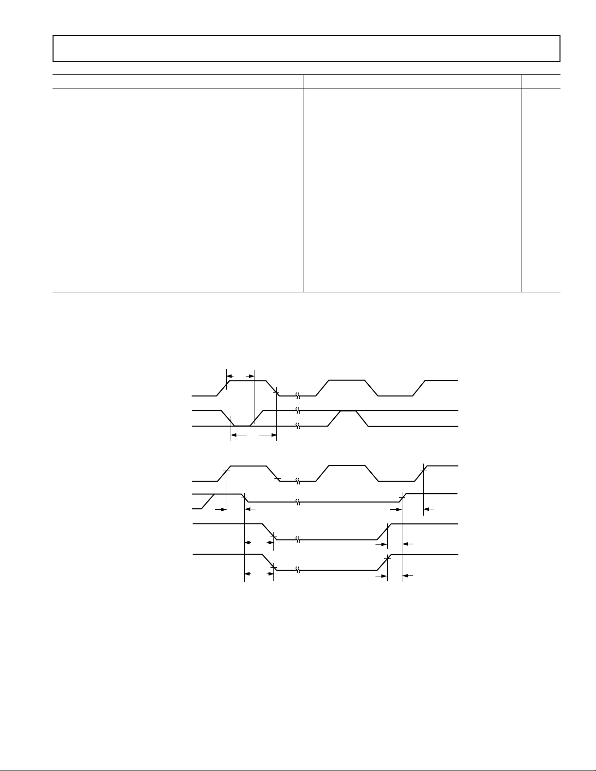
Bus Request/Grant
Timing Requirements:
t
BH
t
BS
BR Hold after CLKOUT High
BR Setup before CLKOUT Low
Switching Characteristics:
t
SD
CLKOUT High to DMS, PMS, BMS, 0.25tCK + 10 ns
RD, WR Disable
t
SDB
DMS, PMS, BMS, RD, WR
Disable to BG Low 0 ns
t
SE
BG High to DMS, PMS, BMS,
RD, WR Enable 0 ns
t
SEC
DMS, PMS, BMS, RD, WR
Enable to CLKOUT High 0.25t
t
SDBH
t
SEH
NOTES
1
BR is an asynchronous signal. If BR meets the setup/hold requirements, it will be recognized during the current clock cycle; otherwise the signal will be recognized
on the following cycle. Refer to the ADSP-2100 Family User’s Manual, Third Edition for BR/BG cycle relationships.
2
BGH is asserted when the bus is granted and the processor requires control of the bus to continue.
DMS, PMS, BMS, RD, WR
Disable to BGH Low
BGH High to DMS, PMS, BMS,
RD, WR Enable
2
2
1
1
0.25tCK +2 ns
0.25tCK + 17 ns
– 7 ns
CK
0ns
0ns
CLKOUT
BR
CLKOUT
PMS, DMS
BMS, RD
WR
BG
BGH
t
BH
t
BS
t
SD
t
SDB
t
SDBH
Figure 3. Bus Request–Bus Grant
t
SEC
t
SE
t
SEH
REV. B
–7–
ADMC401
Parameter Min Max Unit
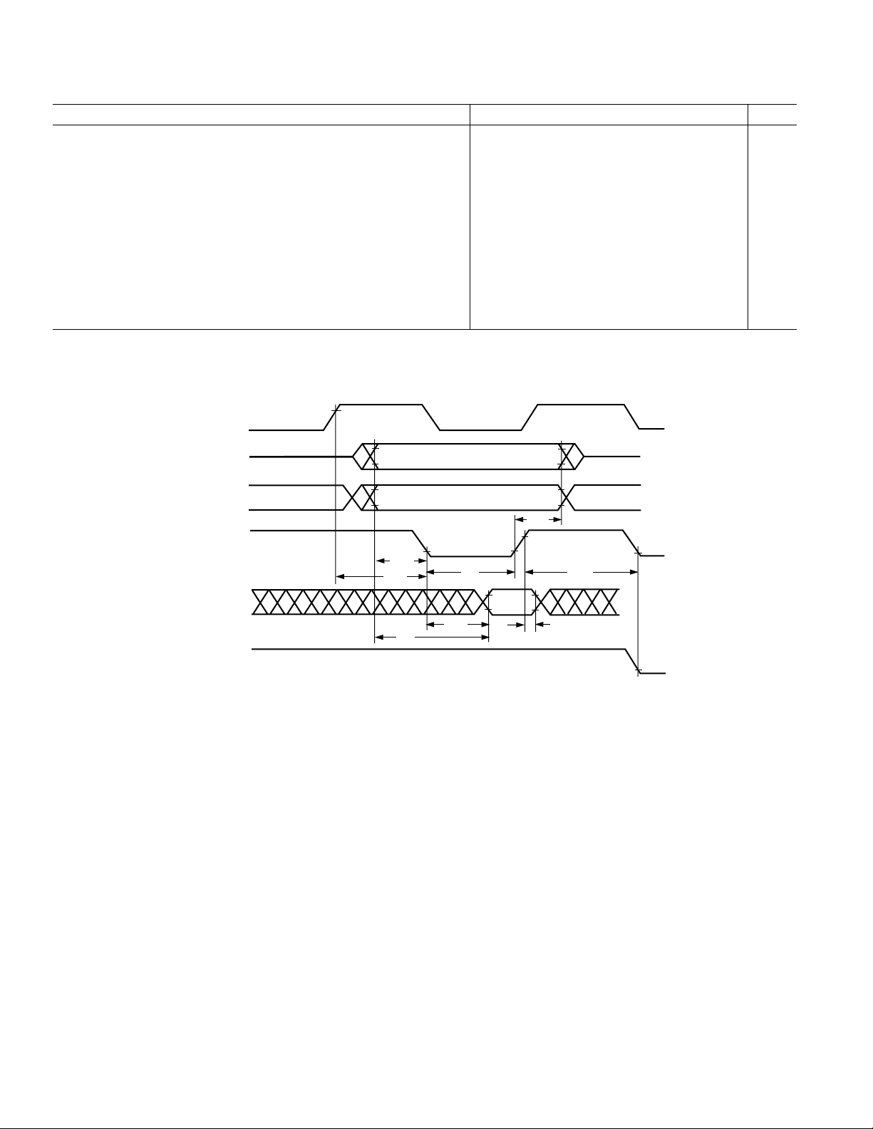
Memory Read
Timing Requirements:
t
RDD
t
AA
t
RDH
Switching Characteristics:
t
RP
t
CRD
t
ASR
t
RDA
t
RWR
w = wait states × tCK.
RD Low to Data Valid 0.5tCK – 11 + w ns
A0–A13, PMS, DMS, BMS to Data Valid 0.75tCK – 12 + w ns
Data Hold from RD High 0 ns
RD Pulsewidth 0.5tCK – 5 + w ns
CLKOUT High to RD Low 0.25tCK – 5 0.25tCK + 7 ns
A0–A13, PMS, DMS, BMS Setup before RD Low 0.25tCK – 6 ns
A0–A13, PMS, DMS, BMS Hold after RD Deasserted 0.25tCK – 3 ns
RD High to RD or WR Low 0.5t
CLKOUT
A0–A13
– 5 ns
CK
DMS, PMS
BMS
RD
WR
t
RDA
t
ASR
t
CRD
D
t
AA
t
RP
t
RDD
t
RWR
t
RDH
Figure 4. Memory Read
–8–
REV. B
ADMC401
Parameter Min Max Unit
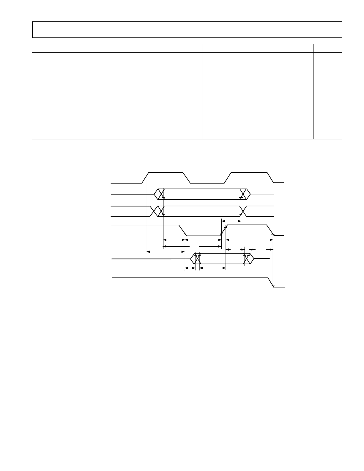
Memory Write
Switching Characteristics:
t
DW
t
DH
t
WP
t
WDE
t
ASW
t
DDR
t
CWR
t
AW
t
WRA
t
WWR
w = wait states × tCK.
Data Setup before WR High 0.5t
Data Hold after WR High 0.25t
– 7 + w ns
CK
– 2 ns
CK
WR Pulsewidth 0.5tCK – 5 + w ns
WR Low to Data Enabled 0 ns
A0–A13, DMS, PMS Setup before WR Low 0.25t
– 6 ns
CK
Data Disable before WR or RD Low 0.25tCK – 6 ns
CLKOUT High to WR Low 0.25t
A0–A13, DMS, PMS, Setup before WR Deasserted 0.75t
A0–A13, DMS, PMS Hold after WR Deasserted 0.25t
– 5 0.25tCK + 7 ns
CK
– 9 + w ns
CK
– 3 ns
CK
WR High to RD or WR Low 0.5tCK – 5 ns
CLKOUT
A0–A13
DMS, PMS
WR
RD
t
WRA
t
ASW
t
CWR
D
t
WP
t
AW
t
t
WDE
DW
t
WWR
t
DH
t
DDR
Figure 5. Memory Write
REV. B
–9–
ADMC401
(
)
Parameter Min Max Unit
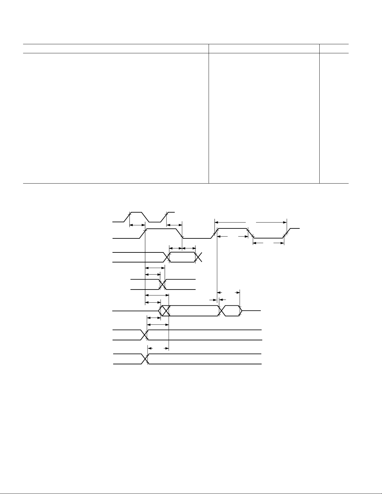
Serial Ports
Timing Requirements:
t
SCK
t
SCS
t
SCH
t
SCP
Switching Characteristics:
t
CC
t
SCDE
t
SCDV
t
RH
t
RD
t
SCDH
t
TDE
t
TDV
t
SCDD
t
RDV
SCLK Period 50 ns
DR/TFS/RFS Setup before SCLK Low 5 ns
DR/TFS/RFS Hold after SCLK Low 10 ns
SCLK
CLKOUT High to SCLK
Width 20 ns
IN
OUT
0.25t
CK
0.25t
+ 15 ns
CK
SCLK High to DT Enable 0 ns
SCLK High to DT Valid 20 ns
TFS/RFS
TFS/RFS
Hold after SCLK High 0 ns
OUT
Delay from SCLK High 20 ns
OUT
DT Hold after SCLK High 0 ns
TFS(Alt) to DT Enable 0 ns
TFS(Alt) to DT Valid 20 ns
SCLK High to DT Disable 20 ns
RFS (Multichannel, Frame Delay Zero) to DT Valid 20 ns
CLKOUT
SCLK
DR
RFS
TFS
RFS
OUT
TFS
OUT
TFS
alternate
frame mode
multichannel mode,
RFS
frame delay 0
MFD = 0
DT
t
CC
IN
IN
t
t
t
RD
t
RH
SCDV
SCDE
t
TDE
t
TDV
t
CC
t
SCS tSCS
t
t
SCDH
t
RDV
SCDD
t
SCK
t
SCP
t
SCP
Figure 6. Serial Ports
–10–
REV. B
ADMC401
POWER DISSIPATION
To determine total power dissipation in a specific application,
the following equation should be applied for each output:
2
DD
× f
C × V
C = load capacitance, f = output switching frequency.
Example:
In an application where external data memory is used and no
other outputs are active, power dissipation is calculated as
follows:
Assumptions:
• External data memory is accessed every cycle with 50% of the
address pins switching.
• External data memory writes occur every other cycle with
50% of the data pins switching.
• Each address and data pin has a 10 pF total load at the pin.
• The application operates at V
Total Power Dissipation = P
= VDD × (IDD Digital + IDD Analog)
P
INT
(C × V
2
× f) is calculated for each output:
DD
# of
Pins C V
Address, DMS 8 × 10 pF × 52 V × 26 MHz = 52.00 mW
Data Output, WR 9 × 10 pF × 52 V × 13 MHz = 29.25 mW
RD 1 × 10 pF × 52 V × 13 MHz = 3.25 mW
CLKOUT 1 × 10 pF × 52 V × 26 MHz = 6.50 mW
Total power dissipation for this example is P
= 5.0 V and t
DD
+ (C × V
INT
2
f
DD
= 38.5 ns.
CK
2
× f)
DD
+ 91 mW.
INT
91.00 mW
INPUT
OUTPUT
0.0V
0.3V
1.5V
2.0V
1.5V
3.0V
Figure 7. Voltage Reference Levels for AC Measurements (Except Output Enable/Disable)
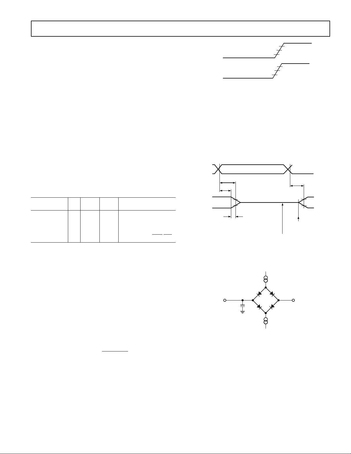
Output Enable Time
Output pins are considered to be enabled when that have made
a transition from a high-impedance state to when they start
driving. The output enable time (t
) is the interval from when
ENA
a reference signal reaches a high or low voltage level to when
the output has reached a specified high or low trip point, as
shown in the Output Enable/Disable diagram. If multiple pins
(such as the data bus) are enabled, the measurement value is
that of the first pin to start driving.
REFERENCE
SIGNAL
t
(MEASURED)
OUTPUT
(MEASURED)
V
OH
V
OL
MEASURED
t
DIS
V
(MEASURED) – 0.5V
OH
(MEASURED) +0.5V
V
OL
t
DECAY
OUTPUT STOPS
DRIVING
HIGH-IMPEDANCE STATE. TEST CONDITIONS CAUSE
THIS VOLTAGE LEVEL TO BE APPROXIMATELY 1.5V.
t
ENA
V
(MEASURED)
2.0V
1.0V
OUTPUT STARTS
DRIVING
V
(MEASURED)
OH
OL
Figure 8. Output Enable/Disable
TEST CONDITIONS
Output Disable Time
Output pins are considered to be disabled when they have
stopped driving and started a transition from the measured
output high or low voltage to a high impedance state. The output disable time (t
) is the difference of t
DIS
MEASURED
and t
DECAY
,
as shown in the Output Enable/Disable diagram. The time is the
interval from when a reference signal reaches a high or low
voltage level to when the output voltages have changed by 0.5 V
from the measured output high or low voltage. The decay time,
, is dependent on the capacitative load, CL, and the cur-
t
DECAY
rent load, i
, on the output pin. It can be approximated by the
L
following equation:
CV
× 05.
t
DECAY
L
=
I
L
from which
tt t
=−
DIS MEASURED DECAY
is calculated. If multiple pins (such as the data bus) are disabled, the measurement value is that of the last pin to stop
driving.
I
OL
OUTPUT
PIN
TO
50pF
I
OH
+1.5V
Figure 9. Equivalent Device Loading for AC Measurements (Including All Fixtures)
REV. B
–11–

ADMC401
PIN FUNCTION DESCRIPTION
Pin Pin Pin Pin Pin Pin Pin Pin
No. Name No. Name No. Name No. Name
1 A9 37 RFS1/IRQ0/SROM 73 GND 109 CONVST
2 A8 38 TFS1/IRQ1 74 D10 110 GND
3 A7 39 SCLK1 75 D9 111 VDD
4 A6 40 DR0 76 D8 112 GND
5 VDD 41 DT0 77 D7 113 AVDD
6 A5 42 RFS0 78 D6 114 AVSS
7 A4 43 TFS0 79 D5 115 VIN7
8 A3 44 SCLK0 80 D4 116 V
9 GND 45 VDD 81 D3 117 VIN6
10 A2 46 GND 82 GND 118 REFCOM
11 A1 47 PWMTRIP 83 D2 119 VIN5
12 A0 48 PWMSYNC 84 D1 120 CAPT
13 PWD 49 CL 85 D0 121 VIN4
14 PWDACK 50 CH 86 P11 122 BSHAN
15 BR 51 VDD 87 P10 123 ASHAN
16 NC 52 GND 88 P9 124 VIN0
17 NC 53 BL 89 P8 125 CAPB
18 BMODE 54 BH 90 VDD 126 VIN1
19 MMAP 55 AL 91 GND 127 CML
20 VDD 56 AH 92 P7 128 VIN2
21 GND 57 BGH 93 P6 129 GAIN
22 PWMSR 58 D23 94 P5 130 VIN3
23 POR 59 D22 95 P4 131 SENSE
24 RESET 60 D21 96 P3 132 AVSS
25 GND 61 D20 97 P2 133 AVDD
26 GND 62 D19 98 GND 134 BMS
27 GND 63 GND 99 P1 135 PMS
28 PWMPOL 64 D18 100 P0 136 DMS
29 CLKIN 65 D17 101 AUX1 137 RD
30 XTAL 66 D16 102 AUX0 138 GND
31 CLKOUT 67 D15 103 ETU1 139 BG
32 VDD 68 D14 104 ETU0 140 WR
33 GND 69 D13 105 EIS 141 A13
34 DR1A/FI 70 D12 106 EIZ 142 A12
35 DRIB/FI 71 VDD 107 EIB 143 A11
36 DT1/FO 72 D11 108 EIA 144 A10
NC: These pins must be left unconnected
REF
–12–
REV. B

PIN CONFIGURATION
A9A8A7
A6
VDD
A5A4A3
GND
A2A1A0
PWD
PWDACK
BRNCNC
BMODE
MMAP
VDD
GND
PWMSR
POR
RESET
GND
GND
GND
PWMPOL
CLKIN
XTAL
CLKOUT
VDD
GND
DR1A/F1
DR1B/FI
DT1/FO
P1
GNDP2P3P4P5P6P7
GND
VDDP8P9
P10
P11D0D1D2GNDD3D4D5D6D7D8D9D10
GND
EIA
EIB
EIZ
EIS
ETU0
ETU1
AUX0
AUX1
P0
D11
VDD
D12
D13
D14
D15
D16
D17
D18
GND
D19
D20
D21
D22
D23
BGH
AH
AL
BH
BL
GND
VDD
CH
CL
PWMSYNC
PWMTRIP
GND
VDD
SCLK0
TFS0
RFS0
DT0
DR0
SCLK1
TFS1/IRQ1
RFS1/IRQ0/SROM
CONVST
GND
VDD
GND
AVDD
AVSS
VIN7
V
REF
VIN6
REFCOM
VIN5
CAPT
VIN4
BSHAN
ASHAN
VIN0
CAPB
VIN1
CML
VIN2
GAIN
VIN3
SENSE
AVSS
AVDD
BMS
PMS
DMS
RD
GND
BG
WR
A13
A12
A11
A10
NC = NO CONNECT
PIN 1
IDENTIFIER
TOP VIEW
(Not to Scale)
ADMC401
1920212223242526272829303132333435
36
101112131415161718
123456789
9089888786858483828180797877767574
73
999897969594939291
108
107
106
105
104
103
102
101
100
72
71
70
69
68
67
66
65
64
63
62
61
60
59
58
57
56
55
54
53
52
51
50
49
48
47
46
45
44
43
42
41
40
39
38
37
109
110
111
112
113
114
115
116
117
118
119
120
121
122
123
124
125
126
127
128
129
130
131
132
133
134
135
136
137
138
139
140
141
142
143
144
ADMC401
REV. B
–13–

ADMC401
(Continued from Page 1)
Programmable Digital I/O (PIO) Port
12-Pin Configurable Digital I/O Port
Flexible Interrupt Generation
Four Dedicated PIO Interrupt Vectors
Each I/O Line Configurable as PWM Shutdown
Two 8-Bit Auxiliary PWM Outputs
Programmable Switching Frequency
Independent or Offset Modes
Two-Channel Event Timer (Capture) Unit
Configurable Event Definition
Single-Shot or Free-Running Modes
Peripheral Interrupt Controller
Manages Peripheral Interrupts
16-Bit Watchdog Timer
Internal Power-On Reset System
Programmable 16-Bit Interval Timer with Prescaler
Two Double Buffered Synchronous Serial Ports
Boot Load Protocols via SPORT1:
Synchronous E
UART Boot Loader with Autobaud
Synchronous Master or Slave Boot Loader
Debugger Interface via SPORT1:
UART Interface with Autobaud
Synchronous Master or Slave Interface
Full Debugger for Program Development
Industrial Temperature Range –40C to +85C
Operating Voltage 5.0 V 5%
Package: 144-Lead LQFP
GENERAL DESCRIPTION
2
PROM/SROM Booting
The ADMC401 is a single-chip DSP-based controller, suitable
for high performance control of ac induction motors (ACIM),
permanent magnet synchronous motors (PMSM), brushless dc
motors (BDCM) and switched reluctance (SR) motors in industrial applications. The ADMC401 integrates a 26 MIPS, fixedpoint DSP core with a complete set of motor control peripherals
that permits fast motor control in a highly integrated environment.
The DSP core of the ADMC401 is the ADSP-2171 which is
completely code compatible with the ADSP-21xx DSP family
(as well as other members of the integrated motor controllers of
the ADMC3xx family) and combines three computational units,
data address generators and a program sequencer. The computational units comprise an ALU, a multiplier/accumulator (MAC)
and a barrel shifter. The DSP core also adds instructions for bit
manipulation, squaring (x
2
), biased rounding and global interrupt masking. In addition, two flexible double-buffered, bidirectional synchronous serial ports are included in the ADMC401.
The ADMC401 provides 2K × 24-bit internal program memory
RAM, 2K × 24-bit internal program memory ROM and 1K ×
16-bit internal data memory RAM. The program and data
memory RAM can be boot loaded through the serial port from
either a serial E
2
PROM, through a UART connection (either
from external host microprocessor or from the Motion Control
Debugger) or via a synchronous serial interface from a host
microprocessor. Alternatively, the internal program and data
memory RAM may be booted from an external device across the
address and data buses. The program memory ROM includes a
monitor that adds software debugging features through the serial
port.
Additionally, the ADMC401 device adds significant external
memory and peripheral expansion capabilities by making available the full address and data bus of the DSP core. This feature
permits expansion of both external program and data memory
and means that the DSP core can address up to 14K × 24 bits of
external program memory and up to 13K × 16 bits of external
data memory.
The ADMC401 contains a number of special purpose, motor
control peripherals. The first is a high performance, 8-channel,
12-bit ADC system with dual channel simultaneous sampling
ability across 4 pair of inputs. An internal precision voltage reference is also available as part of the ADC system. In addition, a
three-phase, 16-bit, center-based PWM generation unit can be
used to produce high-accuracy PWM signals with minimal processor overhead. The ADMC401 also contains a flexible incremental encoder interface unit for position sensor feedback;
two adjustable-frequency auxiliary PWM outputs, 12 lines of
digital I/O; a 2-channel event capture system; a 16-bit watchdog
timer; two 16-bit interval timers (one of which can be linked to
the encoder interface unit) and an interrupt controller that manages all peripheral interrupts. Finally, the ADMC401 contains
an integrated power-on-reset (POR) circuit that can be used to
generate the required reset signal for the device on power-on.
–14–
REV. B
ADMC401
DATA
ADDRESS
GENERATOR
#1
INPUT REGS
ALU
OUTPUT REGS
DATA
ADDRESS
GENERATOR
#2
INPUT REGS
OUTPUT REGS
MAC
INSTRUCTION
PROGRAM
SEQUENCER
16
R BUS
REGISTER
OUTPUT REGS
PM ROM
2K 24
PM RAM
2K 24
CONTROL
LOGIC
PMA BUS
DMA BUS
PMD BUS
DMD BUS
TRANSMIT REG
RECEIVE REG
SERIAL
PORT 0
5
14
14
24
BUS
EXCHANGE
16
INPUT REGS
SHIFTER
Figure 10. DSP Core Block Diagram
DM RAM
1K 16
COMPANDING
CIRCUITRY
BOOT
ADDRESS
GENERATOR
TRANSMIT REG
RECEIVE REG
SERIAL
PORT 1
6
TIMER
POWER DOWN
CONTROL
LOGIC
14
24
2
EXTERNAL
ADDRESS BUS
EXTERNAL
DATA BUS
ARCHITECTURE OVERVIEW
Figure 10 is a functional block diagram of the DSP core of the
ADMC401. The DSP core is based on the fixed-point ADSP2171 core that is a member of the fixed-point ADSP-21xx
family of general purpose DSPs from Analog Devices Inc.
The ADSP-2171 flexible architecture and comprehensive instruction set allow the processor to perform multiple operations
in parallel.
In one processor cycle (38.5 ns with a 13 MHz crystal) the DSP
core can:
• Generate the next program address.
• Fetch the next instruction.
• Perform one or two data moves.
• Update one or two data address pointers.
• Perform a computational operation.
This all takes place while the ADMC401 continues to:
• Receive and transmit through the serial ports.
• Decrement the interval timers.
• Generate PWM signals.
• Convert the ADC input signals.
• Operate the encoder interface unit.
• Operate all other peripherals including the auxiliary PWM and
event timer subsystem.
The processor contains three independent computational units:
the arithmetic and logic unit (ALU), the multiplier/accumulator
(MAC) and the shifter. The computational units process 16-bit
data directly and have provisions to support multiprecision
computations. The ALU performs a standard set of arithmetic
and logic operations; division primitives are also supported. The
MAC performs single-cycle multiply, multiply/add, multiply/
subtract operations with 40 bits of accumulation. The shifter
performs logical and arithmetic shifts, normalization, denormalization and derive exponent operations. The shifter can be used
to implement numeric format control efficiently, including
floating-point representations. The internal result (R) bus directly connects the computational units so that the output of
any unit may be the input of any unit on the next cycle.
A powerful program sequencer and two dedicated data address
generators ensure efficient delivery of operands to these computational units. The sequencer supports conditional jumps, subroutine calls and returns in a single cycle. With internal loop
counters and loop stacks, the ADMC401 executes looping code
with zero overhead; no explicit jump instructions are required to
maintain the loop.
REV. B
–15–

ADMC401
Two data address generators (DAGs) provide addresses for
simultaneous dual operand fetches from data memory and program memory. Each DAG maintains and updates four address
pointers (I registers). Whenever the pointer is used to access
data (indirect addressing), it is post-modified by the value in
one of four modify (M) registers. A length value may be associated with each pointer (L registers) to implement automatic
modulo addressing for circular buffers. The circular buffering
feature is also used by the serial ports for automatic data transfers to and from on-chip memory. DAG1 generates only data
memory addresses but provides an optional bit-reversal capability. DAG2 may generate either program or data memory addresses, but has no bit-reversal capability.
Efficient data transfer is achieved with the use of five internal
buses:
• Program Memory Address (PMA) Bus.
• Program Memory Data (PMD) Bus.
• Data Memory Address (DMA) Bus.
• Data Memory Data (DMD) Bus.
• Result (R) Bus.
Program memory can store both instructions and data, permitting the ADMC401 to fetch two operands in a single cycle, one
from internal program memory and one from internal data
memory. The ADMC401 can fetch an operand from on-chip
program memory and the next instruction in the same cycle.
The ADMC401 writes data from its 16-bit registers to the 24bit program memory using the PX register to provide the lower
eight bits. When it reads data (not instructions) from 24-bit
program memory to a 16-bit data register, the lower eight bits
are placed in the PX register.
The ADMC401 can respond to a number of distinct DSP core
and peripheral interrupts. The DSP core interrupts include
serial port receive and transmit interrupts, timer interrupts,
software interrupts and external interrupts. In addition, there is
a master RESET signal. The motor control peripherals also
produce interrupts to the DSP core.
The two serial ports (SPORTs) provide a complete synchronous
serial interface with optional companding in hardware and a
wide variety of framed and unframed data transmit and receive
modes of operation. Each SPORT can generate an internal
programmable serial clock or accept an external serial clock.
Boot loading of both the program and data memory RAM of the
ADMC401 can be through the serial port SPORT1. Alternatively the ADMC401 can be boot loaded from an external bytewide memory connected to the external address and data buses.
After reset, seven wait states are automatically generated. This
permits, for example, a 38.5 ns ADMC401 to use an external
250 ns EPROM as boot memory. The internal boot address
generator provides the addresses for booting from an external
byte-wide memory.
A programmable interval counter is also included in the DSP
core and can be used to generate periodic interrupts. A 16-bit
count register (TCOUNT) is decremented every n processor
cycles, where n-1 is a scaling value stored in the 8-bit TSCALE
register. When the value of the counter reaches zero, an interrupt is generated and the count register is reloaded from a 16bit period register (TPERIOD).
The ADMC401 instruction set provides flexible data moves and
multifunction (one or two data moves with a computation)
instructions. Each instruction is executed in a single 38.5 ns
processor cycle (for a 13 MHz crystal). The ADMC401 assembly language uses an algebraic syntax for ease of coding and
readability. A comprehensive set of development tools supports
program development.
Serial Ports
The ADMC401 incorporates two complete synchronous serial
ports (SPORT0 and SPORT1) for serial communications and
multiprocessor communication. The following is a brief list of
the capabilities of the ADMC401 SPORTs. Refer to the ADSP-
2100 Family User’s Manual, Third Edition for further details.
• SPORTs are bidirectional and have a separate, double buffered transmit and receive section.
• SPORTs can use an external serial clock or generate their
own serial clock internally.
• SPORTs have independent framing for the receive and trans-
mit sections. Sections run in a frameless mode or with frame
synchronization signals internally or externally generated.
Frame synchronization signals are active high or inverted,
with either of two pulsewidths and timings.
SPORTs support serial data word lengths from 3 bits to 16
bits and provide optional A-law and µ-law companding.
• SPORT receive and transmit sections can generate unique
interrupts on completing a data word transfer.
• SPORTs can receive and transmit an entire circular buffer of
data with only one overhead cycle per data word. An interrupt is generated after a data buffer transfer.
• SPORT0 has a multichannel interface to selectively receive
and transmit a 24-word or 32-word, time-division multiplexed, serial bitstream.
• SPORT1 can be configured to have two external interrupts
(IRQ0 and IRQ1), and the Flag In and Flag Out signals. The
internally generated serial clock may still be used in this
configuration.
The following are additional capabilities of the ADMC401
SPORTs that are not part of the ADSP-21xx products:
• SPORT1 is the input for single pin program and data
memory boot loading. The RFS1 pin can be configured
internally to the ADMC401 as an SROM/E
signal.
• SPORT1 has two data receive pins (DR1A and DR1B). The
DR1A pin is intended only for synchronous data receive
from the external E
the data receive pin for a general purpose SPORT after booting or as the data receive pin for other boot load modes or as
the UART/debugger interface. The DR1A and DR1B pins
are internally multiplexed onto the one data receive pin of
the SPORT. The particular data receive pin selected is determined by Bit 4 of the MODECTRL register.
2
PROM. The DR1B pin can be used as
2
PROM reset
–16–
REV. B

ADMC401
PIN FUNCTION DESCRIPTION
The ADMC401 is available in an 144-lead TQFP package. Table
I contains the pin descriptions.
Table I. Pin List
Pin #
Group of Input/
Name Pins Output Function
A13–A0 14 O Address Lines
D23–D0 24 I/O Data Lines
PMS, DMS, BMS 3 O External Memory Select Lines
RD, WR 2 O External Memory Read/Write Enable
MMAP 1 I Memory Map Select
POR 1 O Internal Power On Reset Output
RESET 1 I Processor Reset Input
CLKOUT 1 O Processor Clock Output
CLKIN, XTAL 2 I, O External Clock or Quartz Crystal
Input
BR 1 I Bus Request
BG, BGH 2 O Bus Grant and Bus Hang Control
BMODE 1 I Boot Mode Select
PWD, PWDACK 2 I, O Power-Down and Power-Down
Acknowledge
SPORT0 5 I/O Serial Port 0 Pins (TFS0, RFS0,
DT0, DR0, SCLK0)
SPORT1 6 I/O Serial Port 1 (TFS1/IRQ1, RFS1/
IRQ0/SROM, DT1/FO, DR1A/FI,
DR1B/FI, SCLK1)
VIN0–VIN7 8 I Analog Inputs
ASHAN, BSHAN 2 I Inverting Inputs to Sample and
Hold Amplifiers
GAIN 1 I Analog Input for Gain Calibration
V
REF
REFCOM 1 GND Reference Common
CML 1 O Common-
CAPT, CAPB 2 O Noise Reduction Pins
SENSE 1 I Voltage Reference Select
CONVST 1 I External Convert Start
AH-CL 6 O PWM Outputs
PWMTRIP 1 I PWM Shutdown Signal
PWMPOL 1 I PWM Polarity Control
PWMSYNC 1 O PWM Synchronization Output
PWMSR 1 I PWM Switched Reluctance Mode
PIO0–PIO11 12 I/O Digital I/O Port
ETU0, ETU1 2 I Event Timer Inputs
AUX0–AUX1 2 O Auxiliary PWM Outputs
EIA, EIB, EIZ,
EIS 4 I Encoder Interface Inputs and
NC 2 No Connect
AVDD 2 SUP Analog Power Supply
AVSS 2 GND Analog Ground
VDD 8 SUP Digital Power Supply
GND 16 GND Digital Ground
1 I/O Reference Voltage Input/Output
Mode
Level (Midsupply)
Control
External Registration Inputs
INTERRUPT OVERVIEW
The ADMC401 can respond to different interrupt sources, some
of which are internal DSP core interrupts and others from the
motor control peripherals. The DSP core interrupts include a:
• Power up (or RESET) interrupt.
• A peripheral (or IRQ2) interrupt.
• A SPORT0 receive and a SPORT0 transmit interrupt.
• A SPORT1 receive (or IRQ0) and a SPORT1 transmit (or
IRQ1) interrupt.
• Two software interrupts.
• An interval timer timeout interrupt.
• A power-down interrupt.
In addition, the motor control peripherals add other interrupts
that include:
• A PWMSYNC interrupt.
• An ADC end of conversion interrupt.
• An encoder loop timer timeout interrupt.
• Five peripheral input/output (PIO) interrupts.
• An event timer interrupt.
• An encoder count error interrupt.
• A PWM trip interrupt.
The interrupts are internally prioritized and individually maskable
except for the nonmaskable power-down interrupt.
Memory Map
The ADMC401 has two distinct memory types; program memory
and data memory (in addition to external boot memory). In
general, program memory contains user code and coefficients,
while the data memory is used to store variables and data during
program execution. Both program memory RAM and ROM is
provided internally on the ADMC401. The program memory
map of the ADMC401 can be altered depending on the state of
the MMAP and BMODE pins. The various program memory
maps are illustrated in Figure 11 for the permissible settings of
MMAP and BMODE. The state of these pins also impact the
way in which the internal memory of the ADMC401 is booted,
as described later.
There is 2K of internal ROM on the ADMC401. Setting the
ROMENABLE bit on the Data Memory Wait State Control
Register (at address DM (0x3FFE)) enables the ROM. When the
ROMENABLE bit is set to 1, addressing program memory in the
ROM range will access the on-chip ROM. When ROMENABLE
is set to zero, addressing program memory in this range will
access external program memory. The ROMENABLE bit is
initialized to zero after reset unless MMAP and BMODE = 1.
When MMAP = BMODE = 0, the ADMC401 provides 2K × 24
bits of internal program memory RAM starting at address
0x0000 that is booted from a byte-wide interface on the address
and data buses. Following boot loading, program execution
starts at address 0x0000. In this mode, the remainder of the
program memory space, a 12K × 24-bit block starting at address
0x1000, is assigned to external memory.
When MMAP = BMODE = 1, the program memory map is
identical to the previous case, but ROMENABLE defaults to 1 at
reset, and execution starts from the internal program memory
ROM located at address 0x0800. This permits the internal (and
external if desired) memory to be boot loaded across the various
serial interfaces on SPORT1.
REV. B
–17–

ADMC401
O
0
O
0
0x0000
0x07FF
0x0800
0x0FFF
0x1000
0x3FFF
2K INTERNAL RAM
(BOOTED FROM
BYTE-WIDE EPROM)
2K INTERNAL ROM
(ROMENABLE = 1)
OR
2K EXTERNAL
(ROMENABLE = 0)
12K EXTERNAL
MEMORY
MMAP = 0
BM
DE =
0x0000
0x07FF
0x0800
0x0FFF
0x1000
0x3800
0x3FFF
2K EXTERNAL
MEMORY
2K INTERNAL ROM
(ROMENABLE = 1)
2K EXTERNAL
(ROMENABLE = 0)
10K EXTERNAL
MEMORY
2K INTERNAL RAM
MMAP = 1
BM
Figure 11. Program Memory Map of ADMC401
When MMAP = 1 and BMODE = 0, the internal program
memory RAM is mapped to the top of the program memory space
(starting at address 0x3800) and no boot loading occurs. Program
execution starts from external program memory at address 0x0000.
Only with ROMENABLE = 1 are the internal ROM monitor
and debugger features of the ADMC401 available for program
development. Additionally, certain spaces of the memory map
have predefined functions as illustrated in Figure 12 where it
can be seen that address space 0x0000 to 0x005F is reserved for
the interrupt vector table.
0x000
VECTOR TABLE
0x05F
0x060
0x7FF
0x800
0xFEF
0xFF0
0xFFF
0x1000
USER
PROGRAM
SPACE
ROM
MONITOR
RESERVED
EXTERNAL
MEMORY
Figure 12. Detailed View of Program Memory Map with
MMAP = BMODE = 1
The program memory interface can generate 0 to 7 wait states
for external memory devices. The program memory wait state
field (PWAIT) in the System Control Register controls the number
of inserted wait states and defaults to 7. The structure of the
System Control Register is shown at the end of the data sheet.
The data memory map of the ADMC401 is shown in Figure 13.
The internal data memory RAM of the ADMC401 is arranged
as a single 1K × 16-bit block starting at address 0x3800. In
addition, there are two 1K blocks of reserved data memory
space; one block starting at address 0x2000 that is reserved for
the peripheral registers and one starting at address 0x3C00 that
is reserved for internal DSP core registers. Data memory wait
states are controlled by the DWAIT0, DWAIT1, DWAIT2,
0x0000
2K INTERNAL RAM
(BOOTED VIA
SPORT1)
2K INTERNAL ROM
(ROMENABLE
DEFAULTS TO 1
DURING RESET)
12K EXTERNAL
MEMORY
MMAP = 1
BMODE = 1
OR
DE =
0x07FF
0x0800
0x0FFF
0x1000
0x3FFF
DWAIT3 and DWAIT4 fields of the Data Memory Wait State
Register (MEMWAIT) as illustrated in Figure 13. Following
reset, DWAIT0 = DWAIT1 = DWAIT2 = DWAIT 3 =
DWAIT4 = 7. However, in standalone mode with MMAP =
BMODE = 1, the internal monitor code writes 0 to these five
fields. For correct operation DWAIT2 must always be 0. The
configuration of the MEMWAIT register is shown at the end of
the data sheet.
0x0000
0x1FFF
0x2000
0x23FF
0x2400
0x37FF
0x3800
0x3B5F
0x3B60
0x3BFF
0x3C00
0x3FFF
8K EXTERNAL
MEMORY
PERIPHERAL
REGISTERS
5K EXTERNAL
MEMORY
INTERNAL USER
RAM
RESERVED BY
MONITOR
DSP CORE
REGISTERS/
RESERVED
0x0000
0x03FF
0x0400
0x07FF
0x0800
0x2FFF
0x3000
0x3400
0x3800
0x3FFF
DWAIT0
DWAIT1
DWAIT2
DWAIT3
DWAIT4
NO WAIT
STATES
Figure 13. Data Memory Map of the ADMC401
ROM Code
The 2K × 24-bit block of internal program memory ROM starting at address 0x800 contains a monitor function that can be
used to download and execute user programs via the serial port.
In addition, the monitor function supports an interactive mode
in which commands are received and processed from a host that
is configured as a UART device. An example of such a host is
the Windows-based Motion Control Debugger that is part of
the software development system for the ADMC401. In the
interactive mode, the host can access both the internal DSP and
peripheral motor control registers of the ADMC401, read and
write to both program and data memory, implement breakpoints and perform single-step operation as part of the program
debugging cycle. Again, this debugging feature is only available
when ROMENABLE = 1.
–18–
REV. B
 Loading...