

Single Chip DSP
a
TARGET APPLICATIONS
Washing Machines, Refrigerator Compressors, Fans,
Pumps, Industrial Variable Speed Drives
FEATURES
26 MIPS Fixed-Point DSP Core
Single Cycle Instruction Execution (38.5 ns)
ADSP-2100 Family Code Compatible
Independent Computational Units
ALU
Multiplier/Accumulator
Barrel Shifter
Multifunction Instructions
Single Cycle Context Switch
Powerful Program Sequencer
Zero Overhead Looping
Conditional Instruction Execution
Two Independent Data Address Generator
Memory Configuration
2K 24-Bit Program Memory RAM
2K 24-Bit Program Memory ROM
1K 16-Bit Data Memory RAM
Three-Phase 16-Bit PWM Generator
16-Bit Center-Based PWM Generator
Programmable Deadtime and Narrow Pulse Deletion
Motor Controller
ADMC331
Edge Resolution to 38.5 ns
198 Hz Minimum Switching Frequency
Double/Single Duty Cycle Update Mode Control
Programmable PWM Pulsewidth
Suitable for AC Induction and Synchronous Motors
Special Signal Generation for Switched Reluctance
Motors
Special Crossover Function for Brushless DC Motors
Individual Enable and Disable for all PWM Outputs
High Frequency Chopping Mode for Transformer
Coupled Gate Drives
Hardwired Polarity Control
External PWMTRIP Pin
Seven Analog Input Channels
Acquisition Synchronized to PWM Switching
Frequency
Conversion Speed Control
24 Bits of Digital I/O Port
Bit Configurable as Input or Output
Change of State Interrupt Support
Two 8-Bit Auxiliary PWM Timers
Synchronized Analog Output
Programmable Frequency
0% to 100% Duty Cycle
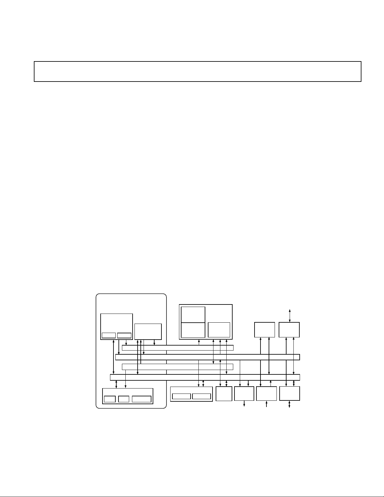
FUNCTIONAL BLOCK DIAGRAM
ADSP-2100 BASE
ARCHITECTURE
DATA
ADDRESS
GENERATORS
DAG 2
DAG 1
ARITHMETIC UNITS
MAC
ALU
PROGRAM
SEQUENCER
PROGRAM MEMORY ADDRESS
DATA MEMORY ADDRESS
PROGRAM MEMORY DATA
DATA MEMORY DATA
SHIFTER
PROGRAM
2K 24
PROGRAM
2K 24
SERIAL PORTS
SPORT 0
REV. B
Information furnished by Analog Devices is believed to be accurate and
reliable. However, no responsibility is assumed by Analog Devices for its
use, nor for any infringements of patents or other rights of third parties
which may result from its use. No license is granted by implication or
otherwise under any patent or patent rights of Analog Devices.
(Continued on page 7)
ROM
RAM
MEMORY
AUX
PWM
WATCH-
DOG
TIMER
7
ANALOG
INPUTS
24-BIT
PIO
16-BIT
3-PHASE
PWM
DATA
RAM
1K 16
2 8 BIT
SPORT 1
TIMER
One Technology Way, P.O. Box 9106, Norwood, MA 02062-9106, U.S.A.
Tel: 781/329-4700 World Wide Web Site: http://www.analog.com
Fax: 781/326-8703 © Analog Devices, Inc., 2000

ADMC331–SPECIFICATIONS
(VDD = +5 V 10%, GND = SGND = 0 V, TA = –40C to +85C, unless otherwise noted)
Parameter Min Typ Max Units Conditions/Comments
ANALOG-TO-DIGITAL CONVERTER Charging Capacitor = 1000 pF
2.5 kHz Sample Frequency
Signal Input 0.3 3.3
Resolution 12
1
2
V
Bits No Missing Codes
Converter Linearity 2 12 LSBs
Zero Offset 5 50 mV
Channel-to-Channel Comparator Match 22 mV
Comparator Delay 600 ns
Current Source 10.16 12.7 15.24 µA
Current Source Linearity 2 %
ELECTRICAL CHARACTERISTICS
V
Logic Low 0.8 V
IL
Logic High 2 V
V
IH
V
Low Level Output Voltage 0.4 V IOL = 2 mA
OL
V
Low Level Output Voltage (XTAL) 0.5 V IOL = 2 mA
OL
High Level Output Voltage 4 V I
V
OH
I
Low Level Input Current –10 µAV
IL
I
High Level Input Current 10 µAV
IH
I
Hi-Level PWMTRIP, PIO0–PIO23 Current 100 µA@ V
IH
I
Hi-Level PWMPOL/PWMSR Current 10 µA@ V
IH
I
Lo-Level PWMTRIP, PIO0–PIO23 Current 10 µA@ V
IL
Lo-Level PWMPOL/PWMSR Current 100 µA@ V
I
IL
I
Supply Current (Dynamic) 120 mA 13 MHz DSP Clock
DD
I
Supply Current (Idle) 60 mA 13 MHz DSP Clock
DD
= 0.5 mA
OH
= 0 V
IN
= V
IN
DD
= max, VIN = VDD max
DD
= max, VIN = VDD max
DD
= max, VIN = 0 V
DD
= max, VIN = 0 V
DD
REFERENCE VOLTAGE OUTPUT
Voltage Level 2.2 2.55 2.9 V 100 µA Load
Output Voltage Change T
MIN
to T
MAX
20 mV
16-BIT PWM TIMER
Counter Resolution 16 Bits
Edge Resolution (Single Update Mode) 76.9 ns 13 MHz CLKIN
Edge Resolution (Double Update Mode) 38.5 ns 13 MHz CLKIN
Programmable Deadtime Range 0 78 µs 13 MHz CLKIN
Programmable Deadtime Increments 76.9 ns 13 MHz CLKIN
Programmable Pulse Deletion Range 0 78 µs 13 MHz CLKIN
Programmable Pulse Deletion Increments 76.9 ns 13 MHz CLKIN
PWM Frequency Range 0.198 kHz 13 MHz CLKIN
PWMSYNC Pulsewidth (T
) 0.077 9.8 µs 13 MHz CLKIN
CRST
Gate Drive Chop Frequency Range 0.02 6.5 MHz 13 MHz CLKIN
AUXILIARY PWM TIMERS
Resolution 8 Bits
PWM Frequency 0.051 6.5 MHz 13 MHz CLKIN
NOTES
1
Signal input max V = 3.5 V if VDD = 5 V ± 5%.
2
Resolution varies with PWM switching frequency (13 MHz Clock in Double Update mode), 50.7 kHz = 9 bits, 6.3 kHz = 12 bits.
Specifications subject to change without notice.
–2–
REV. B
ADMC331
CLKIN
CLKOUT
t
CKOH
t
CKI
t
CKIH
t
CKH
t
CKL
t
CKIL
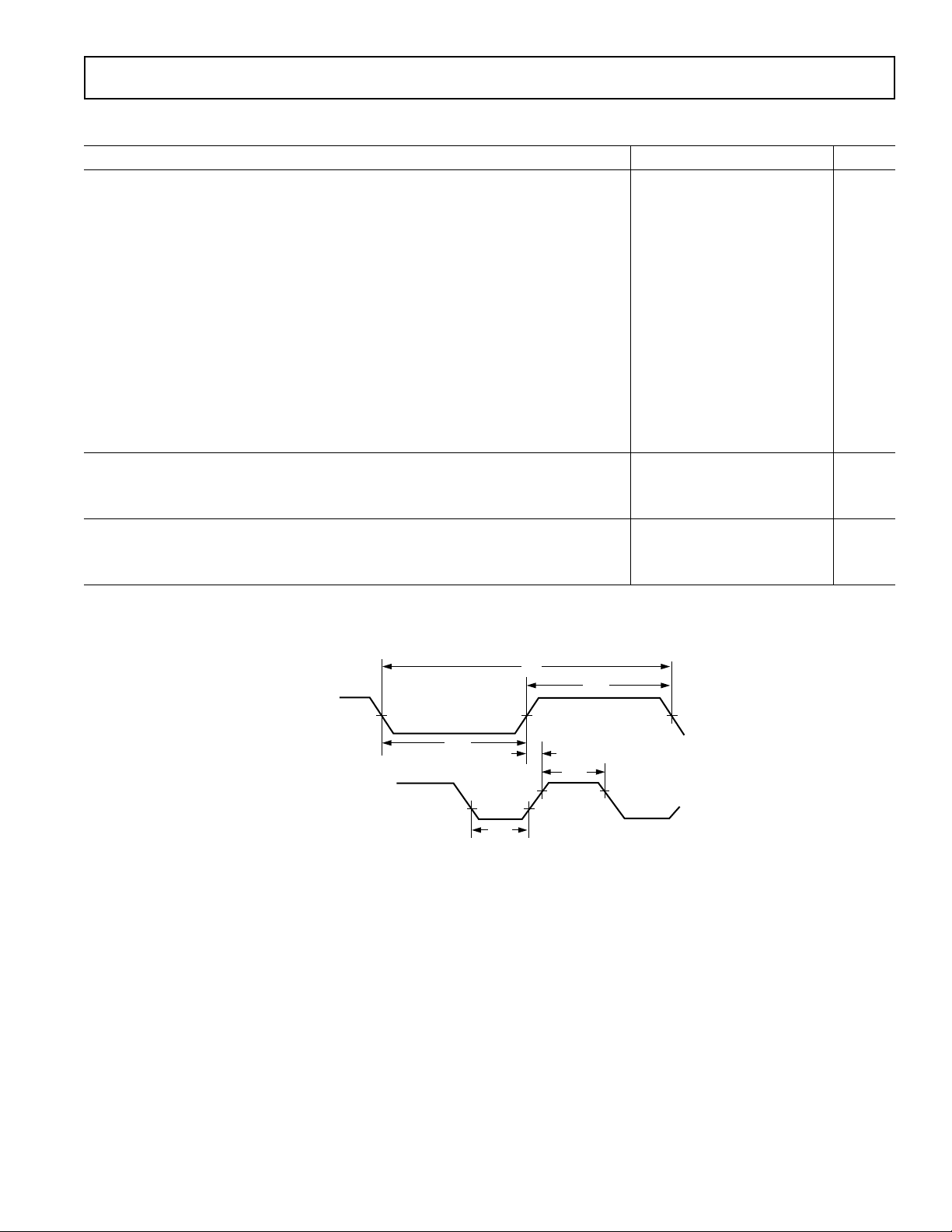
TIMING PARAMETERS
Parameter Min Max Unit
Clock Signals
tCK is defined as 0.5 t
to half the instruction rate; a 13 MHz input clock (which is equivalent to 76.9 ns)
yields a 38.5 ns processor cycle (equivalent to 26 MHz). t
of 0.5 t
period should be substituted for all relevant timing parameters to obtain
CKI
specification value.
Example: t
= 0.5 tCK – 10 ns = 0.5 (38.5 ns) – 10 ns = 9.25 ns.
CKH
Timing Requirements:
t
CKI
t
CKIL
t
CKIH
Switching Characteristics:
t
CKL
t
CKH
t
CKOH
Control Signals
Timing Requirement:
t
RSP
PWM Shutdown Signals
Timing Requirement:
t
PWMTPW
NOTE
1
Applies after power-up sequence is complete. Internal phase lock loop requires no more than 2000 CLKIN cycles assuming stable CLKIN (not including crystal
oscillator start-up time).
. The ADMC331 uses an input clock with a frequency equal
CKI
values within the range
CK
CLKIN Period 76.9 150 ns
CLKIN Width Low 20 ns
CLKIN Width High 20 ns
CLKOUT Width Low 0.5 tCK – 10 ns
CLKOUT Width High 0.5 tCK – 10 ns
CLKIN High to CLKOUT High 0 20 ns
RESET Width Low 5 t
PWMTRIP Width Low 2 t
CK
CK
1
ns
ns
Figure 1. Clock Signals
–3–REV. B
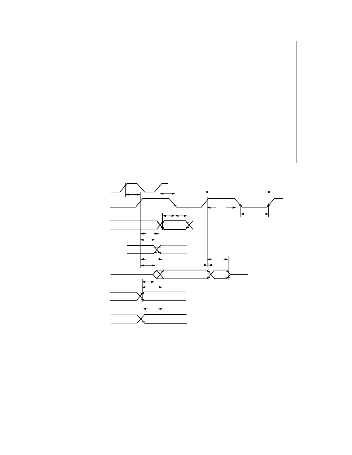
ADMC331
Parameter Min Max Unit
Serial Ports
Timing Requirements:
t
SCK
t
SCS
t
SCH
t
SCP
Switching Characteristics:
t
CC
t
SCDE
t
SCDV
t
RH
t
RD
t
SCDH
t
SCDD
t
TDE
t
TDV
t
RDV
SCLK Period 100 ns
DR/TFS/RFS Setup before SCLK Low 15 ns
DR/TFS/RFS Hold after SCLK Low 20 ns
SCLKIN Width 40 ns
CLKOUT High to SCLK
OUT
0.25 t
CK
0.25 tCK + 20 ns
SCLK High to DT Enable 0 ns
SCLK High to DT Valid 30 ns
TFS/RFS
TFS/RFS
Hold after SCLK High 0 ns
OUT
Delay from SCLK High 30 ns
OUT
DT Hold after SCLK High 0 ns
SCLK High to DT Disable 30 ns
TFS (Alt) to DT Enable 0 ns
TFS (Alt) to DT Valid 25 ns
RFS (Multichannel, Frame Delay Zero) to DT Valid 30 ns
CLKOUT
SCLK
DR
RFS
TFS
RFS
OUT
TFS
OUT
DT
TFS
(ALTERNATE
FRAME MODE)
(MULTICHANNEL MODE,
FRAME DELAY 0 [MFD = 0])
RFS
t
CC
IN
IN
t
t
RH
SCDE
t
t
TDE
t
RD
SCDV
t
t
TDV
RDV
t
CC
t
t
SCDD
t
t
SCH
SCS
t
SCDH
SCP
t
SCK
t
SCP
Figure 2. Serial Ports
–4–
REV. B

ADMC331
WARNING!
ESD SENSITIVE DEVICE
ABSOLUTE MAXIMUM RATINGS*
Supply Voltage (VDD) . . . . . . . . . . . . . . . . . . –0.3 V to +7.0 V
Supply Voltage (AV
Input Voltage . . . . . . . . . . . . . . . . . . . . –0.3 V to V
Output Voltage Swing . . . . . . . . . . . . . .–0.3 V to V
) . . . . . . . . . . . . . . . . .–0.3 V to +7.0 V
DD
+ 0.3 V
DD
+ 0.3 V
DD
*Stresses greater than those listed above may cause permanent damage to the
device. These are stress ratings only; functional operation of the device at these
or any other conditions greater than those indicated in the operational sections of
this specification is not implied. Exposure to absolute maximum rating conditions
for extended periods may affect device reliability.
Operating Temperature Range (Ambient) . . . –40°C to +85°C
Storage Temperature Range . . . . . . . . . . . . –65°C to +150°C
Lead Temperature (5 sec) . . . . . . . . . . . . . . . . . . . . . .+280°C
ORDERING GUIDE
Temperature Instruction Package Package
Model Range Rate Description Option
ADMC331BST –40°C to +85°C 26 MHz 80-Lead Plastic Thin Quad Flatpack (TQFP) ST-80
ADMC331-ADVEVALKIT Development Tool Kit
ADMC331-PB Evaluation/Processor Board
CAUTION
ESD (electrostatic discharge) sensitive device. Electrostatic charges as high as 4000 V readily
accumulate on the human body and test equipment and can discharge without detection.
Although the ADMC331 features proprietary ESD protection circuitry, permanent damage may
occur on devices subjected to high-energy electrostatic discharges. Therefore, proper ESD
precautions are recommended to avoid performance degradation or loss of functionality.
–5–REV. B
ADMC331
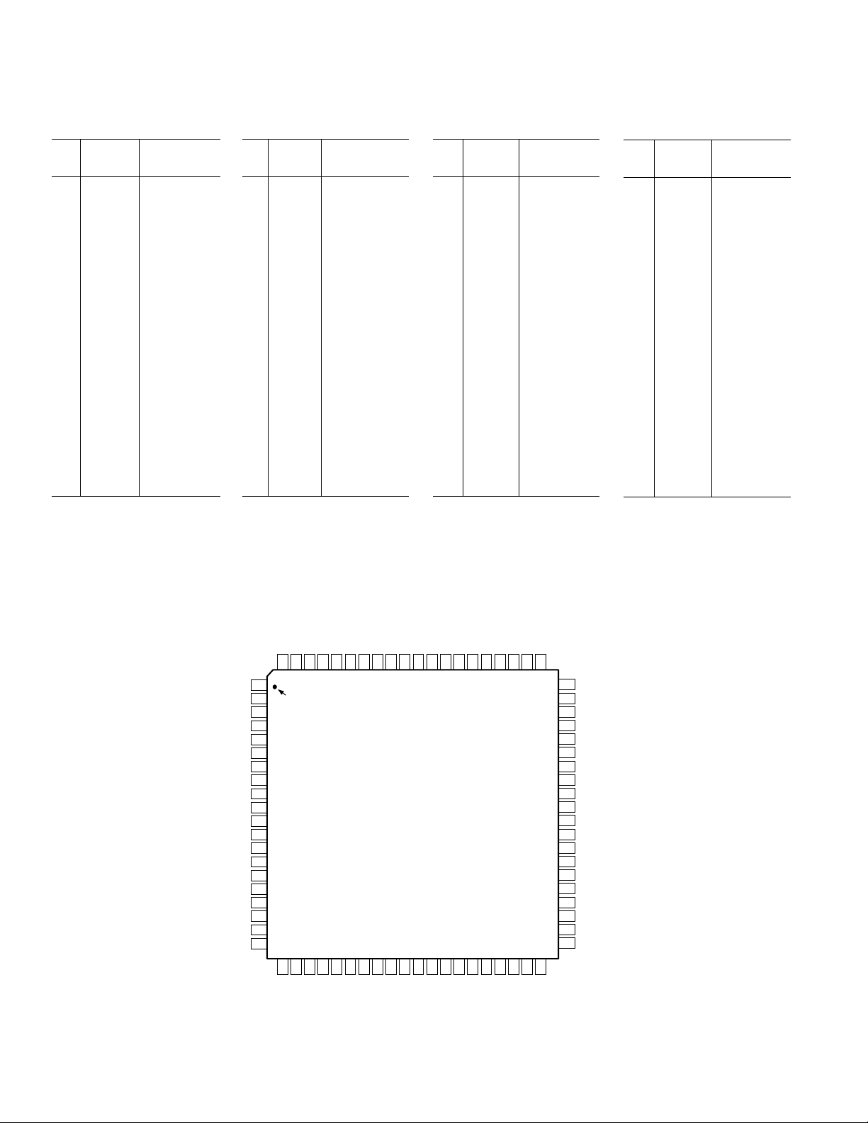
PIN FUNCTION DESCRIPTIONS
Pin Pin Pin
No. Type Name
1 O/P VREF
2 SUP AV
DD
3 GND GND
4 BIDIR PIO9
5 BIDIR PIO8
6 BIDIR PIO7
7 BIDIR PIO6
8 BIDIR PIO5
9 BIDIR PIO4
10 BIDIR PIO3
11 BIDIR PIO2
12 BIDIR PIO1
13 BIDIR PIO0
14 O/P AUX1
15 O/P AUX0
16 BIDIR PIO10
17 BIDIR PIO11
18 SUP V
DD
19 I/P PWMTRIP
20 GND GND
Pin Pin Pin
No. Type Name
21 SUP V
DD
22 GND GND
23 BIDIR PIO12
24 BIDIR PIO13
25 O/P PWMSYNC
26 O/P CL
27 O/P CH
28 O/P BL
29 O/P BH
30 O/P AL
31 O/P AH
32 BIDIR PIO14
33 BIDIR PIO15
34 BIDIR PIO16
35 SUP V
DD
36 GND GND
37 BIDIR PIO17
38 GND GND
39 BIDIR PIO18
40 GND GND
PIN CONFIGURATION
80-Lead Plastic Thin Quad Flatpack (TQFP)
Pin Pin Pin
No. Type Name
41 GND GND
42 GND GND
43 O/P XTAL
44 I/P CLKIN
45 I/P PWMPOL
46 I/P RESET
47 GND GND
48 SUP V
49 BIDIR PIO19
50 BIDIR PIO20
51 O/P CLKOUT
52 GND GND
53 O/P DT1
54 BIDIR TFS1
55 BIDIR RFS1/SROM
56 I/P DR1A
57 I/P DR1B
58 BIDIR SCLK1
59 O/P DT0
60 I/P PWMSR
(ST-80)
DD
Pin Pin Pin
No. Type Name
61 BIDIR TFS0
62 BIDIR RFS0
63 I/P DR0
64 BIDIR SCLK0
65 BIDIR PIO21
66 BIDIR PIO22
67 BIDIR PIO23
68 SUP V
DD
69 GND GND
70 GND AGND
71 I/P CAPIN
72 O/P ICONST
73 GND SGND
74 I/P V1
75 I/P V2
76 I/P V3
77 I/P VAUX0
78 I/P VAUX1
79 I/P VAUX2
80 I/P VAUX3
VREF
AV
GND
PIO9
PIO8
PIO7
PIO6
PIO5
PIO4
PIO3
PIO2
PIO1
PIO0
AUX1
AUX0
PIO10
PIO11
V
PWMTRIP
GND
VAUX3
80
7978777675
1
PIN 1
2
DD
DD
IDENTIFIER
3
4
5
6
7
8
9
10
11
12
13
14
15
16
17
18
19
20
21
22
23
DD
V
GND
PIO12
25
24
PIO13
PWMSYNC
V2
26
CL
V1
74
27
CH
CAPIN
ICONST
SGND
73
727170
ADMC331
TOP VIEW
(Not to Scale)
30
28
29
AL
BL
BH
V3
VAUX0
VAUX1
VAUX2
DD
V
GND
AGND
31
AH
PIO22
PIO23
69686766656463
32
35
33
34
DD
V
PIO16
PIO15
PIO14
PIO21
36
GND
SCLK0
37
38
GND
PIO17
DR0
RFS0
62
39
GND
PIO18
TFS0
61
40
60
PWMSR
DT0
59
SCLK1
58
DR1B
57
DR1A
56
55
RFS1/ SROM
TFS1
54
53
DT1
GND
52
51
CLKOUT
50
PIO20
PIO19
49
V
48
DD
GND
47
46
RESET
45
PWMPOL
CLKIN
44
XTAL
43
GND
42
GND
41
–6–
REV. B

ADMC331
(Continued from page 1)
Two Programmable Operational Modes
Independent Mode
Offset Mode
16-Bit Watchdog Timer
Programmable 16-Bit Internal Timer with Prescaler
Two Double Buffered Synchronous Serial Ports
Four Boot Load Protocols via SPORT1
2
PROM/SROM Booting
E
UART Booting (SCI Compatible) with Autobaud
Feature
Synchronous Master Booting with Autobaud Feature
Synchronous Slave Booting with Autobaud Feature
Debugger Interface via SPORT1 with Autobaud (UART
and Synchronous Supported)
ROM Utilities
Full Debugger for Program Development
Preprogrammed Math Functions
Preprogrammed Motor Control Functions—Vector
Transformations
80-Lead TQFP Package
Industrial Temperature Range –40C to +85C
GENERAL DESCRIPTION
The ADMC331 is a low cost, single-chip DSP-based controller,
suitable for ac induction motors, permanent magnet synchronous motors, brushless dc motors, and switched reluctance
motors. The ADMC331 integrates a 26 MIPS, fixed-point DSP
core with a complete set of motor control peripherals that permits fast, efficient development of motor controllers.
The DSP core of the ADMC331 is the ADSP-2171, which is
completely code compatible with the ADSP-2100 DSP family
and combines three computational units, data address generators and a program sequencer. The computational units comprise an ALU, a multiplier/accumulator (MAC) and a barrel
shifter. The ADSP-2171 adds new instructions for bit manipulation, multiplication (X squared), biased rounding and global
interrupt masking. In addition, two flexible, double-buffered,
bidirectional, synchronous serial ports are included in the
ADMC331.
The ADMC331 provides 2K × 24-bit program memory RAM,
2K × 24-bit program memory ROM and 1K × 16-bit data
memory RAM. The program and data memory RAM can be
boot loaded through the serial port from a Serial ROM (SROM),
E2PROM, asynchronous (UART) connection or synchronous
connection. The program memory ROM includes a monitor
that adds software debugging features through the serial port. In
addition, a number of preprogrammed mathematical and motor
control functions are included in the program memory ROM.
The motor control peripherals of the ADMC331 include a
16-bit center-based PWM generation unit that can be used to
produce high accuracy PWM signals with minimal processor
overhead and seven analog input channels. The device also
contains two auxiliary 8-bit PWM channels, a 16-bit watchdog timer and expanded capability through the serial ports
and 24-bit digital I/O ports.
–7–REV. B
ADMC331
DATA
ADDRESS
GENERATOR
#1
INPUT REGS
ALU
OUTPUT REGS
DATA
ADDRESS
GENERATOR
#2
INPUT REGS
OUTPUT REGS
MAC
INSTRUCTION
PROGRAM
SEQUENCER
16
R BUS
REGISTER
OUTPUT REGS
14
14
24
BUS
EXCHANGE
16
INPUT REGS
SHIFTER
PM ROM
2K 24
PM RAM
2K 24
CONTROL
LOGIC
PMA BUS
DMA BUS
PMD BUS
DMD BUS
TRANSMIT REG
RECEIVE REG
Figure 3. DSP Core Block Diagram
SERIAL
PORT 0
5
DM RAM
1K 16
COMPANDING
CIRCUITRY
TRANSMIT REG
RECEIVE REG
SERIAL
PORT 1
6
TIMER
DSP CORE ARCHITECTURE OVERVIEW
Figure 3 is an overall block diagram of the DSP core of the
ADMC331, which is based on the fixed-point ADSP-2171. The
flexible architecture and comprehensive instruction set of the
ADSP-2171 allows the processor to perform multiple operations
in parallel. In one processor cycle (38.5 ns with a 13 MHz
CLKIN) the DSP core can:
• Generate the next program address.
• Fetch the next instruction.
• Perform one or two data moves.
• Update one or two data address pointers.
• Perform a computational operation.
This all takes place while the processor continues to:
• Receive and transmit through the serial ports.
• Decrement the interval timer.
• Generate three-phase PWM waveforms for a power inverter.
• Generate two signals using the 8-bit auxiliary PWM timers.
• Acquire four analog signals.
• Decrement the watchdog timer.
The processor contains three independent computational units:
the arithmetic and logic unit (ALU), the multiplier/accumulator
(MAC) and the shifter. The computational units process 16-bit
data directly and have provisions to support multiprecision computations. The ALU performs a standard set of arithmetic and
logic operations; division primitives are also supported. The
MAC performs single-cycle multiply, multiply/add, multiply/
subtract operations with 40 bits of accumulation. The shifter
performs logical and arithmetic shifts, normalization, denormalization
and derive exponent operations. The shifter can be used to efficiently implement numeric format control including floatingpoint representations.
The internal result (R) bus directly connects the computational
units so that the output of any unit may be the input of any unit
on the next cycle.
A powerful program sequencer and two dedicated data address
generators ensure efficient delivery of operands to these computational units. The sequencer supports conditional jumps and
subroutine calls and returns in a single cycle. With internal loop
counters and loop stacks, the ADMC331 executes looped code
with zero overhead; no explicit jump instructions are required
to maintain the loop.
Two data address generators (DAGs) provide addresses for
simultaneous dual operand fetches from data memory and
program memory. Each DAG maintains and updates four address pointers (I registers). Whenever the pointer is used to
access data (indirect addressing), it is post-modified by the
value in one of four modify (M registers). A length value may
be associated with each pointer (L registers) to implement automatic modulo addressing for circular buffers. The circular buffering feature is also used by the serial ports for automatic data
transfers to and from on-chip memory. DAG1 generates only
data memory address but provides an optional bit-reversal
capability. DAG2 may generate either program or data memory
addresses, but has no bit-reversal capability.
Efficient data transfer is achieved with the use of five internal
buses:
• Program Memory Address (PMA) Bus
• Program Memory Data (PMD) Bus
• Data Memory Address (DMA) Bus
• Data Memory Data (DMD) Bus
• Result (R) Bus
–8–
REV. B

ADMC331
Program memory can store both instructions and data, permitting the ADMC331 to fetch two operands in a single cycle—
one from program memory and one from data memory. The
ADMC331 can fetch an operand from on-chip program memory
and the next instruction in the same cycle.
The ADMC331 writes data from its 16-bit registers to the 24-bit
program memory using the PX register to provide the lower
eight bits. When it reads data (not instructions) from 24-bit
program memory to a 16-bit data register, the lower eight bits
are placed in the PX register.
The ADMC331 can respond to a number of distinct DSP core
and peripheral interrupts. The DSP core interrupts include
serial port receive and transmit interrupts, timer interrupts,
software interrupts and external interrupts. The motor control
peripherals also produce interrupts to the DSP core.
The two serial ports (SPORTs) provide a complete synchronous
serial interface with optional companding in hardware and a
wide variety of framed and unframed data transmit and receive
modes of operation. Each SPORT can generate an internal
programmable serial clock or accept an external serial clock.
Boot loading of both the program and data memory RAM of the
ADMC331 is through the serial port SPORT1.
A programmable interval counter is also included in the DSP
core and can be used to generate periodic interrupts. A 16-bit
count register (TCOUNT) is decremented every n processor
cycle, where n–1 is a scaling value stored in the 8-bit TSCALE
register. When the value of the counter reaches zero, an interrupt is
generated and the count register is reloaded from a 16-bit period register (TPERIOD).
The ADMC331 instruction set provides flexible data moves and
multifunction (one or two data moves with a computation) instructions. Each instruction is executed in a single 38.5 ns processor
cycle (for a 13 MHz CLKIN). The ADMC331 assembly language uses an algebraic syntax for ease of coding and readability. A comprehensive set of development tools support program
development. For further information on the DSP core, refer to
the ADSP-2100 Family User’s Manual, Third Edition, with par-
ticular reference to the ADSP-2171.
Serial Ports
The ADMC331 incorporates two complete synchronous serial
ports (SPORT0 and SPORT1) for serial communication and
multiprocessor communication. Following is a brief list of capabilities of the ADMC331 SPORTs. Refer to the ADSP-2100
Family User’s Manual, Third Edition, for further details.
• SPORTs are bidirectional and have a separate, double-buffered
transmit and receive section.
• SPORTs can use an external serial clock or generate their
own serial clock internally.
• SPORTs have independent framing for the receive and transmit sections. Sections run in a frameless mode or with frame
synchronization signals internally or externally generated. Frame
synchronization signals are active high or inverted, with either of
two pulsewidths and timings.
• SPORTs support serial data word lengths from 3 bits to 16
bits and provide optional A-law and µ-law companding ac-
cording to ITU (formerly CCITT) recommendation G.711.
• SPORT receive and transmit sections can generate unique
interrupts on completing a data word transfer.
• SPORTs can receive and transmit an entire circular buffer of
data with only one overhead cycle per data word. An interrupt
is generated after a data buffer transfer.
• SPORT0 has a multichannel interface to selectively receive
and transmit a 24-word or 32-word, time-division multiplexed, serial bitstream.
• SPORT1 can be configured to have two external interrupts
(IRQ0 and IRQ1), and the Flag In and Flag Out signals. The
internally generated serial clock may still be used in this configuration.
• SPORT1 is the default input for program and data memory
boot loading. The RFS1 pin can be configured internal to the
ADMC331 as an SROM/E
• SPORT1 has two data receive pins (DR1A and DR1B). The
DR1A pin is intended for synchronous boot loading from the
external SROM/E
data receive pin for boot loading from an external asynchronous (UART) connection (SCI compatible), an external
synchronous connection as the data receive pin for an external
device communicating over the debugger interface, or as the
data receive pin for a general purpose SPORT after booting.
These two pins are internally multiplexed onto the one DR1
port of the SPORT. The particular data receive pin selected is
determined by a bit in the MODECTRL register.
2
PROM. The DR1B pin can be used as the
2
PROM reset signal.
–9–REV. B

ADMC331
PIN FUNCTION DESCRIPTION
The ADMC331 is available in an 80-lead TQFP package. Table I
contains the pin descriptions.
Table I. Pin List
Pin #
Group of Input/
Name Pins Output Function
RESET 1 I/P Processor Reset Input.
SPORT0 5 I/P, O/P Serial Port 0 Pins (TFS0, RFS0,
DT0, DR0, SCLK0).
SPORT1 6 I/P, O/P Serial Port 1 Pins (TFS1, RFS1,
DT1, DR1A, DR1B, SCLK1).
CLKOUT 1 O/P Processor Clock Output.
CLKIN, XTAL 2 I/P, O/P External Clock or Quartz Crystal
Connection Point.
PIO0–PIO23 24 I/P, O/P Digital I/O Port Pins.
AUX0–AUX1 2 O/P Auxiliary PWM Outputs.
AH–CL 6 O/P PWM Outputs.
PWMTRIP 1 I/P PWM Trip Signal.
PWMPOL 1 I/P PWM Polarity Pin.
PWMSYNC 1 O/P PWM Synchronization Pin.
PWMSR 1 I/P Switch Reluctance Mode Pin.
V1–V3, 3 I/P Analog Inputs.
VAUX0–VAUX3 4 I/P Auxiliary Analog Input
CAPIN 1 I/P ADC Capacitor Input.
ICONST 1 O/P ADC Constant Current Source.
VREF 1 O/P Voltage Reference Output.
AV
DD
AGND 1 Analog Ground.
SGND 1 Analog Signal Ground
V
DD
GND 11
INTERRUPT OVERVIEW
1 Analog Power Supply.
5 Digital Power Supply.
Digital Ground.
The ADMC331 can respond to 34 different interrupt sources
with minimal overhead, 8 of which are internal DSP core
interrupts and 26 interrupts from the motor control peripherals.
The 8 DSP core interrupts are SPORT0 receive and transmit,
SPORT1 receive (or IRQ0) and transmit (or IRQ1), the internal
timer and two software interrupts. The motor control peripheral
interrupts are the 24 peripheral I/Os and two from the PWM
(PWMSYNC pulse and PWMTRIP). All motor control interrupts are multiplexed into the DSP core through the peripheral
IRQ2 interrupt. The interrupts are internally prioritized and individually maskable. A detailed description of the entire interrupt system of the ADMC331 is given later, following a more
detailed description of each peripheral block.
Memory Map
The ADMC331 has two distinct memory types: program
memory and data memory. In general, program memory contains
user code and coefficients, while the data memory is used to store
variables and data during program execution. Both program
memory RAM and ROM are provided on the ADMC331. Program memory RAM is arranged as one contiguous 2K × 24-bit
block, starting at address 0x0000. Program memory ROM is
located at address 0x0800. Data memory is arranged as a 1K ×
16-bit block starting at address 0x3800. The motor control
peripherals are memory mapped into a region of the data
memory space starting at 0x2000. The complete program and
data memory maps are given in Tables II and III, respectively.
Table II. Program Memory Map
Memory
Address Range Type Function
0x0000–0x002F RAM Interrupt Vector Table
0x0030–0x071F RAM User Program Space
0x0720–0x07EC RAM Reserved by Debugger
0x07ED–0x07FF RAM Reserved by Monitor
0x0800–0x0DEC ROM ROM Monitor
0x0DED–0x0FEA ROM ROM Math and Motor
Control Utilities
0x0FEB–0x0FFF ROM Reserved
Table III. Data Memory Map
Memory
Address Range Type Function
0x0000–0x1FFF Reserved
0x2000–0x20FF Memory Mapped Registers
0x2100–0x37FF Reserved
0x3800–0x3B5F RAM User Data Space
0x3B60–0x3BFF RAM Reserved by Monitor
0x3C00–0x3FFF Memory Mapped Registers
ROM Code
The 2K × 24-bit block of program memory ROM starting at address 0x0800 contains a monitor function that is used to download
and execute user programs via the serial port. In addition, the
monitor function supports an interactive mode in which commands
are received and processed from a host. An example of such a host
is the Windows
®
-based Motion Control Debugger, which is part of
the software development system for the ADMC331. In the interactive mode, the host can access both the internal DSP and peripheral motor control registers of the ADMC331, read and write to
both program and data memory, implement breakpoints and perform single-step and run/halt operation as part of the program
debugging cycle.
In addition to the monitor function, the program memory ROM
contains a number of useful mathematical and motor control utilities that can be called as subroutines from the user code. A complete list of these ROM functions is given in Table IV. The start
address of the function in the program memory ROM is also given.
Refer to the ADMC331 DSP Motor Controller Developer’s Reference
Manual for more details of the ROM functions.
Windows is a registered trademark of Microsoft Corporation.
–10–
REV. B
ADMC331
Table IV. ROM Utilities
Utility Address Function
PER_RST 0x07F1 Reset Peripherals.
UMASK 0x0DED Limits Unsigned Value to
Given Range.
PUT_VECTOR 0x0DF4 Facilitates User Setup of
Vector Table.
SMASK 0x0E06 Limits Signed Value to Given
Range.
ADMC_COS 0x0E26 Cosine Function.
ADMC_SIN 0x0E2D Sine Function.
ARCTAN 0x0E43 Arctangent Function.
RECIPROCAL 0x0E65 Reciprocal (1/×) Function.
SQRT 0x0E7B Square Root Function.
LN 0x0EB5 Natural Logarithm Function.
LOG 0x0EB8 Logarithm (Base 10) Function.
FLTONE 0x0ED4 Fixed Pt. to Float Conversion.
FIXONE 0x0ED9 Float to Fixed Pt. Conversion.
FPA 0x0EDD Floating Pt. Addition.
FPS 0x0EEC Floating Pt. Subtraction.
FPM 0x0EFC Floating Pt. Multiplication.
FPD 0x0F05 Floating Pt. Division.
FPMACC 0x0F26 Floating Pt. Multiply/Accumulate.
PARK 0x0F48 Forward/Reverse Park
Transformation.
REV_CLARK 0x0F5C Reverse Clark Transformation.
FOR_CLARK 0x0F72 Forward Clark Transformation.
COS64 0x0F80 64 Pt. COS Table.
ONE_BY_X 0x0FCO 16 Pt. 1/× Table.
SDIVQINT 0x0FD0 Unsigned Single Precision
Division (Integer).
SDIVQ 0x0FD9 Unsigned Single Precision
Division (Fractional).
SYSTEM INTERFACE
Figure 4 shows a basic system configuration for the ADMC331,
with an external crystal and serial E
2
PROM for boot loading of
program and data memory RAM.
CLKOUT
ADMC331
RESET
XTAL
CLKIN
DR1A
SCLK1
RFS1/ SROM
13 MHz
DATA
CLK
RESET
SERIAL
2
E
PROM
Figure 4. Basic System Configuration
Clock Signals
The ADMC331 can be clocked by either a crystal or a TTLcompatible clock signal. The CLKIN input cannot be halted,
changed during operation nor operated below the specified
minimum frequency during normal operation. If an external
clock is used, it should be a TTL-compatible signal running at
half the instruction rate. The signal is connected to the CLKIN
pin of the ADMC331. In this mode, with an external clock
signal, the XTAL pin must be left unconnected. The ADMC331
uses an input clock with a frequency equal to half the instruction rate; a 13 MHz input clock yields a 38.5 ns processor cycle
(which is equivalent to 26 MHz). Normally, instructions are
executed in a single processor cycle. All device timing is
relative to the internal instruction rate, which is indicated by
the CLKOUT signal.
Because the ADMC331 includes an on-chip oscillator feedback
circuit, an external crystal may be used instead of a clock
source, as shown in Figure 4. The crystal should be connected
across the CLKIN and XTAL pins, with two capacitors as
shown in Figure 4. A parallel-resonant, fundamental frequency,
microprocessor-grade crystal should be used. A clock output
signal (CLKOUT) is generated by the processor at the processor’s
cycle rate of twice the input frequency. This output can be
enabled and disabled by the CLKODIS bit of the SPORT0
Autobuffer Control Register, DM[0x3FF3]. However, extreme
care must be exercised when using this bit since disabling
CLKOUT effectively disables all motor control peripherals,
except the watchdog timer.
Reset
The RESET signal initiates a master reset of the ADMC331.
The RESET signal must be asserted during the power-up sequence to assure proper initialization. RESET during initial
power-up must be held long enough to allow the internal clock
to stabilize. If RESET is activated any time after power-up, the
clock continues to run and does not require stabilization time.
The power-up sequence is defined as the total time required for
the crystal oscillator circuit to stabilize after a valid V
DD
is applied to the processor, and for the internal phase-locked loop
(PLL) to lock onto the specific crystal frequency. A minimum
of 2000 CLKIN cycles ensures that the PLL has locked, but
does not include the crystal oscillator start-up time. During this
power-up sequence, the RESET signal should be held low. On
any subsequent resets, the RESET signal must meet the minimum pulsewidth specification, t
RSP
.
If an RC circuit is used to generate the RESET signal, the use of
an external Schmitt trigger is recommended.
The master reset sets all internal stack pointers to the empty
stack condition, masks all interrupts, initializes DSP core registers and performs a full reset of all of the motor control peripherals. When the RESET line is released, the first instruction is
fetched from internal program memory ROM at location 0x0800.
The internal monitor code at this location then commences the
boot-loading sequence over the serial port, SPORT1. A software controlled full peripheral reset is achieved by toggling the
DSP FL2 flag from 1 to 0 to 1 again.
–11–REV. B

ADMC331
Boot Loading
On power-up or reset, the ADMC331 is configured so that
execution begins at the internal PM ROM at address 0x0800.
This starts execution of the internal monitor function that first
performs some initialization functions and copies a default interrupt vector table to addresses 0x0000–0x002F of program memory
RAM. The monitor next attempts to boot load from an external
SROM or E
2
PROM on SPORT1 using the three wire connec-
tion of Figure 4. The monitor program first toggles the RFS1/
SROM pin of the ADMC331 to reset the serial memory device.
If an SROM or E
2
PROM is connected to SPORT1, data is
clocked into the ADMC331 at a rate CLKOUT/20. Both program and data memory RAM can be loaded from the SROM or
2
PROM. After the boot load is complete, program execution
E
begins at address 0x0030. This is where the first instruction of
the user code should be placed.
If boot loading from an E
2
PROM is unsuccessful, the monitor
code reconfigures SPORT1 as a UART and attempts to receive
commands from an external device on this serial port. The
monitor then waits for a byte to be received over SPORT1,
locks onto the baud rate of the external device (autobaud feature) and takes in a header word that tells it with what type of
device it is communicating. There are six alternatives:
• A UART boot loader such as a Motorola 68HC11SCI port.
• A synchronous slave boot loader (the clock is external).
• A synchronous master boot loader (the ADMC331 provides the
clock).
• A UART debugger interface.
• A synchronous master debugger interface.
• A synchronous slave debugger interface.
With the debugger interface, the monitor enters an interactive
mode in which it processes commands received from the external device.
DSP Control Registers
The DSP core has a system control register, SYSCNTL, memory
mapped at DM (0x3FFF). SPORT0 is enabled when Bit 12 is
set, disabled when this bit is cleared. SPORT1 is enabled when
Bit 11 is set, disabled when this bit is cleared. SPORT1 is configured as a serial port when Bit 10 is set, or as flags and interrupt lines when this bit is cleared. For proper operation of the
ADMC331, all other bits in this register must be cleared (which
is their default).
The DSP core has a wait state control register, MEMWAIT,
memory mapped at DM (0x3FFE). For proper operation of the
ADMC331, this register must always contain the value 0x8000
(which is the default).
The configuration of both the SYSCNTL and MEMWAIT
registers of the ADMC331 is shown at the end of the data sheet.
THREE-PHASE PWM CONTROLLER
Overview
The PWM generator block of the ADMC331 is a flexible, programmable, three-phase PWM waveform generator that can be
programmed to generate the required switching patterns to drive
a three-phase voltage source inverter for ac induction (ACIM),
or permanent magnet synchronous (PMSM) or a switched or
variable reluctance (SRM) motor control. In addition, the
PWM block contains special functions that considerably simplify the generation of the required PWM switching patterns for
control of the electronically commutated motor (ECM) or
brushless dc motor (BDCM).
The PWM generator produces three pairs of PWM signals on
the six PWM output pins (AH, AL, BH, BL, CH and CL). The
six PWM output signals consist of three high side drive signals
(AH, BH and CH) and three low side drive signals (AL, BL and
CL). The polarity of the generated PWM signals may be
programmed by the PWMPOL pin, so that either active HI or
active LO PWM patterns can be produced by the ADMC331.
The switching frequency, dead time and minimum pulsewidths
of the generated PWM patterns are programmable using respectively the PWMTM, PWMDT and PWMPD registers. In addition, three duty cycle control registers (PWMCHA, PWMCHB
and PWMCHC) directly control the duty cycles of the three
pair of PWM signals.
When the PWMSR pin is pulled low, the PWM generator transforms the six PWM output signals into six waveforms for
switched reluctance gate drive signals. The low side PWM
signals from the three-phase timing unit assume permanently
ON states, independent of the value written to the duty-cycle
registers. The duty cycles of the high side PWM signals from the
timing unit are still determined by the three duty-cycle registers.
Each of the six PWM output signals can be enabled or disabled
by separate output enable bits of the PWMSEG register. In
addition, three control bits of the PWMSEG register permit
crossover of the two signals of a PWM pair for easy control of
ECM or BDCM. In crossover mode, the PWM signal destined
for the high side switch is diverted to the complementary low
side output and the signal destined for the low side switch is
diverted to the corresponding high side output signal.
In many applications, there is a need to provide an isolation
barrier in the gate-drive circuits that turn on the power devices
of the inverter. In general, there are two common isolation
techniques, optical isolation using opto-couplers, and transformer isolation using pulse transformers. The PWM controller
of the ADMC331 permits mixing of the output PWM signals
with a high frequency chopping signal to permit easy interface to
such pulse transformers. The features of this gate-drive chopping mode can be controlled by the PWMGATE register. There
is an 8-bit value within the PWMGATE register that directly controls the chopping frequency. In addition, high frequency chopping
can be independently enabled for the high side and the low side
outputs using separate control bits in the PWMGATE register.
The PWM generator is capable of operating in two distinct
modes, single update mode or double update mode. In single
update mode, the duty cycle values are programmable only once
per PWM period, so that the resultant PWM patterns are symmetrical about the midpoint of the PWM period. In the double
update mode, a second updating of the PWM duty cycle values
is implemented at the midpoint of the PWM period. In this
mode, it is possible to produce asymmetrical PWM patterns,
that produce lower harmonic distortion in three-phase PWM
inverters. This technique also permits the closed loop controller
to change the average voltage applied to the machine winding at
a faster rate and so permits fast closed loop bandwidths to be
achieved. The operating mode of the PWM block (single or
double update mode) is selected by a control bit in MODECTRL
register.
–12–
REV. B

ADMC331
PWM CONFIGURATION
REGISTERS
PWMTM (15 . . . 0)
PWMDT (9 . . . 0)
PWMPD (9 . . . 0)
PWMSYNCWT (7 . . . 0)
MODECTRL (6)
THREE-PHASE
PWM TIMING
CLK
PWMSYNC
TO INTERRUPT
CONTROLLER
PWMTRIP
PWM DUTY CYCLE
REGISTERS
PWMCHA (15 . . . 0)
PWMCHB (15 . . . 0)
PWMCHC (15 . . . 0)
PWMSEG PWMGATE
UNIT
SYNC
RESET
SWITCHED
RELUCTANCE
CONTROL
UNIT
SR
OR
OUTPUT
CONTROL
UNIT
SYNC
PWMSWT (0)
Figure 5. Overview of the PWM Controller of the ADMC331
CLK
GATE
DRIVE
UNIT
POL
AH
AL
BH
BL
CH
CL
CLKOUT
PWMSYNC
PWMPOL
PWMSR
PWMTRIP
The PWM generator of the ADMC331 also provides an output
pulse on the PWMSYNC pin that is synchronized to the PWM
switching frequency. In single update mode, a PWMSYNC
pulse is produced at the start of each PWM period. In double
update mode, an additional PWMSYNC pulse is produced at
the midpoint of each PWM period. The width of the PWMSYNC pulse is programmable through the PWMSYNCWT
register.
The PWM signals produced by the ADMC331 can be shut-off
in two different ways. Firstly there is a dedicated asynchronous
PWM shutdown pin, PWMTRIP, that when brought LO, instantaneously places all six PWM outputs in the OFF state (as
determined by the state of the PWMPOL pin). This hardware
shutdown mechanism is asynchronous so that the associated
PWM disable circuitry does not go through any clocked logic,
thereby ensuring correct PWM shutdown even in the event of a
loss of DSP clock. In addition to the hardware shutdown feature, the PWM system may be shutdown in software by writing
to the PWMSWT register.
Status information about the PWM system of the ADMC331 is
available to the user in the SYSSTAT register. In particular,
the state of the PWMTRIP, PWMPOL and PWMSR pins is
available, as well as a status bit that indicates whether operation
is in the first half or the second half of the PWM period.
A functional block diagram of the PWM controller is shown in
Figure 5. The generation of the six output PWM signals on
pins AH to CL is controlled by four important blocks:
• The Three-Phase PWM Timing Unit, which is the core of the
PWM controller, generates three pairs of complemented and
dead time adjusted center based PWM signals.
• The Switched Reluctance Control Unit transforms the threephase outputs into six PWM wave forms for switched reluctance gate drive signals.
• The Output Control Unit allows the redirection of the outputs of the Three-Phase Timing Unit for each channel to
either the high side or the low side output. In addition, the
Output Control Unit allows individual enabling/disabling of
each of the six PWM output signals.
• The GATE Drive Unit provides the correct polarity output
PWM signals based on the state of the PWMPOL pin. The
Gate Drive Unit also permits the generation of the high frequency chopping frequency and its subsequent mixing with
the PWM signals.
The PWM controller is driven by a clock at the same frequency
as the DSP instruction rate, CLKOUT, and is capable of generating two interrupts to the DSP core. One interrupt is generated on the occurrence of a PWMSYNC pulse and the other is
generated on the occurrence of any PWM shutdown action.
Three-Phase Timing Unit
The 16-bit three-phase timing unit is the core of the PWM
controller and produces three pair of pulsewidth modulated
signals with high resolution and minimal processor overhead.
The outputs of this timing unit are active LO such that a low
level is interpreted as a command to turn ON the associated
power device. There are four main configuration registers
(PWMTM, PWMDT, PWMPD and PWMSYNCWT) that
determine the fundamental characteristics of the PWM outputs.
In addition, the operating mode of the PWM (single or double
update mode) is selected by Bit 6 of the MODECTRL register.
–13–REV. B

ADMC331
These registers, in conjunction with the three 16-bit duty-cycle
registers (PWMCHA, PWMCHB and PWMCHC), control the
output of the three-phase timing unit.
PWM Switching Frequency, PWMTM Register
The PWM switching frequency is controlled by the 16-bit read/
write PWM period register, PWMTM. The fundamental timing
unit of the PWM controller is t
(DSP instruction rate).
CK
Therefore, for a 26 MHz CLKOUT, the fundamental time
increment is 38.5 ns. The value written to the PWMTM register is effectively the number of t
clock increments in half a
CK
PWM period. The required PWMTM value is a function of the
desired PWM switching frequency (f
f
PWMTM =
CLKOUT
2 × f
) and is given by:
PWM
f
CLKIN
=
f
PWM
PWM
Therefore, the PWM switching period, TS, can be written as:
TS= 2 × PWMTM × t
CK
For example, for a 26 MHz CLKOUT and a desired PWM
switching frequency of 10 kHz (TS = 100 µs), the correct value
to load into the PWMTM register is:
6
PWMTM =
26 ×10
2 ×10 ×10
= 1300
3
The largest value that can be written to the 16-bit PWMTM
register is 0xFFFF = 65,535 which corresponds to a minimum
PWM switching frequency of:
6
f
PWM,min
PWM Switching Dead Time, PWMDT Register
26 ×10
=
2 × 65,535
= 198.4 Hz
The second important parameter that must be set up in the
initial configuration of the PWM block is the switching dead
time. That is a short delay time introduced between turning off
one PWM signal (AH) and turning on the complementary signal, AL. This short time delay is introduced to permit the
power switch being turned off (AH in this case) to completely
recover its blocking capability before the complementary switch
is turned on. This time delay prevents a potentially destructive
short-circuit condition from developing across the dc link capacitor of a typical voltage source inverter.
The dead time is controlled by the 10-bit, read/write PWMDT
register. There is only one dead time register that controls the
dead time inserted into the three pairs of PWM output signals.
The dead time, T
, is related to the value in the PWMDT regis-
D
ter by:
TD= PWMTM × 2 × t
CK
Therefore, a PWMDT value of 0x00A (= 10), introduces a
769.2 ns delay between the turn-off on any PWM signal (AH)
and the turn-on of its complementary signal (AL). The amount
of the dead time can therefore be programmed in increments of
(or 76.92 ns for a 26 MHz CLKOUT). The PWMDT
2t
CK
register is a 10-bit register so that its maximum value is 0x3FF
(=1023) corresponding to a maximum programmed dead time
of:
T
= 1023 × 2 × tCK = 1023 × 2 × 38.46 × 10–9 = 78.69 µs
D,max
for a CLKOUT rate of 26 MHz. Obviously, the deadtime can
be programmed to be zero by writing 0 to the PWMDT register.
PWM Operating Mode, MODECTRL and SYSSTAT Registers
The PWM controller of the ADMC331 can operate in two
distinct modes: single update mode and double update mode.
The operating mode of the PWM controller is determined by
the state of Bit 6 of the MODECTRL register. If this bit is
cleared, the PWM operates in the single update mode. Setting
Bit 6 places the PWM in the double update mode. By default,
following either a peripheral reset or power on, Bit 6 of the
MODECTRL register is cleared so that the default operating
mode is in single update mode.
In single update mode, a single PWMSYNC pulse is produced
in each PWM period. The rising edge of this signal marks the
start of a new PWM cycle and is used to latch new values from
the PWM configuration registers (PWMTM, PWMDT, PWMPD
and PWMSYNCWT) and the PWM duty-cycle registers
(PWMCHA, PWMCHB and PWMCHC) into the three-phase
timing unit. In addition, the PWMSEG register is also latched
into the output control unit on the rising edge of the PWMSYNC
pulse. In effect, this means that the characteristics and resultant
duty cycles of the PWM signals can be updated only once per
PWM period at the start of each cycle. The result is that PWM
patterns that are symmetrical about the midpoint of the switching period are produced.
In double update mode, there is an additional PWMSYNC
pulse produced at the midpoint of each PWM period. The rising
edge of this new PWMSYNC pulse is again used to latch new
values of the PWM configuration registers, duty-cycle registers
and the PWMSEG register. As a result it is possible to alter
both the characteristics (switching frequency, dead time, minimum
pulsewidth and PWMSYNC pulsewidth) as well as the output
duty cycles at the midpoint of each PWM cycle. Consequently, it is
possible to produce PWM switching patterns that are no longer
symmetrical about the midpoint of the period (asymmetrical
PWM patterns).
In the double update mode, it may be necessary to know whether
operation at any point in time is in either the first half or the
second half of the PWM cycle. This information is provided by
Bit 3 of the SYSSTAT register, which is cleared during operation in the first half of each PWM period (between the rising
edge of the original PWMSYNC pulse and the rising edge of
the new PWMSYNC pulse introduced in double update mode).
Bit 3 of the SYSSTAT register is set during operation in the
second half of each PWM period. This status bit allows the user
to make a determination of the particular half-cycle during
implementation of the PWMSYNC interrupt service routine, if
required.
The advantage of the double update mode is that lower harmonic voltages can be produced by the PWM process and faster
control bandwidths are possible. However, for a given PWM
switching frequency, the PWMSYNC pulses occur at twice the
rate in the double update mode. Since new duty cycle values
must be computed in each PWMSYNC interrupt service routine, there is a larger computational burden on the DSP in the
double update mode.
–14–
REV. B

ADMC331
Width of the PWMSYNC Pulse, PWMSYNCWT Register
The PWM controller of the ADMC331 produces an output
PWM synchronization pulse at a rate equal to the PWM switching frequency in single update mode and at twice the PWM
frequency in the double update mode. This pulse is available
for external use at the PWMSYNC pin. The width of this
PWMSYNC pulse is programmable by the 8-bit read/write
PWMSYNCWT register. The width of the PWMSYNC pulse,
T
PWMSYNC
so that the width of the pulse is programmable from t
, is given by:
T
PWMSYNC
= tCK × (PWMSYNCWT + 1)
to 256 t
CK
CK
(corresponding to 38.5 ns to 9.84 µs for a CLKOUT rate of
26 MHz). Following a reset, the PWMSYNCWT register contains 0x27 (= 39) so that the default PWMSYNC width is
1.54 µs, again for a 26 MHz CLKOUT.
PWM Duty Cycles, PWMCHA, PWMCHB, PWMCHC
Registers
The duty cycles of the six PWM output signals on pins AH to
CL are controlled by the three 16-bit read/write duty-cycle
registers, PWMCHA, PWMCHB, and PWMCHC. The integer
value in the register PWMCHA controls the duty cycle of the
signals on AH and AL, in PWMCHB, controls the duty cycle of
the signals on BH and BL and in PWMCHC, controls the duty
cycle of the signals on CH and CL. The duty-cycle registers are
programmed in integer counts of the fundamental time unit,
, and define the desired on-time of the high side PWM signal
t
CK
produced by the three-phase timing unit over half the PWM
period. The switching signals produced by the three-phase
timing unit are also adjusted to incorporate the programmed
dead time value in the PWMDT register. The three-phase
timing unit produces active LO signals so that a LO level corresponds to a command to turn on the associated power device.
A typical pair of PWM outputs (in this case for AH and AL)
from the timing unit are shown in Figure 6 for operation in
single update mode. All illustrated time values indicate the
integer value in the associated register and can be converted to
time simply by multiplying by the fundamental time increment,
t
. Firstly, it is noted that the switching patterns are perfectly
CK
symmetrical about the midpoint of the switching period in
this single update mode since the same values of PWMCHA,
PWMTM and PWMDT are used to define the signals in both
half cycles of the period. It can be seen how the programmed
duty cycles are adjusted to incorporate the desired dead time
into the resultant pair of PWM signals. Clearly, the dead time is
incorporated by moving the switching instants of both PWM
signals (AH and AL) away from the instant set by the PWMCHA
register. Both switching edges are moved by an equal amount
(PWMDT × t
) to preserve the symmetrical output patterns.
CK
Also shown is the PWMSYNC pulse whose width is set by the
PWMSYNCWT register and Bit 3 of the SYSSTAT register,
which indicates whether operation is in the first or second half
cycle of the PWM period.
Obviously negative values of T
and TAL are not permitted and
AH
the minimum permissible value is zero, corresponding to a 0%
duty cycle. In a similar fashion, the maximum value is T
,
S
corresponding to a 100% duty cycle.
PWMCHA
AH
2 PWMDT
AL
PWMSYNC
SYSSTAT (3)
PWMTM PWMTM
PWMCHA
2 PWMDT
PWMSYNCWT + 1
Figure 6. Typical PWM Outputs of Three-Phase Timing
Unit in Single Update Mode (Active LO Waveforms)
The resultant on-times of the PWM signals in Figure 6 may be
written as:
T
= 2 × (PWMCHA – PWMDT) × t
AH
TAL = 2 × (PWMTM–PWMCHA–PWMDT) × t
CK
CK
and the corresponding duty cycles are:
T
PWMCHA – PWMDT
AH
=
T
S
T
PWMTM – PWMCHA – PWMDT
AL
=
T
S
PWMTM
PWMTM
dAL=
dAH=
The output signals from the timing unit for operation in double
update mode are shown in Figure 7. This illustrates a completely general case where the switching frequency, dead time
and duty cycle are all changed in the second half of the PWM
period. Of course, the same value for any or all of these quantities could be used in both halves of the PWM cycle. However,
it can be seen that there is no guarantee that symmetrical PWM
signal will be produced by the timing unit in this double update
mode. Additionally, it is seen that the dead time is inserted into
the PWM signals in the same way as in the single update mode.
AH
AL
PWMSYNC
SYSSTAT (3)
2 PWMDT
PWMSYNCWT1 + 1
PWMTM
PWMCHA
1
1
1
PWMCHA
2
2 PWMDT
PWMSYNCWT2 + 1
PWMTM
2
2
Figure 7. Typical PWM Outputs of Three-Phase Timing
Unit in Double Update Mode (Active LO Waveforms)
In general, the on-times of the PWM signals in double update
mode can be defined as:
TAH= PWMCHA1+ PWMCHA2− PWMDT1− PWMDT
()
TAL= ( PWMTM1+ PWMTM2– PWMCHA1– PWMCHA
– PWMDT1– PWMDT2) ×
t
CLK
× t
2
CK
2
–15–REV. B

ADMC331
where the subscript 1 refers to the value of that register during
the first half cycle and the subscript 2 refers to the value during
the second half cycle. The corresponding duty cycles are:
T
dAL=
dAL=
AH
T
S
T
AL
T
S
(PWMCHA
=
(PWMTM
=
+ PWMCHA2– PWMDT1– PWMDT2)
1
(PWMTM
+ PWMTM2– PWMCHA1– PWMCHA2– PWMDT1– PWMDT2)
1
+ PWMTM2)
1
(PWMTM
+ PWMTM2)
1
since for the completely general case in double update mode,
the switching period is given by:
TS= (PWMTM1+ PWMTM2)× t
CK
Again, the values of TAH and TAL are constrained to lie between
zero and T
.
S
Similar PWM signals to those illustrated in Figure 6 and Figure 7 can be produced on the BH, BL, CH and CL outputs by
programming the PWMCHB and PWMCHC registers in a manner identical to that described for PWMCHA.
The PWM controller does not produce any PWM outputs until
all of the PWMTM, PWMCHA, PWMCHB and PWMCHC
registers have been written to at least once. Once these registers
have been written, internal counting of the timers in the threephase timing unit is enabled.
Effective PWM Resolution
In single update mode, the same value of PWMCHA, PWMCHB and PWMCHC are used to define the on-times in both
half cycles of the PWM period. As a result, the effective resolution of the PWM generation process is 2 t
(or 76.9 ns for a
CK
26 MHz CLKOUT) since incrementing one of the duty-cycle
registers by 1 changes the resultant on-time of the associated
PWM signals by t
in each half period (or 2 tCK for the full
CK
period).
In double update mode, improved resolution is possible since
different values of the duty cycles registers are used to define the
on-times in both the first and second halves of the PWM period.
As a result, it is possible to adjust the on-time over the whole
period in increments of t
PWM resolution of t
. This corresponds to an effective
CK
in double update mode (or 38.5 ns for a
CK
26 MHz CLKOUT).
The achievable PWM switching frequency at a given PWM
resolution is tabulated in Table V.
Table V. Achievable PWM Resolution in Single and Double
Update Modes
Resolution Single Update Mode Double Update Mode
(Bit) PWM Frequency (kHz) PWM Frequency (kHz)
8 50.7 101.5
9 25.4 50.7
10 12.7 25.4
11 6.3 12.7
12 3.2 6.3
Minimum Pulsewidth, PWMPD Register
In many power converter switching applications, it is desirable
to eliminate PWM switching signals below a certain width. It
takes a certain finite time to both turn on and turn off modern
power semiconductor devices. Therefore, if the width of any of
the PWM signals goes below some minimum value, it may be
desirable to completely eliminate the PWM switching for that
particular cycle.
The allowable minimum on-time for any of the six PWM outputs over half a PWM period that can be produced by the PWM
controller may be programmed using the 10-bit read/write
PWMPD register. The minimum on-time is programmed in
increments of t
produced over any half PWM period, T
so that the minimum on-time that will be
CK
, is related to the
MIN
value in the PWMPD register by:
T
= PWMPD ×t
MIN
CK
so that a PWMPD value of 0x002 defines a permissible minimum on-time of 76.9 ns for a 26 MHz CLKOUT.
In each half cycle of the PWM, the timing unit checks the ontime of each of the six PWM signals. If any of the times are
found to be less than the value specified by the PWMPD register, the corresponding PWM signal is turned OFF for the entire
half period and its complementary signal is turned completely
ON.
Consider the example where PWMTM = 200, PWMCHA = 5,
PWMDT = 3, PWMPD = 10 with a CLKOUT of 26 MHz
and operation in single update mode. In this case, the PWM
switching frequency is 65 kHz and the dead time is 230 ns.
The permissible on-time of any PWM signal over one half of
any period is 384.6 ns. Clearly, for this example, the dead
time adjusted on-time of the AH signal over half a PWM
period is (5–3) × 38.5 ns = 77 ns. This is less than the permissible value, so the timing unit will output a completely OFF
(0% duty cycle) signal on AH. Additionally, the AL signal will
be turned ON for the entire half period (100% duty cycle).
Switched Reluctance Mode
The PWM block of the ADMC331 contains a switched reluctance mode that is controlled by the state of the PWMSR pin.
The switched reluctance (SR) mode is enabled by connecting
the PWMSR pin to GND. In this SR mode, the low side PWM
signals from the three-phase timing unit assume permanently
ON states, independent of the value written to the duty-cycle
registers. The duty cycles of the high side PWM signals from
the timing unit are still determined by the three duty-cycle registers. Using the crossover feature of the output control unit, it is
possible to divert the permanently ON PWM signals to either
the high side or the low side outputs. This mode is necessary
because in the typical power converter configuration for switched
or variable reluctance motors, the motor winding is connected
between the two power switches of a given inverter leg. Therefore, in order to build up current in the motor winding, it is
necessary to turn on both switches at the same time. Typical
active LO PWM signals during operation in SR mode are shown
in Figure 8 for operation in double update mode. It is clear that
the three low side signals (AL, BL and CL) are permanently ON
and the three high side signals are modulated so that the corresponding high side power switches are switched between the ON
and OFF states.
–16–
REV. B

ADMC331
AH
AL
BH
BL
CH
CL
PWMTM
PWMTM
PWMCHA
= PWMCHB
PWMCHA
= PWMCHB
2 PWMDT
2 PWMDT
PWMCHA
1
PWMCHA
2
2
PWMTM
2
2
AH
BH
CH
AL
BL
CL
PWMCHB
PWMCHC
PWMTM
1
1
1
PWMCHB
PWMCHC
Figure 8. Active LO PWM signals in SR Mode (PWMPOL =
PWMSR
= GND) for ADMC331 in double update mode.
The signals from the three-phase unit are not crossed over
(PWMSEG = 0) and the dead time is zero (PWMDT = 0).
The SR mode can only be enabled by connecting the PWMSR
pin to GND. There is no software means by which this mode
can be enabled. There is an internal pull-up resistor on the
PWMSR pin so that if this pin is left unconnected or becomes
disconnected the SR mode is disabled. Of course, the SR mode
is disabled when the PWMSR pin is tied to V
. The state of
DD
the PWMSR pin may be read from Bit 4 of the SYSSTAT
register.
Output Control Unit, PWMSEG Register
The operation of the Output Control Unit is controlled by the
9-bit read/write PWMSEG register that controls two distinct
features that are directly useful in the control of ECM or BDCM.
The PWMSEG register contains three crossover bits, one for
each pair of PWM outputs. Setting Bit 8 of the PWMSEG
register enables the crossover mode for the AH/AL pair of PWM
signals; setting Bit 7 enables crossover on the BH/BL pair of
PWM signals; setting Bit 6 enables crossover on the CH/CL
pair of PWM signals. If crossover mode is enabled for any pair
of PWM signals, the high side PWM signal from the timing unit
(i.e. AH) is diverted to the associated low side output of the
Output Control Unit so that the signal will ultimately appear at
the AL pin. Of course, the corresponding low side output of the
Timing Unit is also diverted to the complementary high side
output of the Output Control Unit so that the signal appears at
the AH pin. Following a reset, the three crossover bits are
cleared so that the crossover mode is disabled on all three pairs
of PWM signals.
The PWMSEG register also contains six bits (Bits 0 to 5) that
can be used to individually enable or disable each of the six
PWM outputs. The PWM signal of the AL pin is enabled by
setting Bit 5 of the PWMSEG register while Bit 4 controls AH,
Bit 3 controls BL, Bit 2 controls BH, Bit 1 controls CL and
Bit 0 controls the CH output. If the associated bit of the
PWMSEG register is set, then the corresponding PWM output
is disabled irrespective of the value of the corresponding duty
cycle register. This PWM output signal will remain in the OFF
state as long as the corresponding enable/disable bit of the
PWMSEG register is set. The implementation of this output
enable function is implemented after the crossover function.
Following a reset, all six enable bits of the PWMSEG register
are cleared so that all PWM outputs are enabled by default.
In a manner identical to the duty-cycle registers, the PWMSEG
is latched on the rising edge of the PWMSYNC signal so that
the changes to this register only become effective at the start of
each PWM cycle in single update mode. In double update mode,
the PWMSEG register can also be updated at the midpoint of
the PWM cycle.
In the control of an ECM, only two inverter legs are switched
at any time and often the high side device in one leg must be
switched ON at the same time as the low side driver in a second
leg. Therefore, by programming identical duty cycles values for
two PWM channels (i.e., PWMCHA = PWMCHB) and setting
Bit 7 of the PWMSEG register to crossover the BH/BL pair if
PWM signals, it is possible to turn ON the high side switch of
phase A and the low side switch of Phase B at the same time.
In the control of ECM, it is usual that the third inverter leg
(Phase C in this example) be permanently disabled for a number
of PWM cycles. This function is implemented by disabling both
the CH and CL PWM outputs by setting Bits 0 and 1 of the
PWMSEG register. This situation is illustrated in Figure 9
where it can be seen that both the AH and BL signals are identical, since PWMCHA = PWMCHB and the crossover bit for
Phase B is set. In addition, the other four signals (AL, BH, CH
and CL) have been disabled by setting the appropriate enable/
disable bits of the PWMSEG register. For the situation illustrated in Figure 9, the appropriate value for the PWMSEG
register is 0x00A7. In normal ECM operation, each inverter leg
is disabled for certain periods of time, so that the PWMSEG
register is changed based on the position of the rotor shaft
(motor commutation).
Figure 9. Example active LO PWM signals suitable for
ECM control, PWMCHA = PWMCHB, crossover BH/BL pair
and disable AL, BH, CH and CL outputs. Operation is in
single update mode.
Gate Drive Unit, PWMGATE Register
The Gate Drive Unit of the PWM controller adds features
that simplify the design of isolated gate drive circuits for
PWM inverters. If a transformer-coupled power device gate
driver amplifier is used, the active PWM signals must be
chopped at a high frequency. The 10-bit read/write PWMGATE
register allows the programming of this high frequency chopping
mode. The chopped active PWM signals may be required for
the high side drivers only, for the low side drivers only or for
both the high side and low side switches. Therefore, independent control of this mode for both high and low side switches is
–17–REV. B

ADMC331
included with two separate control bits in the PWMGATE
register.
Typical PWM output signals with high frequency chopping
enabled on both high side and low side signals are shown in
Figure 10. Chopping of the high side PWM outputs (AH, BH
and CH) is enabled by setting Bit 8 of the PWMGATE register.
Chopping of the low side PWM outputs (AL, BL and CL) is
enabled by setting Bit 9 of the PWMGATE register. The high
frequency chopping frequency is controlled by the 8-bit word
(GDCLK) placed in Bits 0 to 7 of the PWMGATE register.
The period of this high frequency carrier is:
T
= [4 × (GDCLK +1) ] ×t
CHOP
f
=
CHOP
[4 ×(GDCLK +1) ]
f
CLKOUT
CK
The GDCLK value may range from 0 to 255, corresponding to
a programmable chopping frequency rate from 25.39 kHz to
6.5 MHz for a 26 MHz CLKOUT rate. The gate drive features
must be programmed before operation of the PWM controller
and typically are not changed during normal operation of the
PWM controller. Following a reset, all bits of the PWMGATE
register are cleared so that high frequency chopping is disabled,
by default.
PWMCHA PWMCHA
2 PWMDT
[4 (GDCLK+1) tCK]
PWMTM
Figure 10. Typical Active LO PWM Signals with High Frequency Gate Chopping Enabled on Both High Side and
Low Side Switches
PWM Polarity Control, PWMPOL Pin
2 PWMDT
PWMTM
The polarity of the PWM signals produced at the output pins
AH to CL may be selected in hardware by the PWMPOL pin.
Connecting the PWMPOL pin to GND selects active LO PWM
outputs, such that a LO level is interpreted as a command to
turn on the associated power device. Conversely, connecting
to PWMPOL pin selects active HI PWM and the associ-
V
DD
ated power devices are turned ON by a HI level at the PWM
outputs. There is an internal pull-up on the PWMPOL pin, so
that if this pin becomes disconnected (or is not connected),
active HI PWM will be produced. The level on the PWMPOL
pin may be read from Bit 2 of the SYSSTAT register, where a
zero indicated a measure LO level at the PWMPOL pin.
PWM Shutdown
In the event of external fault conditions, it is essential that the
PWM system be instantaneously shut down in a safe fashion. A
falling edge on the PWMTRIP pin provides an instantaneous,
asynchronous (independent of the DSP clock) shutdown of the
PWM controller. All six PWM outputs are placed in the OFF
state (as defined by the PWMPOL pin). In addition, the PWMSYNC pulse is disabled and the associated interrupt is stopped.
The PWMTRIP pin has an internal pull-down resistor so that
if the pin becomes disconnected the PWM will be disabled.
The state of the PWMTRIP pin can be read from Bit 0 of the
SYSSTAT register.
In addition, it is possible to initiate a PWM shutdown in software by writing to the 1-bit read/write PWMSWT register. The
act of writing to this register generates a PWM shutdown command in a manner identical to the PWMTRIP pin. It does not
matter which value is written to the PWMSWT register. However, following a PWM shutdown, it is possible to read the
PWMSWT register to determine if the shutdown was generated
by hardware or software. Reading the PWMSWT register automatically clears its contents.
On the occurrence of a PWM shutdown command (either from
the PWMTRIP pin or the PWMSWT register), a PWMTRIP
interrupt will be generated. In addition, internal timing of the
three-phase timing unit of the PWM controller is stopped. Following a PWM shutdown, the PWM can only be re-enabled (in
a PWMTRIP interrupt service routine, for example) by writing
to all of the PWMTM, PWMCHA, PWMCHB and PWMCHC
registers. Provided the external fault has been cleared and the
PWMTRIP has returned to a HI level, internal timing of the
three-phase timing unit resumes and new duty cycle values are
latched on the next PWMSYNC boundary.
PWM Registers
The configuration of the PWM registers is described at the end
of the data sheet.
ADC OVERVIEW
The Analog Input Block of the ADMC331 is a 7-channel single
slope Analog Data Acquisition System with 12-bit resolution.
Data Conversion is performed by timing the crossover between
the Analog Input and Sawtooth Reference Ramp. A simple
voltage comparator detects the crossover and latches the timed
counter value into a channel-specific output register
The ADC system is comprised of seven input channels to the ADC
of which three (V1, V2, V3) have dedicated comparators. The
remaining four channels (VAUX0, VAUX1, VAUX2, VAUX3)
are multiplexed into the fourth comparator and are selected using
the ADCMUX0 and ADCMUX1 bits of the MODECTRL register (Table VI). This allows four conversions to be performed by the
ADC between successive PWMSYNC pulses.
Table VI. ADC Auxiliary Channel Selection
MODECTRL (1) MODECTRL (0)
Select ADCMUX1 ADCMUX0
VAUX0 0 0
VAUX1 0 1
VAUX2 1 0
VAUX3 1 1
Analog Block
The operation of the ADC block may be explained by reference
to Figures 11 and 12. The reference ramp is tied to one input of
each of the four comparators. This reference ramp is generated
by charging an external timing capacitor with a constant current
source. The timing capacitor is connected between pins CAPIN
and SGND. The capacitor voltage is reset at the start of each
PWMSYNC pulse, which by default is held high for 40 CLKOUT
cycles (T
= 1.54 µs for a 26 MHz CLKOUT). On the fall-
CRST
ing edge of PWMSYNC, the capacitor begins to charge at a rate
–18–
REV. B

determined by the capacitor and the current source values. An
internal current source is made available for connection to the
external timing capacitor on the ICONST pin. An external
current source could also be used, if required. The four input
comparators of the ADC block continuously compare the values
of the four analog inputs with the capacitor voltage. Each comparator output will go high when the capacitor voltage exceeds
the respective analog input voltage.
ADC Timer Block
The ADC timer block consists of a 12-bit counter clocked at a
rate determined by the ADCCNT bit in the MODECTRL
register. If ADCCNT is 0, the counter is clocked at twice the
CLKOUT period, or if ADCCNT is 1, the counter is clocked
at the CLKOUT period. Thus at the maximum CLKOUT
frequency of 26 MHz, this gives a timer resolution of 76.9 ns
when ADCCNT is 0, and 38.5 ns when ADCCNT is 1. The
counter is reset during the high PWMSYNC pulse so that the
counter commences at the beginning of the reference voltage
ramp. When the output of a given comparator goes high, the
counter value is latched into the appropriate 12-bit ADC register. There are four pair of ADC registers (ADC1, ADC2,
ADC3 and ADCAUX) corresponding to each of the four comparators. Each comparator’s register pair is organized as master/
slave or master/shadow. At the end of the reference voltage ramp,
which is prior to the next PWMSYNC, all four master registers
have been loaded with the new conversion count. At the rising edge
of the PWMSYNC, the registered conversion count for each channel is loaded into the DSP readable shadow registers, ADC1,
ADC2, ADC3, and ADCAUX. The controller will then read
these shadow registers containing the previous PWM period
conversion count, while internally the master registers will be
loaded with the current PWM period conversion count.
The first set of values loaded into the output registers after the
first PWMSYNC interrupt will be invalid since the latched value
is indeterminate. Also, if the input analog voltage exceeds the
peak capacitor ramp voltage, the comparator output will be
permanently low and a 0xFFF0 code will be produced. This
indicates an input overvoltage condition.
VREF
ICONST
CAPIN
C
SGND
VAUX0
VAUX1
VAUX2
VAUX3
V1
V2
V3
4-1
MUX
ADC
TIMER
BLOCK
ADMUX0
ADMUX1
PWMSYNC
ADC
REGISTERS
ADC1
ADC2
ADC3
ADCAUX
CLKOUT
MODECTRL (7)
Figure 11. ADC Overview
ADMC331
V
C
V
VIL
t
VIL
– T
T
PWM
CRST
PWMSYNC
COMPARATOR
OUTPUT
Figure 12. Analog Input Block Operation
ADC Resolution
Because the operation of the ADC is intrinsically linked to the
PWM block, the effective resolution of the ADC is a function of
the PWM switching frequency. The effective ADC resolution is
determined by the rate at which the counter timer is clocked,
which is selectable by the ADCCNT Bit 7 in MODECTRL
register. For a CLKOUT period of t
T
, the maximum count of the ADC is given by:
PWM
Max Count = min (4095, (T
Max Count = min (4095, (T
PWM
PWM
– T
– T
CRST
CRST
)/2 t
)/t
For an assumed CLKOUT frequency of 26 MHz and PWMSYNC pulsewidth of 1.54 µs, the effective resolution of the
ADC block is tabulated for various PWM switching frequencies
in Table VII.
Table VII. ADC Resolution Examples
PWM
MODECTRL[7] = 0 MODECTRL[7] = 1
Freq. Max Effective Max Effective
(kHz) Count Resolution Count Resolution
2.5 4095 12 4095 12
4 3230 >11 4095 12
8 1605 >10 3210 >11
18 702 >9 1404 >10
24 521 >9 1043 >10
External Timing Capacitor
In order to maximize the useful input voltage range and effective
resolution of the ADC, it is necessary to carefully select the
value of the external timing capacitor. For a given capacitance
value, C
, the peak ramp voltage is given by:
NOM
I
VCmax =
CONST(TPWM
where I
T
CRST
is the nominal current source value of 13.5 µA and
CONST
is the PWMSYNC pulsewidth. In selecting the capacitor
value, however, it is necessary to take into account the tolerance
of the capacitor and the variation of the current source value.
V
CMAX
T
CRST
and a PWM period of
CK
MODECTRL Bit 7 = 0
CK
MODECTRL Bit 7 = 1
– T
CRST
)
C
CK
NOM
V1
t
–19–REV. B

ADMC331
To ensure that the full input range of the ADC is utilized, it is
necessary to select the capacitor so that at the maximum capacitance value and the minimum current source output, the ramp
voltage will charge to at least 3.5 V.
As a result, assuming ±10% variations in both the capacitance
and current source, the nominal capacitance value required at a
given PWM period is:
NOM
(0.9× I
=
C
CONST
(1.1)(3.5)
)(T
PWM–TCRST
)
The largest standard value capacitor that is less than this calculated value is chosen. Table VIII shows the appropriate standard
capacitor value to use for various PWM switching frequencies
assuming ± 10% variations in both the current source and capacitor tolerances. If required, more precise control of the ramp
voltage is possible by using higher precision capacitor components, an external current source and/or series or parallel timing
capacitor combinations.
Table VIII. Timing Capacitor Selection
PWM Frequency PWM Frequency Timing
(kHz) (kHz) Capacitor
MODECTRL[6] = 0 MODECTRL[6] = 1 (pF)
2.1–2.7 4.2–5.2 1500
2.7–3.2 5.2–6.3 1200
3.2–3.9 6.3–7.7 1000
3.9–4.7 7.7–9.2 820
4.7–5.6 9.2–11.2 680
5.6–6.7 11.2–13.3 560
6.7–8.0 13.3–16.0 470
8.0–9.5 16.0–18.8 390
9.5–11.5 18.8–23.0 330
11.5–14.1 23.0–28.1 270
14.1–17.1 28.1–34.1 220
17.1–20.4 34.1–40.8 180
20.4–25.3 40.8–50.6 150
25.3–30.1 50.6–60.2 120
ADC Registers
The configuration of all registers of the ADC System is shown
at the end of the data sheet.
AUXILIARY PWM TIMERS
Overview
The ADMC331 provides two variable-frequency, variable duty
cycle, 8-bit, auxiliary PWM outputs that are available at the
AUX1 and AUX0 pins. These auxiliary PWM outputs can be
used to provide switching signals to other circuits in a typical
motor control system such as power factor corrected front-end
converters or other switching power converters. Alternatively,
by addition of a suitable filter network, the auxiliary PWM output signals can be used as simple single-bit digital-to-analog
converters.
The auxiliary PWM system of the ADMC331 can operate in
two different modes, independent mode or offset mode. The
operating mode of the auxiliary PWM system is controlled
by Bit 8 of the MODECTRL register. Setting Bit 8 of the
MODECTRL register places the auxiliary PWM system in the
independent mode. In this mode, the two auxiliary PWM generators are completely independent and separate switching frequencies and duty cycles may be programmed for each auxiliary
PWM output. In this mode, the 8-bit AUXTM0 register sets
the switching frequency of the signal at the AUX0 output pin.
Similarly, the 8-bit AUXTM1 register sets the switching of the
signal at the AUX1 pin. The fundamental time increment for
the auxiliary PWM outputs is twice the DSP instruction rate (or
) so that the corresponding switching periods are given by:
2 t
CK
T
= 2 × (AUXTM0 + 1) × t
AUX0
T
= 2 × (AUXTM1 + 1) × t
AUX1
CK
CK
Since the values in both AUXTM0 and AUXTM1 can range
from 0 to 0xFF, the achievable switching frequency of the auxiliary PWM signals may range from 50.8 kHz to 13 MHz for a
CLKOUT frequency of 26 MHz.
The on-time of the two auxiliary PWM signals is programmed
by the two 8-bit AUXCH0 and AUXCH1 registers, according
to:
T
ON, AUX0
TON,
= 2 × (AUXCH0) × t
= 2 × (AUXCH1) × t
AUX1
CK
CK
so that output duty cycles from 0% to 100% are possible. Duty
cycles of 100% are produced if the on-time value exceeds the
period value. Typical auxiliary PWM waveforms in independent
mode are shown in Figure 13(a).
When Bit 8 of the MODECTRL register is cleared, the auxiliary
PWM channels are placed in offset mode. In offset mode, the
switching frequency of the two signals on the AUX0 and AUX1
pins are identical and controlled by AUXTM0 in a manner
similar to that previously described for independent mode. In
addition, the on times of both the AUX0 and AUX1 signals are
controlled by the AUXCH0 and AUXCH1 registers as before.
However, in this mode the AUXTM1 register defines the offset
time from the rising edge of the signal on the AUX0 pin to that
on the AUX1 pin according to:
T
= 2 × (AUXTM1 + 1) × t
OFFSET
CK
For correct operation in this mode, the value written to the
AUXTM1 register must be less than the value written to the
AUXTM0 register. Typical auxiliary PWM waveforms in offset
mode are shown in Figure 13(b). Again, duty cycles from 0% to
100% are possible in this mode.
In both operating modes, the resolution of the auxiliary PWM
system is 8-bit only at the minimum switching frequency
(AUXTM0 = AUXTM1 = 255 in independent mode, AUXTM0
= 255 in offset mode). Obviously as the switching frequency is
increased the resolution is reduced.
Values can be written to the auxiliary PWM registers at any
time. However, new duty cycle values written to the AUXCH0
and AUXCH1 registers only become effective at the start of the
next cycle. Writing to the AUXTM0 or AUXTM1 registers
cause the internal timers to be reset to 0 and new PWM cycles
begin.
By default, following power on or a reset, Bit 8 of the
MODECTRL register is cleared so that offset mode is enabled.
In addition, the registers AUXTM0 and AUXTM1 default to
0xFF, corresponding to minimum switching frequency and zero
offset. In addition, the on-time registers AUXCH0 and AUXCH1
default to 0x00.
–20–
REV. B

ADMC331
2 AUXCH0
AUX0
AUX1
2 AUXCH0
AUX0
AUX1
2 (AUXTM 1 + 1)
2 (AUXTM0 + 1)
AUXCH1
2 (AUXTM0 + 1)
2 (AUXTM0 + 1)
2 AUXCH1
2 (AUXTM1 + 1)
2 AUXCH1
(A)
(B)
Figure 13. Typical Auxiliary PWM Signals in (a) Independent
Mode and (b) Offset Mode (All Times in Increments of t
CK
)
Auxiliary PWM Interface, Registers and Pins
The registers of the auxiliary PWM system are summarized at
the end of the data sheet.
PWM DAC Equation
The PWM output can be filtered in order to produce a low
frequency analog signal between 0 V to 4.98 V dc. For example,
a 2-pole filter with a 1.2 kHz cutoff frequency will sufficiently
attenuate the PWM carrier. Figure 14 shows how the filter
would be applied.
PWMDAC
R1 R2
C1 C2
R1 = R2 = 13k
C1 = C2 = 10nF
(shorter than the programmed WDTIMER period value). On all
but the first write to WDTIMER, the particular value written to
the register is unimportant since writing to WDTIMER simply
reloads the first value written to this register. The WDTIMER
register is memory mapped to data memory at location 0x2018.
PROGRAMMABLE DIGITAL INPUT/OUTPUT
The ADMC331 has 24 programmable digital I/O (PIO) pins:
PIO0–PIO23. Each pin can be individually configurable as
either an input or an output. Input pins can also be used to
generate interrupts. Each PIO pin includes an internal pulldown resistor.
The PIO pins are configured as input or output by setting the
appropriate bits in the PIODIR0, PIODIR1 and PIODIR2
registers. The read/write registers PIODATA0, PIODATA1 and
PIODATA2 are used to set the state of an output pin or read the
state of an input pin. Writing to PIODATA0, PIODATA1 and
PIODATA2 affects only the pins configured as outputs. The
default state, after an ADMC331 reset, is that all PIOs are configured as inputs.
Any pin can be configured as an independent edge-triggered
interrupt source. The pin must first be configured as an input
and then the appropriate bit must be set in the PIOINTEN0, or
PIOINTEN1 or PIOINTEN2 registers. A peripheral interrupt
is generated when the input level changes on any PIO pin configured as an interrupt source. A PIO interrupt sets the appropriate bit in the PIOFLAG0, or PIOFLAG1 or PIOFLAG2
registers. The DSP peripheral interrupt service routine (ISR)
must read the PIOFLAG0, PIOFLAG1 and PIOFLAG2 registers to determine which PIO pin was the source of the PIO
interrupt. Reading the PIOFLAG0, PIOFLAG1 and PIOFLAG2
registers will clear them.
PIO Registers
The configuration of all registers of the PIO system is shown at
the end of the data sheet.
Figure 14. Auxiliary PWM Output Filter
WATCHDOG TIMER
The ADMC331 incorporates a watchdog timer that can perform
a full reset of the DSP and motor control peripherals in the
event of software error. The watchdog timer is enabled by writing a timeout value to the 16-bit WDTIMER register. The
timeout value represents the number of CLKIN cycles required
for the watchdog timer to count down to zero. When the
watchdog timer reaches zero, a full DSP core and motor control
peripheral reset is performed. In addition, Bit 1 of the SYSSTAT
register is set so that after a watchdog reset the ADMC331 can
determine that the reset was due to the timeout of the watchdog
timer and not an external reset. Following a watchdog reset,
Bit 1 of the SYSSTAT register may be cleared by writing zero to
the WDTIMER register. This clears the status bit but does not
enable the watchdog timer.
On reset, the watchdog timer is disabled and is only enabled
when the first timeout value is written to the WDTIMER
register. To prevent the watchdog timer from timing out, the
user must write to the WDTIMER register at regular intervals
–21–REV. B
INTERRUPT CONTROL
The ADMC331 can respond to 34 different interrupt sources
with minimal overhead. Eight of these interrupts are internal
DSP core interrupts and twenty six are from the Motor Control
Peripherals. The eight DSP core interrupts are SPORT0 receive and transmit, SPORT1 receive (or IRQ0) and transmit (or
IRQ1), the internal timer and two software interrupts. The
Motor Control interrupts are the 24 peripheral I/Os and two
from the PWM (PWMSYNC pulse and PWMTRIP). All motor control interrupts are multiplexed into the DSP core via the
peripheral IRQ2 interrupt. They are also internally prioritized
and individually maskable. The start address in the interrupt
vector table for the ADMC331 interrupt sources is shown in
Table VIII. The interrupts are listed from high priority to the
lowest priority.
The PWMSYNC interrupt is triggered by a low-to-high transition on the PWMSYNC pulse. The PWMTRIP interrupt is
triggered on a high-to-low transition on the PWMTRIP pin. A
PIO interrupt is detected on any change of state (high-to-low or
low-to-high) on the PIO lines.

ADMC331
The entire interrupt control system of the ADMC331 is configured and controlled by the IFC, IMASK and ICNTL registers
of the DSP core and the IRQFLAG register for the PWMSYNC
and PWMTRIP interrupts and PIOFLAG0, PIOFLAG1 and
PIOFLAG2 registers for the PIO interrupts.
Table IX. Interrupt Vector Addresses
Interrupt Vector
Interrupt Source Address
Reset 0x0000 (Reserved)
PWMTRIP 0x002C (Highest Priority)
Peripheral Interrupt (IRQ2) 0x0004
PWMSYNC 0x000C
PIO 0x0008
SPORT0 Transmit 0x0010
SPORT0 Receive 0x0014
Software Interrupt 1 0x0018
Software Interrupt 0 0x001C
SPORT1 Transmit Interrupt or IRQ1 0x0020
SPORT1 Receive Interrupt or IRQ0 0x0024
Timer 0x0028 (Lowest Priority)
Interrupt Masking
Interrupt masking (or disabling) is controlled by the IMASK
register of the DSP core. This register contains individual bits
that must be set to enable the various interrupt sources. If any
peripheral interrupt is to be enabled, the IRQ2 interrupt enable
bit (Bit 9) of the IMASK register must be set. The configuration
of the IMASK register of the ADMC331 is shown at the end of
the data sheet.
Interrupt Configuration
The IFC and ICNTL registers of the DSP core control and
configure the interrupt controller of the DSP core. The IFC
register is a 16-bit register that may be used to force and/or clear
any of the eight DSP interrupts. Bits 0 to 7 of the IFC register
may be used to clear the DSP interrupts while Bits 8 to 15 can be
used to force a corresponding interrupt. Writing to Bits 11 and 12
in IFC is the only way to create the two software interrupts.
The ICNTL register is used to configure the sensitivity (edgeor level-) of the IRQ0, IRQ1 and IRQ2 interrupts and to enable/
disable interrupt nesting. Setting Bit 0 of ICNTL configures the
IRQ0 as edge-sensitive, while clearing the bit configures it for
level-sensitive. Bit 1 is used to configure the IRQ1 interrupt
and Bit 2 is used to configure the IRQ2 interrupt. It is recommended that the IRQ2 interrupt always be configured for levelsensitive as this ensures that no peripheral interrupts are lost.
Setting Bit 4 of the ICNTL register enables interrupt nesting.
The configuration of both IFC and ICNTL registers is shown at
the end of the data sheet.
Interrupt Operation
Following a reset, the ROM code monitor of the ADMC331
copies a default interrupt vector table into program memory
RAM from address 0x0000 to 0x002F. Since each interrupt
source has a dedicated four-word space in this vector table, it is
possible to code short interrupt service routines (ISR) in place.
Alternatively, it may be required to insert a JUMP instruction to
the appropriate start address of the interrupt service routine if
more memory is required for the ISR.
On the occurrence of an interrupt, the program sequencer ensures that there is no latency (beyond synchronization delay)
when processing unmasked interrupts. In the case of the timer,
SPORT0, SPORT1 and software interrupts, the interrupt controller automatically jumps to the appropriate location in the
interrupt vector table. At this point, a JUMP instruction to the
appropriate ISR is required.
In the event of a motor control peripheral interrupt, the operation is slightly different. When a peripheral interrupt is detected, a bit is set in the IRQFLAG register for PWMSYNC
and PWMTRIP or in the PIOFLAG0, or PIOFLAG1 or
PIOFLAG2 registers for a PIO interrupt, and the IRQ2 line is
pulled low until all pending interrupts are acknowledged. For
any of the twenty six peripheral interrupts, the interrupt controller automatically jumps to location 0x0004 in the interrupt
vector table. Code loaded at location 0x0004 by the monitor on
reset subsequently reads the IRQFLAG register to determine if
the source of the interrupt was a PWM trip, PWMSYNC or
PIOs and vectors to the appropriate interrupt vector location.
The code located at location 0x0004 by the monitor on reset is
as follows:
0x0004: ASTAT = DM(IRQFLAG);
DM(IRQFLAG_SAVE) = ASTAT;
IF EQ JUMP 0x002C
IF LT JUMP 0x000C;
At this point, a JUMP instruction to the appropriate ISR, at the
interrupt vector location shown in Table IX, is required. If
more than one interrupt occurs simultaneously, the higher priority interrupt service routine is executed. Reading the IRQFLAG
register clears the PWMTRIP and PWMSYNC bits and acknowledges the interrupt, thus allowing further interrupts when
the ISR exits. When the IRQFLAG register is read, it is saved
in a data memory variable so the user ISR can check to see if
there are simultaneous PWMSYNC and PWMTRIP interrupts.
A user’s PIO interrupt service routine must read the PIOFLAG0,
PIOFLAG1 and PIOFLAG2 registers to determine which PIO
port is the source of the interrupt. Reading PIOFLAG0,
PIOFLAG1 and PIOFLAG2 registers clear all bits in the registers and acknowledge the interrupt, thus allowing further interrupts when the ISR exits.
The configuration of all these registers is shown at the end of
the data sheet.
SYSTEM CONTROLLER
The system controller block of the ADMC331 performs a number of distinct functions:
1. Manages the interface and data transfer between the DSP
core and the motor control peripherals.
2. Handles interrupts generated by the motor control peripherals and generates a DSP core interrupt signal IRQ2.
3. Controls the ADC multiplexer select lines.
4. Enables PWMTRIP and PWMSYNC interrupts.
5. Controls the multiplexing of the SPORT1 pins to select
either DR1A or DR1B data receive pins. It also allows
configuration of SPORT1 as a UART interface.
–22–
REV. B

ADMC331
6. Controls the PWM single/double update mode.
7. Controls the ADC conversion time modes.
8. Controls the AUXPWM mode.
9. Contains a status register (SYSSTAT) that indicates the
state of the PWMTRIP, PWMPOL and PWMSR pins, the
watchdog timer and the PWM timer.
10. Performs a reset of the motor control peripherals and control registers following a hardware, software or watchdog
initiated reset.
DSP
CORE
SPORT1
DT1
DR1
TFS1
RFS1
SCLK1
FL1
ADMC331
UARTEN DR1SEL
MODECTRL (5 . . . 4)
DT1
DR1A
DR1B
TFS1
RFS1/ SROM
SCLK1
Figure 15. Internal Multiplexing of SPORT1 Pins
SPORT1 Control
The ADMC331 uses SPORT1 as the default serial port for boot
loading and as the interface to the development environment.
There are two data receive pins, DR1A and DR1B, on the
ADMC331. This permits DR1A to be used as the data receive
pin when interfacing to serial ROM or E
2
PROM for boot loading. Alternatively, if connecting through another external device
for either boot loading or interface to the development environment, the DR1B pin can be used. Both data receive pins are
multiplexed internally into the single data receive input of
SPORT1. Two control bits in the MODECTRL register control
the state of the SPORT1 pins by manipulating internal multiplexers in the ADMC331. The configuration of SPORT1 is
illustrated in Figure 15.
Bit 4 of the MODECTRL register (DR1SEL) selects between
the two data receive pins. Setting Bit 4 of MODECTRL connects the DR1B pin to the internal data receive port DR1 of
SPORT1. Clearing Bit 4 connects DR1A to DR1.
Setting Bit 5 of the MODECTRL register (UARTEN) configures the serial port for UART mode. In this mode, the DR1 and
RFS1 pins of the internal serial port are connected together.
Additionally, setting the UARTEN bit connects the FL1 flag of
the DSP to the external RFS1/SROM pin. In this mode, this pin
is intended to be used to reset the external serial ROM device.
The monitor code in ROM automatically configures the SPORT1
pins during the boot sequence. Initially, the DR1SEL bit is
cleared and the UARTEN bit is set so that the ADMC331 first
attempts to perform a reset of the external memory device using
the RFS1/SROM pin. This is accomplished by toggling the FL1
flag using the following code segment:
SROMRESET: SET FL1;
TOGGLE FL1;
TOGGLE FL1;
RTS;
If successful, data will be clocked from the external device in a
continuous stream. The start of the data stream is detected by
the serial port on the RFS1 pin, which is connected internally to
the DR1 pin in this mode. If the serial load is successful, code
is downloaded and execution begins at the start of user program
memory (address 0x0030). Following a SROM/E
2
PROM boot
load, SPORT1 could be configured for normal synchronous
serial mode by setting the DR1SEL pin to select the DR1B data
receive pin and by clearing the UARTEN bit to return to SPORT
mode.
Failing a SROM/E
2
PROM boot load, the ADMC331 monitor
automatically sets the DR1SEL bit to select the DR1B pin and
remains in UARTEN mode. The monitor code then waits for a
header byte that tells it with which of the other interfaces it is to
communicate. Obviously, if a debugger interface is required on
SPORT1, it is not possible to use SPORT1 as a general purpose
synchronous serial port. If such a serial port is required, it is
recommended that SPORT0 be used.
Flag Pins
The ADMC331 provides flag pins. The alternate configuration
of SPORT1 includes a Flag In (FI) and Flag Out (FO) pin.
This alternate configuration of SPORT1 is selected by Bit 10 of
the DSP system control register, SYSCNTL at data memory
address, 0x3FFF. In the alternate configuration, the DR1 pin
(either DR1A or DR1B depending on the state of the DR1SEL
bit) becomes the FI pin and the DT1 pin becomes the FO pin.
Additionally, RFS1 is configured as the IRQ0 interrupt input
and TFS1 is configured as the IRQ1 interrupt. The serial port
clock, SCLK1, is still available in the alternate configuration.
Following boot loading from a serial memory device, it is possible to reconfigure the SPORT1 to this alternate configuration.
However, if a debugger interface is used, this configuration is
not possible as the normal serial port pins are required for
debugger communications.
The ADMC331 also contains two software flags, FL1 and FL2.
These flags may be controlled in software and perform specific
functions on the ADMC331. The FL1 pin has already been
described and is used to perform a reset of the external memory
device via the RFS1/SROM pin. The FL2 flag is used specifically to perform a full peripheral reset of the chip (including the
watchdog timer). This is accomplished by toggling the FL2 flag
in software using the following code segment:
PRESET: SET FL2:
TOGGLE FL2;
TOGGLE FL2;
RTS;
–23–REV. B

ADMC331
Table X. Peripheral Register Map
Address Offset
(HEX) (Decimal) Name Bits Used Function
0x2000 0 ADC1 [15 . . . 4] ADC Results for V1
0x2001 1 ADC2 [15 . . . 4] ADC Results for V2
0x2002 2 ADC3 [15 . . . 4] ADC Results for V3
0x2003 3 ADCAUX [15 . . . 4] ADC Results for VAUX
0x2004 4 PIODIR0 [7 . . . 0] PIO0 . . . 7 Pins Direction Setting
0x2005 5 PIODATA0 [7 . . . 0] PIO0 . . . 7 Pins Input/Output Data
0x2006 6 PIOINTEN0 [7 . . . 0] PIO0 . . . 7 Pins Interrupt Enable
0x2007 7 PIOFLAG0 [7 . . . 0] PIO0 . . . 7 Pins Interrupt Status
0x2008 8 PWMTM [15 . . . 0] PWM Period
0x2009 9 PWMDT [9 . . . 0] PWM Deadtime
0x200A 10 PWMPD [9 . . . 0] PWM Pulse Deletion Time
0x200B 11 PWMGATE [9 . . . 0] PWM Gate Drive Configuration
0x200C 12 PWMCHA [15 . . . 0] PWM Channel A Pulsewidth
0x200D 13 PWMCHB [15 . . . 0] PWM Channel B Pulsewidth
0x200E 14 PWMCHC PWM Channel C Pulsewidth
0x200F 15 PWMSEG [8 . . . 0] PWM Segment Select
0x2010 16 AUXCH0 [7 . . . 0] AUX PWM Output 0
0x2011 17 AUXCH1 [7 . . . 0] AUX PWM Output 1
0x2012 18 AUXTM0 [7 . . . 0] Auxiliary PWM Frequency Value
0x2013 19 AUXTM1 [7 . . . 0] Auxiliary PWM Frequency Value/Offset
0x2014 20 Reserved
0x2015 21 MODECTRL [8 . . . 0] System Control Register
0x2016 22 SYSSTAT [4 . . . 0] System Status
0x2017 23 IRQFLAG [1 . . . 0] Interrupt Status
0x2018 24 WDTIMER [15 . . . 0] Watchdog Timer
0x2019 . . . 3F 25 . . . 63 Reserved
0x2040 . . . 43 64 . . . 67 Reserved
0x2044 68 PIODIR1 [7 . . . 0] PIO8 . . . 15 Pins Direction Setting
0x2045 69 PIODATA1 [7 . . . 0] PIO8 . . . 15 Pins Input/Output Data
0x2046 70 PIOINTEN1 [7 . . . 0] PIO8 . . . 15 Pins Interrupt Enable
0x2047 71 PIOFLAG1 [7 . . . 0] PIO8 . . . 15 Pins Interrupt Status
0x2048 72 PIODIR2 [7 . . . 0] PIO16 . . . 23 Pins Direction Setting
0x2049 73 PIODATA2 [7 . . . 0] PIO16 . . . 23 Pins Input/Output Data
0x204A 74 PIOINTEN2 [7 . . . 0] PIO16 . . . 23 Pins Interrupt Enable
0x204B 75 PIOFLAG2 [7 . . . 0] PIO16 . . . 23 Pins Interrupt Status
0x204C ...4F 76...79 Reserved
0x2050 . . . 5F 80 . . . 95 Reserved
0x2060 96 PWMSYNCWT [7 . . . 0] PWMSYNC Pulsewidth
0x2061 97 PWMSWT [0] PWM S/W Trip Bit
0x2062 . . . FF 98 . . . 255 Reserved
–24–
REV. B

ADMC331
Table XI. DSP Core Registers
Address Name Bits Function
0x3FFF SYSCNTL [15 . . . 0] System Control Register
0x3FFE MEMWAIT [15 . . . 0] Memory Wait State Control Register
0x3FFD TPERIOD [15 . . . 0] Interval Timer Period Register
0x3FFC TCOUNT [15 . . . 0] Interval Timer Count Register
0x3FFB TSCALE [7 ...0] Interval Timer Scale Register
0x3FFA SPORT0_RX_WORDS1 [15 . . . 0] SPORT0 Multichannel Word 1 Receive
0x3FF9 SPORT0_RX_WORDS0 [15 . . . 0] SPORT0 Multichannel Word 0 Receive
0x3FF8 SPORT0_TX_WORDS1 [15 . . . 0] SPORT0 Multichannel Word 1 Transmit
0x3FF7 SPORT0_TX_WORDS0 [15 . . . 0] SPORT0 Multichannel Word 0 Transmit
0x3FF6 SPORT0_CTRL_REG [15 . . . 0] SPORT0 Control Register
0x3FF5 SPORT0_SCLKDIV [15 . . . 0] SPORT0 Clock Divide Register
0x3FF4 SPORT0_RFSDIV [15 . . . 0] SPORT0 Receive Frame Sync Divide
0x3FF3 SPORT0_AUTOBUF_CTRL [15 . . . 0] SPORT0 Autobuffer Control Register
0x3FF2 SPORT1_CTRL_REG [15 . . . 0] SPORT1 Control Register
0x3FF1 SPORT1_SCLKDIV [15 . . . 0] SPORT1 Clock Divide Register
0x3FF0 SPORT1_RFSDIV [15 . . . 0] SPORT1 Receive Frame Sync Divide
0x3FEF SPORT1_AUTOBUF_CTRL [15 . . . 0] SPORT1 Autobuffer Control Register
–25–REV. B

ADMC331
System Controller Registers
The system controller includes three registers, MODECTRL,
SYSSTAT and IRQFLAG registers. The format of these registers is shown at the end of the data sheet.
The MODECTRL register controls different multiplexing,
PWM interrupt and operating modes:
• Bit 0 and 1 control the multiplexing of the ADC auxiliary
channels.
• Bit 2 enables/disables the PWMTRIP interrupt: if the bit is
set the interrupt is enabled.
• Bit 3 enables/disables the PWMSYNC interrupt: if the bit is
set the interrupt is enabled.
• Bit 4 controls the multiplexing of the SPORT1 pins: if the bit
is set DR1B is selected.
• Bit 5 controls the configuration of SPORT1 as a UART interface: if the bit is set UART mode is enabled.
• Bit 6 selected the PWM operating mode: single or double
duty cycle update modes. If the bit is set double update mode
is selected.
• Bit 7 selects the ADC counter frequency: if the bit is set full
DSP clkout frequency is selected.
• Bit 8 selects the Auxiliary PWM operating mode: offset or
independent modes: if the bit is set independent mode is
selected.
The SYSSTAT register displays various status information:
• Bit 0 indicates the status of the PWMTRIP pin: if this bit is
high, then PWMTRIP pin is high and no PWMTRIP is occurring, if this bit is low, then the PWM is currently shut
down.
• Bit 1 indicates the status of the watchdog flag register: this bit
is set following a watchdog timeout.
• Bit 2 indicates the status of the PWMPOL pin: if this bit is
set, the PWMPOL pin is high and active high PWM outputs
will be produced.
• Bit 3 indicates the status of the PWM timer.
• Bit 4 indicates the status of the PWMSR pin: if this bit is set
to a logic one, the PWMSR pin is low and switched reluctance mode is enabled.
The IRQFLAG register indicates the occurrence of PWM
interrupts:
• Bit 0 indicates that a PWMTRIP interrupt, either hardware of
software, has occurred.
• Bit 1 indicates that a PWMSYNC interrupt has occurred.
Register Memory Map
The address, name, used bits and function of all motor control
peripheral registers of the ADMC331 are tabulated in Table X.
In addition, the relevant DSP core registers are tabulated in
Table XI. Full details of the DSP core registers can be obtained
by referring to the ADSP-2171 sections of the ADSP-2100 Family
User’s Manual, Third Edition.
Development Kit
To facilitate device evaluation and programming, an evaluation
kit (ADMC331-EVAL KIT) is available from Analog Devices.
The evaluation kit consists of an evaluation board and the
Motion Control Debugger software. The evaluation kit contains latest programming and device information. It is recommended that the evaluation kit be used for initial program
development.
–26–
REV. B

PWMTM (R/W)
15 14 13 12 11 10 9 8 7 6 5 4 3 2 1 0
PWMDT (R/W)
15 14 13 12 11 10 9 8 7 6 5 4 3 2 1 0
00 00 00 00
0000 0000
DM (0x2008)
PWMTM
f
PWM
DM (0x2009)
PWMDT
T
=
=
D
f
CLKOUT
2 PWMTM
2 PWMDT
f
CLKOUT
ADMC331
SECONDS
0 = NO CROSSOVER
1 = CROSSOVER
15 14 13 12 11 10 9 8 7 6 5 4 3 2 1 0
00 00 000
A CHANNEL CROSSOVER
B CHANNEL CROSSOVER
C CHANNEL CROSSOVER
15 14 13 12 11 10 9 8 7 6 5 4 3 2 1 0
00 00 00 00
15 14 13 12 11 10 9 8 7 6 5 4 3 2 1 0
0000
PWMSEG (R/W)
PWMSYNCWT (R/W)
0100 0111
PWMSWT (R/W)
0000 00000000
DM (0x200F)
000000000
CH OUTPUT DISABLE
CL OUTPUT DISABLE
BH OUTPUT DISABLE
BL OUTPUT DISABLE
AH OUTPUT DISABLE
AL OUTPUT DISABLE
DM (0x2060)
PWMSYNCWT
DM (0x2061)
T
PWMSYNC,ON
0 = ENABLE
1 = DISABLE
PWMSYNCWT + 1
=
f
CLKOUT
Figure 16. Configuration of ADMC331 Registers
Default bit values are shown; if no value is shown, the bit field is undefined at reset. Reserved bits are shown on a gray field—these
bits should always be written as shown.
–27–REV. B

ADMC331
0 = DISABLE
1 = ENABLE
PWMPD (R/W)
15 14 13 12 11 10 9 8 7 6 5 4 3 2 1 0
00000
0
15 14 13 12 11 10 9 8 7 6 5 4 3 2 1 0
LOW SIDE GATE CHOPPING
HIGH SIDE GATE CHOPPING
15 14 13 12 11 10 9 8 7 6 5 4 3 2 1 0
00
PWMGATE (R/W)
00
PWMCHA (R/W)
00
DM (0x200A)
00000000
PWMPD
PWMPD
=
T
MIN
DM (0x200B)
000000
GATETM
GATE DRIVE CHOPPING FREQUENCY
f
=
CHOP
DM (0x200C)
SECONDS
f
CLKOUT
f
CLKOUT
4 (GATETM + 1)
PWMCHB (R/W)
15 14 13 12 11 10 9 8 7 6 5 4 3 2 1 0
PWMCHC (R/W)
15 14 13 12 11 10 9 8 7 6 5 4 3 2 1 0
Figure 17. Configuration of ADMC331 Registers
PWM CHANNEL A
DUTY CYCLE
DM (0x200D)
PWM CHANNEL B
DUTY CYCLE
DM (0x200E)
PWM CHANNEL C
DUTY CYCLE
–28–
REV. B

PIODIR0 (R/W)
15 14 13 12 11 10 9 8 7 6 5 4 3 2 1 0
0
15 14 13 12 11 10 9 8 7 6 5 4 3 2 1 0
15 14 13 12 11 10 9 8 7 6 5 4 3 2 1 0
15 14 13 12 11 10 9 8 7 6 5 4 3 2 1 0
000
0
0 = INPUT
1 = OUTPUT
PIODIR1 (R/W)
0 = INPUT
1 = OUTPUT
PIODIR2 (R/W)
0 = INPUT
1 = OUTPUT
PIODATA0 (R/W)
0000
0000
DM (0x2004)
00000000000
DM (0x2044)
0000000000000000
DM (0x2048)
0000000000000000
DM (0x2005)
ADMC331
0 = LOW LEVEL
1 = HIGH LEVEL
PIODATA1 (R/W)
15 14 13 12 11 10 9 8 7 6 5 4 3 2 1 0
0000
15 14 13 12 11 10 9 8 7 6 5 4 3 2 1 0
0000
0000
PIODATA2 (R/W)
0000
0 = LOW LEVEL
1 = HIGH LEVEL
0 = LOW LEVEL
1 = HIGH LEVEL
Figure 18. Configuration of ADMC331 Registers
DM (0x2045)
DM (0x2049)
Default bit values are shown; if no value is shown, the bit field is undefined at reset. Reserved bits are shown on a gray field—these
bits should always be written as shown.
–29–REV. B

ADMC331
PIOINTEN0 (R/W)
15 14 13 12 11 10 9 8 7 6 5 4 3 2 1 0
0 = INTERRUPT DISABLE
1 = INTERRUPT ENABLE
PIOINTEN1 (R/W)
15 14 13 12 11 10 9 8 7 6 5 4 3 2 1 0
0 = INTERRUPT DISABLE
1 = INTERRUPT ENABLE
PIOINTEN2 (R/W)
15 14 13 12 11 10 9 8 7 6 5 4 3 2 1 0
0 = INTERRUPT DISABLE
1 = INTERRUPT ENABLE
0000000000000000
DM (0x2046)
0000000000000000
0000000000000000
DM (0x2006)
DM (0x204A)
PIOFLAG0 (R)
15 14 13 12 11 10 9 8 7 6 5 4 3 2 1 0
00000000
0 = NO INTERRUPT
1 = INTERRUPT FLAGGED
PIOFLAG1 (R)
15 14 13 12 11 10 9 8 7 6 5 4 3 2 1 0
00000000
0 = NO INTERRUPT
1 = INTERRUPT FLAGGED
PIOFLAG2 (R)
15 14 13 12 11 10 9 8 7 6 5 4 3 2 1 0
00000000
0 = NO INTERRUPT
1 = INTERRUPT FLAGGED
Figure 19. Configuration of ADMC331 Registers
00000000
00000000
00000000
DM (0x2007)
DM (0x2047)
DM (0x204B)
–30–
REV. B

AUXCH0 (R/W)
15 14 13 12 11 10 9 8 7 6 5 4 3 2 1 0
T
ON, AUX0
AUXCH1 (R/W)
15 14 13 12 11 10 9 8 7 6 5 4 3 2 1 0
T
ON, AUX1
AUXTM0 (R/W)
15 14 13 12 11 10 9 8 7 6 5 4 3 2 1 0
0000
0000
DM (0x2010)
0000000000000000
= 2 (AUXCH0) t
DM (0x2011)
0000000000000000
= 2 (AUXCH1) t
DM (0x2012)
11111111
ADMC331
CK
CK
AUX0 PERIOD = 2 (AUXTM0 + 1) t
AUXTM1 (R/W)
15 14 13 12 11 10 9 8 7 6 5 4 3 2 1 0
00000000
AUX1 PERIOD = 2 (1 + AUXTM1) t
OFFSET = 2 (1 + AUXTM1) t
Figure 20. Configuration of ADMC331 Registers
11111111
CK
DM (0x2013)
CK
CK
Default bit values are shown; if no value is shown, the bit field is undefined at reset. Reserved bits are shown on a gray field—these
bits should always be written as shown.
–31–REV. B

ADMC331
15 14 13 12 11 10 9 8 7 6 5 4 3 2 1 0
ADC1 (R)
0000
ADC2 (R)
151413121110987654 3210
0000
ADC3 (R)
15 14 13 12 11 10 9 8 7 6 5 4 3 2 1 0
0000
ADCAUX (R)
15 14 13 12 11 10 9 8 7 6 5 4 3 2 1 0
0000
Figure 21. Configuration of ADMC331 Registers
DM (0x2000)
DM (0x2001)
DM (0x2002)
DM (0x2003)
–32–
REV. B

ADMC331
0 = OFFSET MODE
1 = INDEPENDENT MODE
0 = 1/2 DSP CLOCKOUT
FREQUENCY
1 = DSP CLOCKOUT
FREQUENCY
AUXILIARY
PWM SELECT
ADC
COUNTER
SELECT
15 14 13 12 11 10 9 8 7 6 5 4 3 2 1 0
15 14 13 12 11 10 9 8 7 6 5 4 3 2 1 0
MODECTRL (R/W)
SYSSTAT (R)
00000000000
0000000000000000
PWM UPDATE MODE
SELECT
PWMTRIP
INTERRUPT
PWMSYNC
INTERRUPT
SPORT1 DATA
RECEIVE SELECT
SPORT1 MODE
SELECT
DM (0x2016)
DM (0x2015)
ADC MUX CONTROL
00 VAUX0
01 VAUX1
10 VAUX2
11 VAUX3
0 = DISABLE
1 = ENABLE
0 = DISABLE
1 = ENABLE
0 = DR1A
1 = DR1B
0 = SPORT
1 = UART
0 = SINGLE UPDATE MODE
1 = DOUBLE UPDATE MODE
1 = SR MODE
0 = NORMAL
0 = 1ST HALF OF PWM
CYCLE
1 = 2ND HALF OF PWM
CYCLE
PWMSR
PIN STATUS
PWM TIMER
STATUS
IRQFLAG (R)
15 14 13 12 11 10 9 8 7 6 5 4 3 2 1 0
000000000000
WDTIMER (W)
15 14 13 12 11 10 9 8 7 6 5 4 3 2 1 0
0000000000000000
Figure 22. Configuration of ADMC331 Registers
PWMTRIP
PIN STATUS
WATCHDOG
STATUS
PWMPOL PIN
STATUS
0000
DM (0x2017)
PWMTRIP 1 = ACTIVE
PWMSYNC 1 = ACTIVE
DM (0x2018)
0 = LOW
1 = HIGH
0 = NORMAL
1 = WATCHDOG RESET
OCCURRED
0 = LOW
1 = HIGH
Default bit values are shown; if no value is shown, the bit field is undefined at reset. Reserved bits are shown on a gray field—these
bits should always be written as shown.
–33–REV. B

ADMC331
ICNTL
43210
11000
DSP REGISTER
0 = DISABLE
1 = ENABLE
15 14 13 12 11 10 9 8 7 6 5 4 3 2 1 0
INTERRUPT FORCE INTERRUPT CLEAR
IRQ2
SPORT0 TRANSMIT
SPORT0 RECEIVE
SOFTWARE 1
SOFTWARE 0
SPORT1 TRANSMIT OR IRQ1
SPORT1 RECEIVE OR IRQ0
TIMER
INTERRUPT NESTING
IFC
IRQ0 SENSITIVITY
IRQ1 SENSITIVITY
IRQ2 SENSITIVITY
0000000000000000
0 = LEVEL
1 = EDGE
DSP REGISTER
TIMER
SPORT1 RECEIVE OR IRQ0
SPORT1 TRANSMIT OR IRQ1
SOFTWARE 0
SOFTWARE 1
SPORT0 RECEIVE
SPORT0 TRANSMIT
IRQ2
0 = DISABLE
(MASK)
1 = ENABLE
15 14 13 12 11 10 9 8 7 6 5 4 3 2 1 0
IMASK (R/W)
0000000000000110
PERIPHERAL (OR IRQ2)
RESERVED (SET TO 0)
SPORT0 TRANSMIT
SPORT0 RECEIVE
Figure 23. Configuration of ADMC331 Registers
DSP REGISTER
TIMER
SPORT1 RECEIVE
(OR IRQ0)
SPORT1 TRANSMIT
(OR IRQ1)
SOFTWARE 0SOFTWARE 1
0 = DISABLE
(MASK)
1 = ENABLE
–34–
REV. B

ADMC331
0 = DISABLED
1 = ENABLED
0 = DISABLED
1 = ENABLED
15 14 13 12 11 10 9 8 7 6 5 4 3 2 1 0
SPORT0 ENABLE
SPORT1 ENABLE
15 14 13 12 11 10 9 8 7 6 5 4 3 2 1 0
SYSCNTL (R/W)
SPORT1 CONFIGURE
MEMWAIT (R/W)
0000000000110000
0 = FI, FO, IRQ0, IRQ1, SCLK
1 = SERIAL PORT
0000000100000000
Figure 24. Configuration of ADMC331 Registers
DM (0x3FFF)
DM (0x3FFE)
–35–REV. B

ADMC331
OUTLINE DIMENSIONS
Dimensions shown in inches and (mm).
80-Lead Plastic Thin Quad Flatpack (TQFP)
(ST-80)
0.640 (16.25)
0.620 (15.75)
0.030 (0.75)
0.020 (0.50)
SEATING
PLANE
0.004
(0.10)
MAX
0.006 (0.15)
0.002 (0.05)
0.063 (1.60)
MAX
0.057 (1.45)
0.053 (1.35)
1
20
0.486 (12.35) TYP
21
0.029 (0.73)
0.022 (0.57)
0.553 (14.05)
0.549 (13.95)
TOP VIEW
(PINS DOWN)
0.014 (0.35)
0.010 (0.25)
6180
60
41
40
0.553 (14.05)
0.549 (13.95
0.640 (16.25)
0.486 (12.35) TYP
0.620 (15.75)
C3299b–5–6/00 (rev. B) 00107
–36–
PRINTED IN U.S.A.
REV. B
 Loading...