

28-Lead ROM-Based
a
DSP Motor Controller with Current Sense
TARGET APPLICATIONS
Washing Machines, Refrigerator Compressors, Fans,
Pumps, Industrial Variable Speed Drives, Automotive
MOTOR TYPES
Permanent Magnet Synchronous Motors (PMSM)
Brushless DC Motors (BDCM)
FEATURES
20 MIPS Fixed-Point DSP Core
Single Cycle Instruction Execution (50 ns)
ADSP-21xx Family Code Compatible
Independent Computational Units
ALU
Multiplier/Accumulator
Barrel Shifter
Multifunction Instructions
Single Cycle Context Switch
Powerful Program Sequencer
Zero Overhead Looping
Conditional Instruction Execution
Two Independent Data Address Generators
Memory Configuration
512 ⴛ 24-Bit Program Memory RAM
4K ⴛ 24-Bit Program Memory ROM
512 ⴛ 16-Bit Data Memory RAM
Three-Phase 16-Bit PWM Generator
16-Bit Center-Based PWM Generator
Programmable Dead Time and Narrow Pulse Deletion
Edge Resolution to 50 ns
ADMC328
150 Hz Minimum Switching Frequency
Double/Single Duty Cycle Update Mode Control
Programmable PWM Pulsewidth
Special Crossover Function for Brushless DC Motors
Individual Enable and Disable for Each PWM Output
High Frequency Chopping Mode for Transformer
Coupled Gate Drives
External PWMTRIP Pin
Integrated ADC Subsystem
Five Analog Inputs Plus One Dedicated I
Acquisition Synchronized to PWM Switching Frequency
Internal Voltage Reference
9-Pin Digital I/O Port
Bit Configurable as Input or Output
Change of State Interrupt Support
Two 8-Bit Auxiliary PWM Timers
Synthesized Analog Output
Programmable Frequency
0% to 100% Duty Cycle
Two Programmable Operational Modes
Independent Mode/Offset Mode
16-Bit Watchdog Timer
Programmable 16-Bit Internal Timer with Prescaler
Double Buffered Synchronous Serial Port
Hardware Support for UART Emulation
Integrated Power-On Reset Function
28-Lead SOIC or PDIP Package Options
SENSE
Input
FUNCTIONAL BLOCK DIAGRAM
ADSP-2100 BASE
ARCHITECTURE
DATA
ADDRESS
GENERATORS
DAG 1
DAG 2
ARITHMETIC UNITS
PROGRAM
SEQUENCER
PROGRAM MEMORY ADDRESS
DATA MEMORY ADDRESS
PROGRAM MEMORY DATA
DATA MEMORY DATA
SHIFTERMACALU
POR
PROGRAM
ROM
4K 3 24
PROGRAM
RAM
512 3 24
REV. B
Information furnished by Analog Devices is believed to be accurate and
reliable. However, no responsibility is assumed by Analog Devices for its
use, nor for any infringements of patents or other rights of third parties
which may result from its use. No license is granted by implication or
otherwise under any patent or patent rights of Analog Devices.
MEMORY
BLOCK
DATA
MEMORY
512 3 16
TIMER
One Technology Way, P.O. Box 9106, Norwood, MA 02062-9106, U.S.A.
Tel: 781/329-4700 World Wide Web Site: http://www.analog.com
Fax: 781/326-8703 © Analog Devices, Inc., 2000
V
REF
2.5V
SERIAL PORT
SPORT1
5
ANALOG
INPUTS
9-BIT
PIO
I
SENSE
AMP
& TRIP
2 3 8-BIT
AUX
PWM
16-BIT
3-PHASE
PWM
WATCH-
DOG
TIMER

(VDD = +5 V ⴞ 5%, GND = 0 V, TA = –40ⴗC to +105ⴗC for ADMC328Y, TA = –40ⴗC to
ADMC328–SPECIFICATIONS
+125ⴗC for ADMC328T, CLKIN = 10 MHz, unless otherwise noted)
ANALOG-TO-DIGITAL CONVERTER
Parameter Min Typ Max Unit Conditions/Comments
Signal Input 0.3 3.5 V V1, V2, VAUX0, VAUX1, VAUX2
Resolution
Linearity Error
Zero Offset
Channel-to-Channel Comparator Match
Comparator Delay 600 ns
ADC Hi-Level Input Current
ADC Lo-Level Input Current
NOTES
1
Resolution varies with PWM switching frequency (double update mode) 78.1 kHz = 8 bits, 4.9 kHz = 12 bits.
2
2.44 kHz sample frequency, V1, V2, VAUX0, VAUX1, VAUX2.
Specifications subject to change without notice.
1
2
2
2
2
2
–0.4 0 V I
12 Bits
2 4 Bits
–20 0 +20 mV
20 mV
10 µAV
–10 µAV
SENSE
= 3.5 V
IN
= 0.0 V
IN
ELECTRICAL CHARACTERISTICS
Parameter Min Typ Max Unit Conditions/Comments
V
V
V
V
V
I
I
I
I
I
I
I
I
I
NOTES
1
Output pins PIO0–PIO8, AH, AL, BH, BL, CH, CL.
2
XTAL Pin.
3
Internal Pull-Up, RESET.
4
Internal Pull-Down, PWMTRIP, PIO0–PIO8.
5
Three-stateable pins DT1, RFS1, TFS1, SCLK1.
6
Outputs not Switching.
Specifications subject to change without notice.
Lo-Level Input Voltage 0.8 V
IL
Hi-Level Input Voltage 2 V
IH
Low Level Output Voltage
OL
Low Level Output Voltage
OL
High Level Output Voltage 4 V I
OH
Low Level Input Current
IL
Low Level Input Current –10 µAV
IL
High Level Input Current
IH
High Level Input Current 10 µAV
IH
Hi-Level Three-State Leakage Current
OZH
Lo-Level Three-State Leakage Current
OZL
Lo-Level PWMTRIP Current –10 µA@ V
IL
Supply Current (Idle)
DD
Supply Current (Dynamic)
DD
1
2
3
4
5
6
6
–120 µAV
5
–10 µAV
0.4 V IOL = 2 mA
0.8 V IOL = 2 mA
90 µAV
90 µAV
32 mA
55 mA
= –0.5 mA
OH
= 0 V
IN
= 0 V
IN
= V
IN
DD
= V
IN
DD
= V
IN
DD
= 0
IN
= Max, VIN = 0 V
DD
CURRENT SOURCE
1
Parameter Min Typ Max Unit Conditions/Comments
Programming Resolution 3 Bits
Default Current
2
70 83 95 µA ICONST_TRIM = 0x00
Tuned Current 95 100 105 µA
NOTES
1
For ADC Calibration.
2
0.3 V to 3.5 V ICONST Voltage.
Specifications subject to change without notice.
–2–
REV. B

VOLTAGE REFERENCE
Parameter Min Typ Max Unit Conditions/Comments
Voltage Level (V
) 2.40 2.50 2.60 V
REF
2.45 2.50 2.55 V T
= +25°C to +125°C SOIC
A
Output Voltage Drift 35 ppm/°C
NOTES
1
This specification for voltage level (V
Specifications subject to change without notice.
I
AMPLIFIER–TRIP
SENSE
) is for SOIC package only, at specified temperature range.
REF
Parameter Min Typ Max Unit Conditions/Comments
I
Gain –5.7 –5.1 –4.7 VIN = –0.4 V to 0.0 V
SENSE
Current –280 10 µAV
I
SENSE
I
Input Offset Voltage 80 155 190 mV
SENSE
Trip Voltage (V
Specifications subject to change without notice.
) –0.64 –0.53 –0.45 V
TRIP
= –0.4 V to V
IN
DD
– 1.0 V
POWER-ON RESET
Parameter Min Typ Max Unit Conditions/Comments
Reset Threshold (V
Hysteresis (V
HYST
Reset Active Timeout Period (t
NOTES
1216
CLKOUT Cycles.
Specifications subject to change without notice.
) 3.2 3.7 4.2 V
RST
) 100 mV
) 3.2
RST
1
ms
ADMC328
1
REV. B
–3–
ADMC328
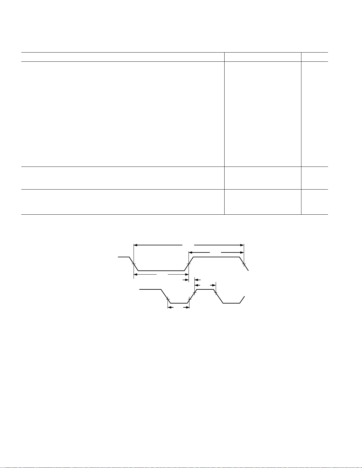
TIMING PARAMETERS
Parameter Min Max Unit
Clock Signals
Signal t
is defined as 0.5 t
CK
frequency equal to half the instruction rate; a 10 MHz input clock (which is
equivalent to 100 ns) yields a 50 ns processor cycle (equivalent to 20 MHz). When
values are within the range of 0.5 t
t
CK
all relevant timing parameters to obtain specification value.
Example: t
= 0.5 tCK – 10 ns = 0.5 (50 ns) – 10 ns = 15 ns.
CKH
Timing Requirements:
t
CKIN
t
CKIL
t
CKIH
CLKIN Period 100 150 ns
CLKIN Width Low 20 ns
CLKIN Width High 20 ns
Switching Characteristics:
t
CKL
t
CKH
t
CKOH
CLKOUT Width Low 0.5 tCK – 10 ns
CLKOUT Width High 0.5 tCK – 10 ns
CLKIN High to CLKOUT High 0 20 ns
Control Signals
Timing Requirement:
t
RSP
RESET Width Low 5 t
PWM Shutdown Signals
Timing Requirement:
t
PWMTPW
NOTES
1
Applies after power-up sequence is complete.
Specifications subject to change without notice.
PWMTRIP Width Low t
. The ADMC328 uses an input clock with a
CKIN
period, they should be substituted for
CKIN
CK
CK
1
ns
ns
CLKIN
CLKOUT
t
CKIN
t
CKIL
t
CKL
Figure 1. Clock Signals
t
t
CKOH
CKH
t
CKIH
–4–
REV. B
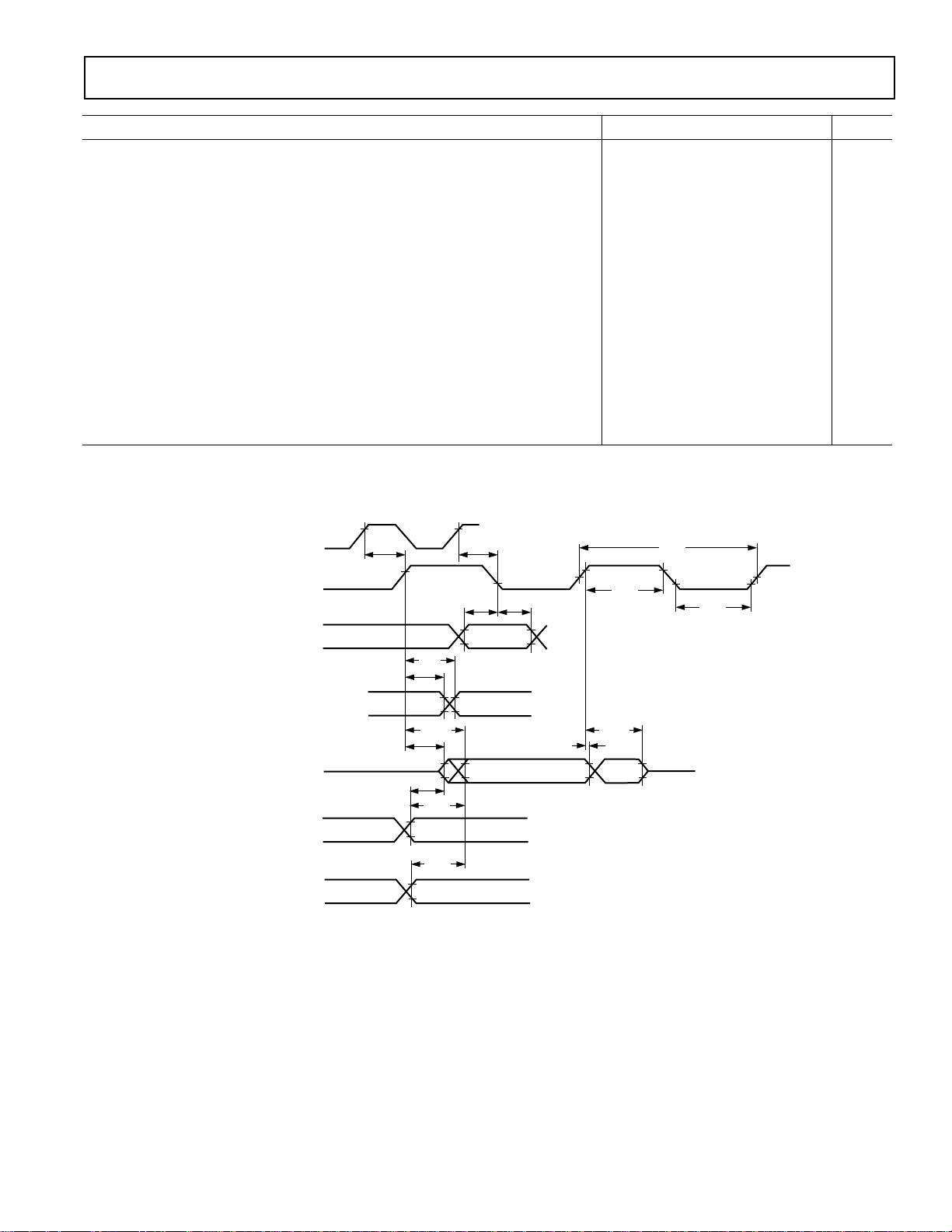
ADMC328
Parameter Min Max Unit
Serial Ports
Timing Requirements:
t
SCK
t
SCS
t
SCH
t
SCP
Switching Characteristics:
t
CC
t
SCDE
t
SCDV
t
RH
t
RD
t
SCDH
t
SCDD
t
TDE
t
TDV
t
RDV
Specifications subject to change without notice.
SCLK Period 100 ns
DR/TFS/RFS Setup before SCLK Low 15 ns
DR/TFS/RFS Hold after SCLK Low 20 ns
SCLKIN Width 40 ns
CLKOUT High to SCLK
OUT
0.25 t
0.25 tCK + 20 ns
CK
SCLK High to DT Enable 0 ns
SCLK High to DT Valid 30 ns
TFS/RFS
TFS/RFS
Hold after SCLK High 0 ns
OUT
Delay from SCLK High 30 ns
OUT
DT Hold after SCLK High 0 ns
SCLK High to DT Disable 30 ns
TFS (Alt) to DT Enable 0 ns
TFS (Alt) to DT Valid 25 ns
RFS (Multichannel, Frame Delay Zero) to DT Valid 30 ns
CLKOUT
SCLK
RFS
TFS
RFS
OUT
TFS
OUT
TFS
(ALTERNATE
FRAME MODE)
(MULTICHANNEL MODE,
FRAME DELAY 0 [MFD = 0])
RFS
DR
DT
t
CC
IN
IN
t
t
SCDE
t
RH
TDE
t
t
RD
SCDV
t
t
RDV
TDV
t
CC
t
t
SCS
SCH
t
t
SCDH
SCDD
t
SCK
t
SCP
t
SCP
Figure 2. Serial Port Timing
REV. B
–5–
ADMC328
WARNING!
ESD SENSITIVE DEVICE
ABSOLUTE MAXIMUM RATINGS*
Supply Voltage (VDD) . . . . . . . . . . . . . . . . . . –0.3 V to +7.0 V
Input Voltage . . . . . . . . . . . . . . . . . . . . . –0.3 V to V
Output Voltage Swing . . . . . . . . . . . . . . –0.3 V to V
+ 0.3 V
DD
+ 0.3 V
DD
Operating Temperature Range (Ambient)
ADMC328Y . . . . . . . . . . . . . . . . . . . . . . –40°C to +105°C
ADMC328T . . . . . . . . . . . . . . . . . . . . . . –40°C to +125°C
Storage Temperature Range . . . . . . . . . . . . –65°C to +150°C
Lead Temperature (5 sec) . . . . . . . . . . . . . . . . . . . . . . . 280°C
*Stresses greater than those listed may cause permanent damage to the device.
These are stress ratings only; functional operation of the device at these or any
other conditions greater than those indicated in the operational sections of this
specification is not implied. Exposure to absolute maximum rating conditions for
extended periods may affect device reliability.
PIN CONFIGURATION
PIO6/CLKOUT
PIO5/RFS1
PIO4/DR1A
PIO3/SCLK1
PIO2/DR1B
PIO1/DT1
PIO0/TFS1
CLKIN
XTAL
V
PWMTRIP
I
SENSE
DD
V2
V1
1
2
3
4
5
6
ADMC328
7
TOP VIEW
(Not to Scale)
8
9
10
11
12
13
14
28
PIO7/AUX1
27
PIO8/AUX0
AL
26
25
AH
BL
24
BH
23
CL
22
CH
21
20
RESET
GND
19
ICONST
18
VAUX2
17
16
VAUX1
15
VAUX0
PIN FUNCTION DESCRIPTIONS
Pin Pin Pin
No. Name Type
1 PIO6/CLKOUT I/O
2 PIO5/RFS1 I/O
3 PIO4/DR1A I/O
4 PIO3/SCLK1 I/O
5 PIO2/DR1B I/O
6 PIO1/DT1 I/O
7 PIO0/TFS1 I/O
8 CLKIN I
9 XTAL O
10 V
DD
SUP
11 PWMTRIP I
12 I
SENSE
I
13 V2 I
14 V1 I
15 VAUX0 I
16 VAUX1 I
17 VAUX2 I
18 ICONST O
19 GND GND
20 RESET I
21 CH O
22 CL O
23 BH O
24 BL O
25 AH O
26 AL O
27 PIO8/AUX0 I/O
28 PIO7/AUX1 I/O
ORDERING GUIDE
Temperature Instruction Package Package
Model Range Rate Description Option
ADMC328YR-xxx-yy –40°C to +105°C 20 MHz 28-Lead Wide Body (SOIC) R-28
ADMC328TR-xxx-yy –40°C to +125°C 20 MHz 28-Lead Wide Body (SOIC) R-28
ADMC328YN-xxx-yy –40°C to +105°C 20 MHz 28-Lead Wide Body (PDIP) N-28
ADMC328TN-xxx-yy –40°C to +125°C 20 MHz 28-Lead Wide Body (PDIP) N-28
NOTES
xxx = customer identification code.
yy = ROM identification code.
To place an order for a custom ROM-coded ADMC328 processor, please request a copy of the ADMC ROM ordering package, available from your Analog Devices
Sales representative.
Analog Devices assesses a charge for each ROM mask generated in addition to a minimum order quantity. Please consult your sales representative for details.
CAUTION
ESD (electrostatic discharge) sensitive device. Electrostatic charges as high as 4000 V readily
accumulate on the human body and test equipment and can discharge without detection.
Although the ADMC328 features proprietary ESD protection circuitry, permanent damage may
occur on devices subjected to high energy electrostatic discharges. Therefore, proper ESD
precautions are recommended to avoid performance degradation or loss of functionality.
–6–
REV. B
ADMC328
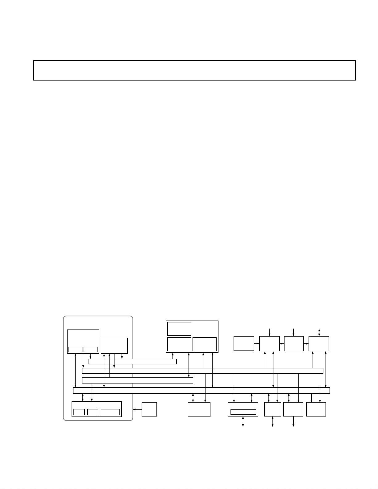
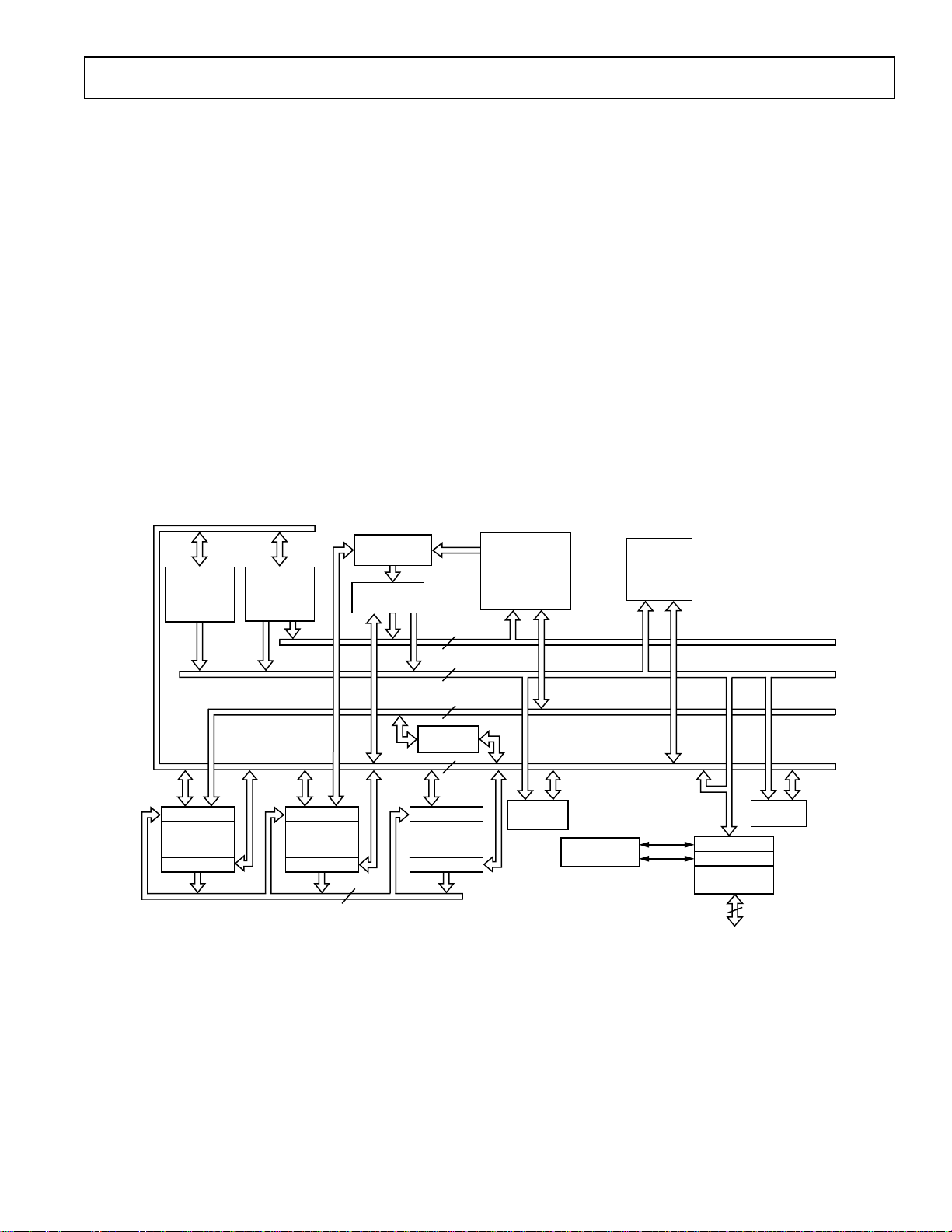
GENERAL DESCRIPTION
The ADMC328 is a low cost, single-chip DSP-based controller,
suitable for permanent magnet synchronous motors and brushless
dc motors. The ADMC328 integrates a 20 MIPS, fixed-point
DSP core with a complete set of motor control and system
peripherals that permits fast, efficient development of motor
controllers.
The DSP core of the ADMC328 is the ADSP-2171, which is
completely code compatible with the ADSP-21xx DSP family
and combines three computational units, data address generators
and a program sequencer. The computational units comprise an
ALU, a multiplier/accumulator (MAC) and a barrel shifter. The
ADSP-2171 adds new instructions for bit manipulation, multipli-
cation (× squared), biased rounding and global interrupt masking.
The system peripherals are the power-on reset circuit (POR),
the watchdog timer and a synchronous serial port. The serial
port is configurable and double buffered, with hardware support
for UART and SCI port emulation.
INSTRUCTION
REGISTER
DATA
ADDRESS
GENERATOR
#1
DATA
ADDRESS
GENERATOR
#2
PROGRAM
SEQUENCER
14
The ADMC328 provides 512 × 24-bit program memory RAM,
4K × 24-bit program memory ROM and 512 × 16-bit data
memory RAM. The program memory ROM contains the userspecified program code and is defined using a single metal layer
mask. The program and data memory RAM can be used for
dynamic data storage.
The motor control peripherals of the ADMC328 comprise a
12-bit analog data acquisition system with five analog input
channels and one dedicated I
function (combining internal
SENSE
amplification, sampling, and overcurrent PWM shutdown
features) and an internal voltage reference. In addition, a threephase, 16-bit, center-based PWM generation unit can be used to
produce high accuracy PWM signals with minimal processor
overhead. The ADMC328 also contains two auxiliary PWM
outputs, and nine lines of digital I/O.
Because the ADMC328 has a limited number of pins, a number
of functions such as the auxiliary PWM and the serial communication port are multiplexed with the nine programmable input/
output (PIO) pins. The pin functions can be independently
selected to allow maximum flexibility for different applications.
PM ROM
4K 3 24
PM RAM
512 3 24
PMA BUS
DM RAM
512 3 16
INPUT REGS
ALU
OUTPUT REGS
INPUT REGS
MAC
OUTPUT REGS
16
14
24
BUS
EXCHANGE
16
INPUT REGS
SHIFTER
OUTPUT REGS
R BUS
CONTROL
LOGIC
Figure 3. DSP Core Block Diagram
DMA BUS
PMD BUS
DMD BUS
COMPANDING
CIRCUITRY
TRANSMIT REG
RECEIVE REG
SERIAL
PORT
6
TIMER
REV. B
–7–

ADMC328
DSP CORE ARCHITECTURE OVERVIEW
Figure 3 is an overall block diagram of the DSP core of the
ADMC328, which is based on the fixed-point ADSP-2171. The
flexible architecture and comprehensive instruction set of the
ADSP-2171 allow the processor to perform multiple operations
in parallel. In one processor cycle (50 ns with a 10 MHz CLKIN)
the DSP core can:
• Generate the next program address.
• Fetch the next instruction.
• Perform one or two data moves.
• Update one or two data address pointers.
• Perform a computational operation.
This all takes place while the processor continues to:
• Receive and transmit through the serial port.
• Decrement the interval timer.
• Generate three-phase PWM waveforms for a power inverter.
• Generate two signals using the 8-bit auxiliary PWM timers.
• Acquire four analog signals.
• Decrement the watchdog timer.
The processor contains three independent computational units:
the arithmetic and logic unit (ALU), the multiplier/accumulator
(MAC) and the shifter. The computational units process 16-bit
data directly and have provisions to support multiprecision computations. The ALU performs a standard set of arithmetic and
logic operations as well as providing support for division primitives. The MAC performs single-cycle multiply, multiply/add,
and multiply/subtract operations with 40 bits of accumulation.
The shifter performs logical and arithmetic shifts, normalization,
denormalization and derive-exponent operations. The shifter
can be used to efficiently implement numeric format control, including floating-point representations.
The internal result (R) bus directly connects the computational
units so that the output of any unit may be the input of any unit
on the next cycle.
A powerful program sequencer and two dedicated data address
generators ensure efficient delivery of operands to these computational units. The sequencer supports conditional jumps and
subroutine calls and returns in a single cycle. With internal loop
counters and loop stacks, the ADMC328 executes looped code
with zero overhead; no explicit jump instructions are required to
maintain the loop.
Two data address generators (DAGs) provide addresses for
simultaneous dual operand fetches from data memory and program memory. Each DAG maintains and updates four address
pointers (I registers). Whenever the pointer is used to access
data (indirect addressing), it is post-modified by the value in
one of four modify (M registers). A length value may be associated with each pointer (L registers) to implement automatic
modulo addressing for circular buffers. The circular buffering
feature is also used by the serial ports for automatic data transfers to and from on-chip memory. DAG1 generates only data
memory address and provides an optional bit-reversal capability.
DAG2 may generate either program or data memory addresses
but has no bit-reversal capability.
Efficient data transfer is achieved with the use of five internal
buses:
• Program memory address (PMA) bus.
• Program memory data (PMD) bus.
• Data memory address (DMA) bus.
• Data memory data (DMD) bus.
• Result (R) bus.
Program memory can store both instructions and data, permitting the ADMC328 to fetch two operands in a single cycle—
one from program memory and one from data memory. The
ADMC328 can fetch an operand from on-chip program memory
and the next instruction in the same cycle.
The ADMC328 writes data from its 16-bit registers to the 24-bit
program memory using the PX register to provide the lower
eight bits. When it reads data (not instructions) from 24-bit program memory to a 16-bit data register, the lower eight bits are
placed in the PX register.
The ADMC328 can respond to a number of distinct DSP core
and peripheral interrupts. The DSP interrupts comprise a serial
port receive interrupt, a serial port transmit interrupt, a timer
interrupt, and two software interrupts. Additionally, the motor
control peripherals include two PWM interrupts and a PIO interrupt.
The serial port (SPORT1) provides a complete synchronous
serial interface with optional companding in hardware and a
wide variety of framed and unframed data transmit and receive
modes of operation. SPORT1 can generate an internal programmable serial clock or accept an external serial clock.
A programmable interval counter is also included in the DSP
core and can be used to generate periodic interrupts. A 16-bit
count register (TCOUNT) is decremented every n processor
cycles, where n–1 is a scaling value stored in the 8-bit TSCALE
register. When the value of the counter reaches zero, an interrupt
is generated, and the count register is reloaded from a 16-bit
period register (TPERIOD).
The ADMC328 instruction set provides flexible data moves
and multifunction (one or two data moves with a computation)
instructions. Each instruction is executed in a single 50 ns processor cycle (for a 10 MHz CLKIN). The ADMC328 assembly
language uses an algebraic syntax for ease of coding and readability. A comprehensive set of development tools supports
program development. For further information on the DSP
core, refer to the ADSP-2100 Family User’s Manual, Third Edition,
with particular reference to the ADSP-2171.
–8–
REV. B

ADMC328
Serial Port
The ADMC328 incorporates a complete synchronous serial
port (SPORT1) for serial communication and multiprocessor
communication. The following is a brief list of capabilities of the
ADMC328 SPORT1. Refer to the ADSP-2100 Family User’s
Manual, Third Edition, for further details.
• SPORT1 is bidirectional and has a separate, double-buffered
transmit and receive section.
• SPORT1 can use an external serial clock or generate its own
serial clock internally.
• SPORT1 has independent framing for the receive and transmit sections. Sections run in a frameless mode or with frame
synchronization signals internally or externally generated.
Frame synchronization signals are active high or inverted,
with either of two pulsewidths and timings.
• SPORT1 supports serial data word lengths from 3 bits to 16
bits and provides optional A-law and µ-law companding ac-
cording to ITU (formerly CCITT) recommendation G.711.
• SPORT1 receive and transmit sections can generate unique
interrupts on completing a data word transfer.
• SPORT1 can receive and transmit an entire circular buffer of
data with only one overhead cycle per data word. An interrupt
is generated after a data buffer transfer.
• SPORT1 can be configured to have two external interrupts
(IRQ0 and IRQ1), and the Flag In and Flag Out signals.
The internally generated serial clock may still be used in this
configuration.
• SPORT1 has two data receive pins (DR1A and DR1B), which
are internally multiplexed onto the one DR1 port of the
SPORT1. The particular data receive pin selected is determined by a bit in the MODECTRL register.
PIN FUNCTION DESCRIPTION
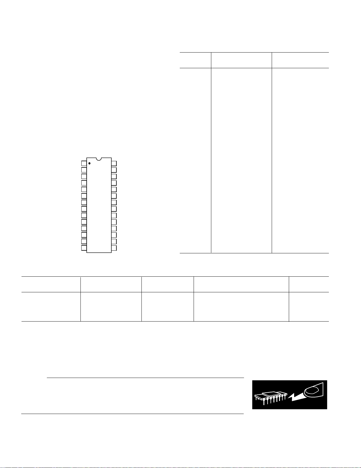
The ADMC328 is available in a 28-lead SOIC package and a
28-lead PDIP package. Table I describes the pins.
Table I. Pin List
Group # of Input/
Name Pins Output Function
RESET 1 I Processor Reset Input
SPORT1
CLKOUT
CLKIN, XTAL 2 I, O External Clock or Quartz
PIO0–PIO8
AUX0–AUX1
AH–CL 6 O PWM Outputs
PWMTRIP 1 I PWM Trip Signal
V1–V2 2 I Analog Inputs
VAUX0–VAUX2 3 I Auxiliary Analog Input
I
SENSE
ICONST 1 O ADC Constant Current Source
V
GND 1 Ground
NOTE
1
Multiplexed pins, selectable individually through the PIOSEL ECT and
PIODATA1 registers.
REV. B
DD
1
1
6 I/O Serial Port 1 Pins (TFS1,
RFS1, DT1, DR1A, DR1B,
SCLK1)
1 O Processor Clock Output
1
9 I/O Digital I/O Port Pins
1
2 O Auxiliary PWM Outputs
1 I Current Sense Amplifier Input
1 Power Supply
Crystal Connection Point
–9–
INTERRUPT OVERVIEW
The ADMC328 can respond to 16 different interrupt sources
with minimal overhead, five of which are internal DSP core
interrupts and 11 are from the motor control peripherals. The five
DSP core interrupts are SPORT1 receive (or IRQ0) and transmit (or IRQ1), the internal timer, and two software interrupts.
The motor control peripheral interrupts are the nine programmable I/Os and two from the PWM (PWMSYNC pulse and
PWMTRIP). All motor control interrupts are multiplexed into the
DSP core through the peripheral IRQ2 interrupt. The interrupts
are internally prioritized and individually maskable. A detailed
description of the entire interrupt system of the ADMC328 is
presented later, following a more detailed description of each
peripheral block.
Memory Map
The ADMC328 has two distinct memory types: program memory
and data memory. In general, program memory contains user
code and coefficients, while the data memory is used to store
variables and data during program execution. Both program
memory RAM and ROM are provided on the ADMC328. Pro-
gram memory RAM is arranged as one contiguous 512 × 24-bit
block, starting at address 0x0000. Program memory ROM is a
4K × 24-bit block located at address 0x0800. Data memory is
arranged as a 512 × 16-bit block starting at address 0x3800. The
motor control peripherals are memory mapped into a region of
the data memory space starting at 0x2000. The complete program
and data memory maps are given in Tables II and III, respectively.
Table II. Program Memory Map
Memory
Address Range Type Function
0x0000–0x002F RAM Interrupt Vector Table
0x0030–0x01FF RAM User Program Memory
0x0200–0x07FF Reserved
0x0800–0x17FF ROM User Program Memory
0x1800–0x3FFF Reserved
Table III. Data Memory Map
Memory
Address Range Type Function
0x0000–0x1FFF Reserved
0x2000–0x20FF Memory Mapped Registers
0x2100–0x37FF Reserved
0x3800–0x39FF RAM User Data Memory
0x3A00–0x3BFF RAM Reserved
0x3C00–0x3FFF Memory Mapped Registers
ADMC328
SYSTEM INTERFACE
Figure 4 shows a basic system configuration for the ADMC328
with an external crystal.
CLKOUT
ADMC328
RESET
XTAL
CLKIN
22pF
10MHz
22pF
Figure 4. Basic System Configuration
Clock Signals
The ADMC328 can be clocked either by a crystal or a TTLcompatible clock signal. For normal operation, the CLKIN
input cannot be halted, changed during operation, or operated
below the specified minimum frequency. If an external clock is
used, it should be a TTL-compatible signal running at half the
instruction rate. The signal is connected to the CLKIN pin of
the ADMC328. In this mode, with an external clock signal, the
XTAL pin must be left unconnected. The ADMC328 uses an
input clock with a frequency equal to half the instruction rate;
a 10 MHz input clock yields a 50 ns processor cycle (which is
equivalent to 20 MHz). Normally, instructions are executed in a
single processor cycle. All device timing is relative to the internal
instruction rate, which is indicated by the CLKOUT signal
when enabled.
Because the ADMC328 includes an on-chip oscillator feedback
circuit, an external crystal may be used instead of a clock source, as
shown in Figure 4. The crystal should be connected across the
CLKIN and XTAL pins, with two capacitors as shown in Figure 4.
A parallel-resonant, fundamental frequency, microprocessor-grade
crystal should be used. A clock output signal (CLKOUT) is
generated by the processor at the processor’s cycle rate of twice
the input frequency.
Reset
The ADMC328 DSP core and peripherals must be correctly reset when the device is powered up to assure proper initialization.
The ADMC328 contains an integrated power-on reset (POR)
circuit that provides a complete system reset on power-up and
power-down. The POR circuit monitors the voltage on the
ADMC328 V
reset while V
When this voltage is exceeded, the ADMC328 is held in reset
for an additional 2
power-down, when the voltage on the V
V
RST–VHYST
pin and holds the DSP core and peripherals in
DD
is less than the threshold voltage level, V
DD
16
DSP clock cycles (t
in Figure 5). On
RST
pin falls below
DD
RST
.
, the ADMC328 will be reset. Also, if the external
RESET pin is actively pulled low at any time after power-up, a
complete hardware reset of the ADMC328 is initiated.
V
RST
V
RESET
DD
t
RST
V
RST – VHYST
Figure 5. Power-On Reset Operation
The ADMC328 reset sets all internal stack pointers to the empty
stack condition, masks all interrupts, clears the MSTAT register
and performs a full reset of all of the motor control peripherals.
Following a power-up, it is possible to initiate a DSP core and
motor control peripheral reset by pulling the RESET pin low.
The RESET signal must meet the minimum pulsewidth specification, t
. Following the reset sequence, the DSP core starts
RSP
executing code from the internal PM ROM located at 0x0800.
DSP Control Registers
The DSP core has a system control register, SYSCNTL, memory
mapped at DM (0x3FFF). SPORT1 is configured as a serial
port when Bit 10 is set, or as flags and interrupt lines when this
bit is cleared. For proper operation of the ADMC328, all other
bits in this register must be cleared.
The DSP core has a wait state control register, MEMWAIT,
memory mapped at DM (0x3FFE). The default value of this
register is 0xFFFF. For proper operation of the ADMC328 this
register must be set to 0x8000.
The configuration of both the SYSCNTL and MEMWAIT
registers of the ADMC328 are shown at the end of this data sheet.
THREE-PHASE PWM CONTROLLER
Overview
The PWM generator block of the ADMC328 is a flexible, programmable, three-phase PWM waveform generator that can be
programmed to generate the required switching patterns to drive
a three-phase voltage source inverter for ac induction motors
(ACIM) or permanent magnet synchronous motors (PMSM).
In addition, the PWM block contains special functions that considerably simplify the generation of the required PWM switching
patterns for control of electronically commutated motors (ECM)
or brushless dc motors (BDCM).
The PWM generator produces three pairs of active high PWM
signals on the six PWM output pins (AH, AL, BH, BL, CH,
and CL). The six PWM output signals consist of three high side
drive signals (AH, BH, and CH) and three low side drive signals
(AL, BL, and CL). The switching frequency, dead time and
minimum pulsewidths of the generated PWM patterns are programmable using respectively the PWMTM, PWMDT, and
PWMPD registers. In addition, three registers (PWMCHA,
PWMCHB, and PWMCHC) control the duty cycles of the three
pairs of PWM signals.
Each of the six PWM output signals can be enabled or disabled
by separate output enable bits of the PWMSEG register. In
addition, three control bits of the PWMSEG register permit
crossover of the two signals of a PWM pair for easy control of
ECM or BDCM. In crossover mode, the PWM signal destined
for the high side switch is diverted to the complementary low
side output, and the signal destined for the low side switch is
diverted to the corresponding high side output signal.
In many applications, there is a need to provide an isolation
barrier in the gate-drive circuits that turn on the power devices
of the inverter. In general, there are two common isolation techniques: optical isolation using optocouplers, and transformer
isolation using pulse transformers. The PWM controller of the
ADMC328 permits mixing of the output PWM signals with a
high frequency chopping signal to permit an easy interface to
such pulse transformers. The features of this gate-drive chopping mode can be controlled by the PWMGATE register. There
is an 8-bit value within the PWMGATE register that directly
–10–
REV. B
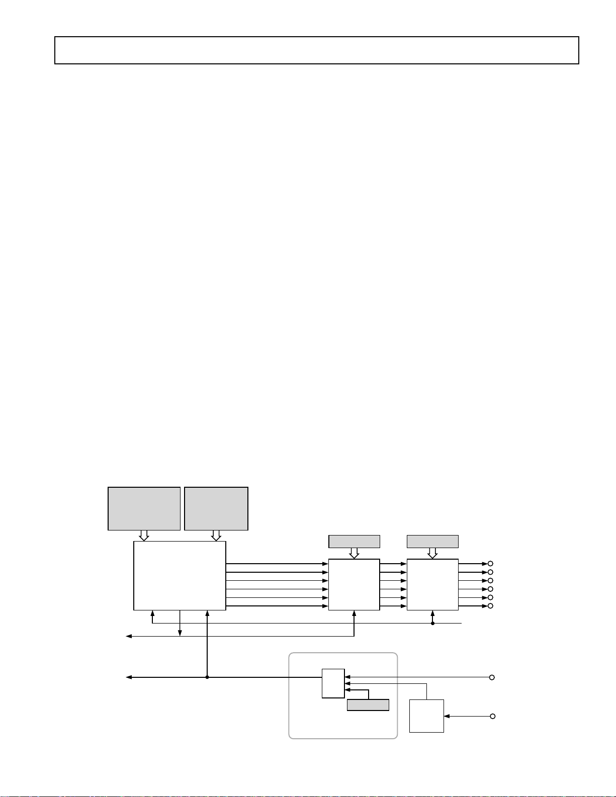
ADMC328
controls the chopping frequency. In addition, high frequency
chopping can be independently enabled for the high side and the
low side outputs using separate control bits in the PWMGATE
register.
The PWM generator is capable of operating in two distinct
modes: single update mode or double update mode. In single
update mode, the duty cycle values are programmable only once
per PWM period, so that the resultant PWM patterns are symmetrical about the midpoint of the PWM period. In the double
update mode, a second updating of the PWM duty cycle values
is implemented at the midpoint of the PWM period. In this mode,
it is possible to produce asymmetrical PWM patterns that produce lower harmonic distortion in three-phase PWM inverters.
This technique also permits the closed-loop controller to change
the average voltage applied to the machine winding at a faster
rate, allowing wider closed-loop bandwidths to be achieved. The
operating mode of the PWM block (single or double update mode)
is selected by a control bit in MODECTRL register.
The PWM generator of the ADMC328 also provides an internal
signal that synchronizes the PWM switching frequency to the
A/D operation. In single update mode, a PWMSYNC pulse is
produced at the start of each PWM period. In double update
mode, an additional PWMSYNC pulse is produced at the midpoint of each PWM period. The width of the PWMSYNC pulse
is programmable through the PWMSYNCWT register.
The PWM signals produced by the ADMC328 can be shut off
in a number of different ways. First, there is a dedicated asynchronous PWM shutdown pin, PWMTRIP, which, when brought
LO, instantaneously places all six PWM outputs in the OFF
state. In addition, PWM shutdown is initiated when the voltage
on the analog input pin (I
) is pulled below the trip volt-
SENSE
age level, corresponding to an overcurrent fault. Because these
two hardware shutdown mechanisms are asynchronous, and
the associated PWM disable circuitry does not use clocked logic,
the PWM will shut down even if the DSP clock is not running.
The PWM system may also be shut down from software by writing to the PWMSWT register.
Status information about the PWM system of the ADMC328 is
available to the user in the SYSSTAT register. In particular, the
state of PWMTRIP is available, as well as a status bit that indicates whether operation is in the first half or the second half of
the PWM period.
A functional block diagram of the PWM controller is shown in
Figure 6. The generation of the six output PWM signals on pins
AH to CL is controlled by four important blocks:
• The three-phase PWM timing unit, which is the core of the
PWM controller, generates three pairs of complemented and
dead-time-adjusted center-based PWM signals.
• The output control unit allows the redirection of the outputs
of the three-phase timing unit for each channel to either the
high side or the low side output. In addition, the output control unit allows individual enabling/disabling of each of the six
PWM output signals.
• The GATE drive unit provides the high chopping frequency
and its subsequent mixing with the PWM signals.
• The PWM shutdown controller manages the three PWM
shutdown modes (via the PWMTRIP pin, the analog block or
the PWMSWT register) and generates the correct RESET signal
for the Timing Unit.
• The PWM controller is driven by a clock at the same frequency
as the DSP instruction rate, CLKOUT, and is capable of
generating two interrupts to the DSP core. One interrupt is
generated on the occurrence of a PWMSYNC pulse, and the
other is generated on the occurrence of any PWM shutdown
action.
PWM CONFIGURATION
REGISTERS
PWMTM (15...0)
PWMDT (9...0)
PWMPD (15...0)
PWMSYNCWT (7...0)
MODECTRL (6)
THREE-PHASE
PWM TIMING
CLK RESET
PWMSYNC
TO INTERRUPT
CONTROLLER
PWMTRIP
PWM DUTY CYCLE
REGISTERS
PWMCHA (15...0)
PWMCHB (15...0)
PWMCHC (15...0)
PWMSEG (8...0)
OR
OUTPUT
CONTROL
UNIT
SYNC
PWMSWT (0)
UNIT
SYNC
PWM SHUTDOWN CONTROLLER
Figure 6. Overview of the PWM Controller of the ADMC328
PWMGATE (9...0)
GATE
DRIVE
UNIT
CLK
OVER
CURRENT
TRIP
ANALOG BLOCK
CLKOUT
AH
AL
BH
BL
CH
CL
PWMTRIP
I
SENSE
REV. B
–11–

ADMC328
Three-Phase Timing Unit
The 16-bit three-phase timing unit is the core of the PWM controller and produces three pairs of pulsewidth modulated signals
with high resolution and minimal processor overhead. There are
four main configuration registers (PWMTM, PWMDT, PWMPD
and PWMSYNCWT) that determine the fundamental characteristics of the PWM outputs. In addition, the operating mode
of the PWM (single or double update mode) is selected by Bit 6
of the MODECTRL register. These registers, in conjunction with
the three 16-bit duty cycle registers (PWMCHA, PWMCHB and
PWMCHC), control the output of the three-phase timing unit.
PWM Switching Frequency: PWMTM Register
The PWM switching frequency is controlled by the PWM
period register, PWMTM. The fundamental timing unit of
the PWM controller is t
CK
= 1/f
CLKOUT
where f
CLKOUT
is the
CLKOUT frequency (DSP instruction rate). Therefore, for a
20 MHz CLKOUT, the fundamental time increment is 50 ns.
The value written to the PWMTM register is effectively the
number of t
clock increments in half a PWM period. The
CK
required PWMTM value is a function of the desired PWM
switching frequency (f
PWMTM
) and is given by:
PWM
f
CLKOUT
=
f
×
2
PWM
f
CLKIN
=
f
PWM
Therefore, the PWM switching period, TS, can be written as:
T PWMTM t
=× ×2
SCK
For example, for a 20 MHz CLKOUT and a desired PWM
switching frequency of 10 kHz (T
= 100 µs), the correct value
S
to load into the PWMTM register is:
PWMTM x E=
20 10
××
21010
3
=
1000 0 3 8
6
×
The largest value that can be written to the 16-bit PWMTM
register is 0xFFFF = 65,535, which corresponds to a minimum
PWM switching frequency of:
fHz
PWM,min
20 10
=
×
2 65 535
=
,
153
6
×
for a CLKOUT frequency of 20 MHz.
PWM Switching Dead Time: PWMDT Register
The second important PWM block parameter that must be
initialized is the switching dead time. This is a short delay time
introduced between turning off one PWM signal (for example
AH) and turning on its complementary signal, AL. This short
time delay is introduced to permit the power switch being turned
off to completely recover its blocking capability before the
complementary switch is turned on. This time delay prevents a
potentially destructive short-circuit condition from developing
across the dc link capacitor of a typical voltage source inverter.
Dead time is controlled by the PWMDT register. The dead
time is inserted into the three pairs of PWM output signals. The
dead time, T
, is related to the value in the PWMDT register by:
D
T PWMDT t
=××=×22
DCK
PWMDT
f
CLKOUT
Therefore, a PWMDT value of 0x00A (= 10), introduces a 1 µs
delay between the turn-off of any PWM signal (for example AH)
and the turn-on of its complementary signal (AL). The amount
of the dead time can therefore be programmed in increments of
–12–
2 t
(or 100 ns for a 20 MHz CLKOUT). The PWMDT register
CK
is a 10-bit register. For a CLKOUT rate of 20 MHz its maximum
value of 0x3FF (= 1023) corresponds to a maximum programmed
dead time of:
T
= 1023 × 2 × t
Dmax
= 1023 × 2 × 50 × 10
CK
–9
sec
= 102 µs
The dead time can be programmed to zero by writing 0 to the
PWMDT register.
PWM Operating Mode: MODECTRL and SYSSTAT Registers
The PWM controller of the ADMCF328 can operate in two distinct modes: single update mode and double update mode. The
operating mode of the PWM controller is determined by the
state of Bit 6 of the MODECTRL register. If this bit is cleared, the
PWM operates in the single update mode. Setting Bit 6 places
the PWM in the double update mode. By default, following
either a peripheral reset or power-on, Bit 6 of the MODECTRL
register is cleared. This means that the default operating mode
is single update mode.
In single update mode, a single PWMSYNC pulse is produced
in each PWM period. The rising edge of this signal marks
the start of a new PWM cycle and is used to latch new values
from the PWM configuration registers (PWMTM, PWMDT,
PWMPD and PWMSYNCWT) and the PWM duty cycle
registers (PWMCHA, PWMCHB and PWMCHC) into the
three-phase timing unit. The PWMSEG register is also latched
into the output control unit on the rising edge of the PWMSYNC
pulse. In effect, this means that the parameters of the PWM
signals can be updated only once per PWM period at the start of
each cycle. Thus, the generated PWM patterns are symmetrical
about the midpoint of the switching period.
In double update mode, there is an additional PWMSYNC pulse
produced at the midpoint of each PWM period. The rising edge
of this new PWMSYNC pulse is again used to latch new values
of the PWM configuration registers, duty cycle registers and the
PWMSEG register. As a result, it is possible to alter both the
characteristics (switching frequency, dead time, minimum pulsewidth and PWMSYNC pulsewidth) and the output duty cycles
at the midpoint of each PWM cycle. Consequently, it is possible to produce PWM switching patterns that are no longer
symmetrical about the midpoint of the period (asymmetrical
PWM patterns).
In the double update mode, operation in the first half or the
second half of the PWM cycle is indicated by Bit 3 of the
SYSSTAT register. In double update mode, this bit is cleared
during operation in the first half of each PWM period (between
the rising edge of the original PWMSYNC pulse and the rising
edge of the new PWMSYNC pulse, which is introduced in
double update mode). Bit 3 of the SYSSTAT register is set
during the second half of each PWM period. If required, a user
may determine the status of this bit during a PWMSYNC interrupt service routine.
The advantages of the double update mode are that lower harmonic voltages can be produced by the PWM process and wider
control bandwidths are possible. However, for a given PWM
switching frequency, the PWMSYNC pulses occur at twice the
rate in the double update mode. Because new duty cycle values
must be computed in each PWMSYNC interrupt service routine,
there is a larger computational burden on the DSP in the double
update mode.
REV. B

ADMC328
Width of the PWMSYNC Pulse: PWMSYNCWT Register
The PWM controller of the ADMCF328 produces an internal
PWM synchronization pulse at a rate equal to the PWM switching
frequency in single update mode and at twice the PWM frequency
in the double update mode. This PWMSYNC synchronizes
the operation of the PWM unit with the A/D converter system.
The width of this PWMSYNC pulse is programmable by the
PWMSYNCWT register. The width of the PWMSYNC pulse,
T
PWMSYNC
which means that the width of the pulse is programmable from t
to 256 t
, is given by:
T t PWMSYNCWT
PWMSYNC CK
(corresponding to 50 ns to 12.8 µs for a CLKOUT rate
CK
=× +
()
1
CK
of 20 MHz). Following a reset, the PWMSYNCWT register con-
tains 0x27 (= 39) so that the default PWMSYNC width is 2.0 µs.
PWM Duty Cycles: PWMCHA, PWMCHB, PWMCHC
Registers
The duty cycles of the six PWM output signals are controlled
by the three duty cycle registers, PWMCHA, PWMCHB, and
PWMCHC. The integer value in the register PWMCHA controls
the duty cycle of the signals on AH and AL. PWMCHB controls
the duty cycle of the signals on BH and BL, and PWMCHC
controls the duty cycle of the signals on CH and CL. The duty
cycle registers are programmed in integer counts of the fundamental time unit, t
, and define the desired on-time of the
CK
high-side PWM signal produced by the three-phase timing unit
over half the PWM period. The switching signals produced by
the three-phase timing unit are also adjusted to incorporate the
programmed dead time value in the PWMDT register.
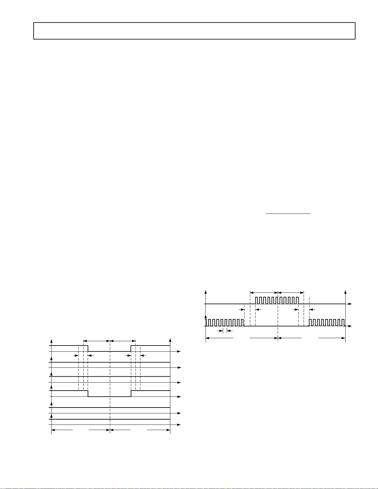
The PWM is center-based. This means that in single update mode
the resulting output waveforms are symmetrical and centered in
the PWMSYNC period. Figure 7 presents a typical PWM timing diagram illustrating the PWM-related registers’ (PWMCHA,
PWMTM, PWMDT, and PWMSYNCWT) control over the
waveform timing in both half cycles of the PWM period. The
magnitude of each parameter in the timing diagram is determined
by multiplying the integer value in each register by t
(typically
CK
50 ns). It may be seen in the timing diagram how dead time is
incorporated into the waveforms by moving the switching edges
away from the instants set by the PWMCHA register.
PWMCHA
AH
2 3 PWMDT
AL
PWMSYNC
SYSSTAT (3)
PWMTM
PWMCHA
2 3 PWMDT
PWMSYNCWT + 1
PWMTM
Figure 7. Typical PWM Outputs of Three-Phase Timing
Unit in Single Update Mode
Each switching edge is moved by an equal amount (PWMDT
× t
) to preserve the symmetrical output patterns. The PWMSYNC
CK
pulse, whose width is set by the PWMSYNCWT register, is also
shown. Bit 3 of the SYSSTAT register indicates which half cycle
is active. This can be useful in double update mode, as will be
discussed later.
The resultant on-times of the PWM signals shown in Figure 7
may be written as:
T PWMCHA PWMDT t
=× ×
22( –)
AH CK
T PWMTM PWMCHA PWMDT t
=× ×
AL CK
(– –)
The corresponding duty cycles are:
d
==
AH
d
==
AL
T
T
PWMCHA PWMDT
AH
T
S
PWMTM PWMCHA PWMDT
AL
T
S
–
PWMTM
––
PWMTM
Obviously, negative values of TAH and TAL are not permitted
because the minimum permissible value is zero, corresponding
to a 0% duty cycle. In a similar fashion, the maximum value is
, corresponding to a 100% duty cycle.
T
S
The output signals from the timing unit for operation in double
update mode are shown in Figure 8. This illustrates a completely
general case where the switching frequency, dead time and duty
cycle are all changed in the second half of the PWM period. Of
course, the same value for any or all of these quantities could be
used in both halves of the PWM cycle. However, it can be seen
that there is no guarantee that symmetrical PWM signals will be
produced by the timing unit in this double update mode. Additionally, it is seen that the dead time is inserted into the PWM
signals in the same way as in the single update mode.
AH
AL
PWMSYNC
SYSSTAT (3)
2 3 PWMDT
PWMSYNCWT1 + 1
PWMTM
PWMCHA
1
1
1
PWMCHA
2
2 3 PWMDT
PWMSYNCWT2 + 1
PWMTM
2
2
Figure 8. Typical PWM Outputs of Three-Phase Timing
Unit in Double Update Mode
In general, the on-times of the PWM signals in double update
mode are defined by:
T
– PWMDT
TAL = (PWMTM1 + PWMTM2 – PWMCHA
– PWMCHA2 – PWMDT1 – PWMDT
= (PWMCHA1 + PWMCHA2 – PWMDT
AH
) × t
2
CK
1
2
1
) × t
CK
where the subscript 1 refers to the value of that register during
the first half cycle and the subscript 2 refers to the value during
the second half cycle. The corresponding duty cycles are:
REV. B
–13–

ADMC328
T
d
d
AH
=
AH
T
S
PWMCHA PWMCHA
()
=
PWMTM PWMTM
()
PWMDT PWMDT
()
–
PWMTM PWMTM
()
T
AL
=
AL
T
S
PWMTM PWMTM PWMCHA
()
=
PWCHA PWMDT PWMDT
()
−
()
+
12
+
12
+
12
+
12
++
12 1
PWMTM PWMTM
()
++
212
PWMTM PWMTM
+
12
+
12
because for the completely general case in double update mode,
the switching period is given by:
T
= (PWMTM1 + PWMTM
S
) × t
2
CK
Again, the values of TAH and TAL are constrained to lie between
zero and T
.
S
PWM signals similar to those illustrated in Figure 7 and Figure
8 can be produced on the BH, BL, CH, and CL outputs by programming the PWMCHB and PWMCHC registers in a manner
identical to that described for PWMCHA.
The PWM controller does not produce any PWM outputs until
all of the PWMTM, PWMCHA, PWMCHB, and PWMCHC
registers have been written to at least once. After these registers
have been written, the counters in the three-phase timing unit
are enabled. Writing to these registers also starts the main PWM
timer. If during initialization, the PWMTM register is written
after the PWMCHA, PWMCHB, and PWMCHC registers,
then the first PWMSYNC pulse (and interrupt if enabled) will
be generated (1.5 × t
× PWMTM) seconds after the initial
CK
write to the PWMTM register in single update mode. In double
update mode, the first PWMSYNC pulse will be generated
× PWMTM) seconds after the initial write to the PWMTM
(t
CK
register in single update mode.
Effective PWM Resolution
In single update mode, the same values of PWMCHA, PWMCHB
and PWMCHC are used to define the on-times in both half
cycles of the PWM period. As a result, the effective resolution of
the PWM generation process is 2 t
(or 100 ns for a 20 MHz
CK
CLKOUT) since incrementing one of the duty cycle registers by
one changes the resultant on-time of the associated PWM signals by t
in each half period (or 2 tCK for the full period).
CK
In double update mode, improved resolution is possible since
different values of the duty cycles registers are used to define the
on-times in both the first and second halves of the PWM period.
As a result, it is possible to adjust the on-time over the whole
period in increments of t
PWM resolution of t
. This corresponds to an effective
CK
in double update mode (or 50 ns for a
CK
20 MHz CLKOUT).
The achievable PWM switching frequency at a given PWM
resolution is tabulated in Table IV.
Table IV. Achievable PWM Resolution in Single and Double
Update Modes
Resolution Single Update Mode Double Update Mode
(Bit) PWM Frequency (kHz) PWM Frequency (kHz)
8 39.1 78.1
9 19.5 39.1
10 9.8 19.5
11 4.9 9.8
12 2.4 4.9
Minimum Pulsewidth: PWMPD Register
In many power converter switching applications, it is desirable
to eliminate PWM switching pulses shorter than a certain width.
It takes a finite time to both turn on and turn off modern power
semiconductor devices. Therefore, if the width of any of the PWM
pulses is shorter than some minimum value, it may be desirable to
completely eliminate the PWM switching for that particular cycle.
The allowable minimum on-time for any of the six PWM outputs for half a PWM period that can be produced by the PWM
controller may be programmed using the PWMPD register. The
minimum on-time is programmed in increments of t
so that
CK
the minimum on-time that will be produced for any half PWM
period, T
, is related to the value in the PWMPD register by:
MIN
T
= PWMPD × t
MIN
CK
A PWMPD value of 0x002 defines a permissible minimum
on-time of 100 ns for a 20 MHz CLKOUT.
In each half cycle of the PWM, the timing unit checks the ontime of each of the six PWM signals. If any of the times is found
to be less than the value specified by the PWMPD register, the
corresponding PWM signal is turned OFF for the entire half
period, and its complementary signal is turned completely ON.
Consider the example where PWMTM = 200, PWMCHA = 5,
PWMDT = 3, and PWMPD = 10 with a CLKOUT of 20 MHz
while operating in single update mode. For this case, the PWM
switching frequency is 50 kHz and the dead time is 300 ns. The
minimum permissible on-time of any PWM signal over one-half
of any period is 500 ns. Clearly, for this example, the dead-time
adjusted on-time of the AH signal for one-half a PWM period is
(5–3) × 50 ns = 100 ns. Because this is less than the minimum
permissible value, output AH of the timing unit will remain
OFF (0% duty cycle). Additionally, the AL signal will be turned
ON for the entire half period (100% duty cycle).
Output Control Unit: PWMSEG Register
The operation of the output control unit is managed by the 9-bit
read/write PWMSEG register. This register sets two distinct
features of the output control unit that are directly useful in the
control of ECM or BDCM.
The PWMSEG register contains three crossover bits, one for each
pair of PWM outputs. Setting Bit 8 of the PWMSEG register
enables the crossover mode for the AH/AL pair of PWM signals;
setting Bit 7 enables crossover on the BH/BL pair of PWM signals;
and setting Bit 6 enables crossover on the CH/CL pair of PWM
signals. If crossover mode is enabled for any pair of PWM signals,
the high-side PWM signal from the timing unit (for example
AH) is diverted to the associated low-side output of the output
control unit so that the signal will ultimately appear at the AL
pin. Of course, the corresponding low-side output of the timing
unit is also diverted to the complementary high-side output of
–14–
REV. B
ADMC328
PWMTM
PWMTM
[4 3 (GDCLK+1) 3
t
CK
]
2 3 PWMDT
2 3 PWMDT
PWMCHA
PWMCHA
the output control unit so that the signal appears at Pin AH.
Following a reset, the three crossover bits are cleared so that the
crossover mode is disabled on all three pairs of PWM signals.
The PWMSEG register also contains six bits (Bits 0 to 5) that
can be used to individually enable or disable each of the six PWM
outputs. If the associated bit of the PWMSEG register is set,
the corresponding PWM output is disabled regardless of the
value of the corresponding duty cycle register. This PWM output
signal will remain in the OFF state as long as the corresponding
enable/disable bit of the PWMSEG register is set. The PWM
output enable function gates the crossover function. After a
reset, all six enable bits of the PWMSEG register are cleared,
thereby enabling all PWM outputs by default.
In a manner identical to the duty cycle registers, the PWMSEG is
latched on the rising edge of the PWMSYNC signal so that changes
to this register only become effective at the start of each PWM
cycle in single update mode. In double update mode, the PWMSEG register can also be updated at the midpoint of the PWM cycle.
In the control of an ECM, only two inverter legs are switched
at any time, and often the high-side device in one leg must be
switched ON at the same time as the low-side driver in a second
leg. Therefore, by programming identical duty cycles for two PWM
channels (for example, let PWMCHA = PWMCHB) and setting
Bit 7 of the PWMSEG register to crossover the BH/BL pair of
PWM signals, it is possible to turn ON the high-side switch of
Phase A and the low-side switch of Phase B at the same time. In
the control of an ECM, one inverter leg (Phase C in this example)
is disabled for a number of PWM cycles. This disable may be
implemented by disabling both the CH and CL PWM outputs
by setting Bits 0 and 1 of the PWMSEG register. This is illustrated in Figure 9 where it can be seen that both the AH and
BL signals are identical, because PWMCHA = PWMCHB, and
the crossover bit for Phase B is set. In addition, the other four
signals (AL, BH, CH, and CL) have been disabled by setting
the appropriate enable/disable bits of the PWMSEG register.
For the situation illustrated in Figure 9, the appropriate value
for the PWMSEG register is 0x00A7. In ECM operation, because each inverter leg is disabled for certain periods of time,
the PWMSEG register is changed based upon the position of
the rotor shaft (motor commutation).
Gate Drive Unit: PWMGATE Register
The gate drive unit of the PWM controller adds features that
simplify the design of isolated gate drive circuits for PWM
inverters. If a transformer-coupled power device gate drive
amplifier is used, the active PWM signal must be chopped at
a high frequency. The PWMGATE register allows the programming of this high frequency chopping mode. The chopped active
PWM signals may be required for the high-side drivers only, for
the low-side drivers only, or for both the high-side and low-side
switches. Therefore, independent control of this mode for both
high- and low-side switches is included with two separate control bits in the PWMGATE register.
Typical PWM output signals with high-frequency chopping
enabled on both high-side and low-side signals are shown in
Figure 10. Chopping of the high-side PWM outputs (AH, BH,
and CH) is enabled by setting Bit 8 of the PWMGATE register.
Chopping of the low-side PWM outputs (AL, BL, and CL) is
enabled by setting Bit 9 of the PWMGATE register. The high
chopping frequency is controlled by the 8-bit word (GDCLK)
written to Bits 0 to 7 of the PWMGATE register. The period
and the frequency of this high frequency carrier are:
T GDCLK t
=× +
41
CHOP CK
f
CHOP
()
[]
f
=
CLKOUT
GDCLK
×+
41
()
[]
×
The GDCLK value may range from 0 to 255, corresponding
to a programmable chopping frequency rate from 19.5 kHz to
5 MHz for a 20 MHz CLKOUT rate. The gate drive features
must be programmed before operation of the PWM controller
and typically are not changed during normal operation of the
PWM controller. Following a reset, by default, all bits of the
PWMGATE register are cleared so that high frequency chopping is disabled.
AH
AL
BH
BL
CH
CL
2 3 PWMDT
PWMTM
PWMCHA
= PWMCHB
PWMCHA
= PWMCHB
2 3 PWMDT
PWMTM
Figure 9. An example of PWM signals suitable for ECM
control. PWMCHA = PWMCHB, BH/BL are a crossover pair.
AL, BH, CH and CL outputs are disabled. Operation is in
single update mode.
REV. B
Figure 10. Typical PWM signals with high frequency gate
chopping enabled on both high-side and low-side switches
(GDCLK is the integer equivalent of the value in Bits 0 to 7
of the PWMGATE register.)
PWM Shutdown
In the event of external fault conditions, it is essential that the
PWM system be instantaneously shut down. Two methods of
sensing a fault condition are provided by the ADMC328. For
the first method, a low level on the PWMTRIP pin initiates an
instantaneous, asynchronous (independent of DSP clock) shutdown of the PWM controller. This places all six PWM outputs in
the OFF state, disables the PWMSYNC pulse and associated
interrupt signal and generates a PWMTRIP interrupt signal.
The PWMTRIP pin has an internal pull-down resistor so that
even if the pin becomes disconnected, the PWM outputs will be
disabled. The state of the PWMTRIP pin can be read from
Bit 0 of the SYSSTAT register.
–15–

ADMC328
Table V. Fundamental Characteristics of PWM Generation Unit of ADMC328
16-BIT PWM TIMER
Parameter Min Typ Max Unit
Counter Resolution 16 Bits
Edge Resolution (Single Update Mode) 100 ns
Edge Resolution (Double Update Mode) 50 ns
Programmable Dead Time Range 0 100 µs
Programmable Dead Time Increments 100 ns
Programmable Pulse Deletion Range 0 100 µs
Programmable Pulse Deletion Increments 100 ns
PWM Frequency Range 150 Hz
PWMSYNC Pulsewidth (T
Gate Drive Chop Frequency Range 0.02 5 MHz
) 0.05 12.5 µs
CRST
The second method for detecting a fault condition is through
the I
pin in the analog block of the ADMC328. The I
SENSE
SENSE
pin monitors the feedback signals from a dc bus current sensing
resistor that represents the total current in the motor. When the
voltage of I
goes below I
SENSE
trip threshold, PWMTRIP
SENSE
will be internally pulled low. The negative edge of the internal
PWMTRIP will generate a shutdown in the same manner as a
negative edge on pin PWMTRIP.
It is possible through software to initiate a PWM shutdown by
writing to the 1-bit read/write PWMSWT register (0x2061).
Writing to this bit generates a PWM shutdown in a manner
identical to the PWMTRIP or I
pins. Following a PWM
SENSE
shutdown, it is possible to determine if the shutdown was generated from hardware or software by reading the same PWMSWT
register. Reading this register also clears it.
Restarting the PWM after a fault condition is detected requires
clearing the fault and reinitializing the PWM. Clearing the fault
requires that PWMTRIP returns to a HI state and I
to a voltage greater than the I
trip threshold. After the fault
SENSE
SENSE
returns
has been cleared, the PWM can be restarted by writing to registers
PWMTM, PWMCHA, PWMCHB and PWMCHC. After the fault
is cleared and the PWM registers are initialized, internal timing
of the three-phase timing unit will resume, and the new duty cycle
values will be latched on the next rising edge of PWMSYNC.
PWM Registers
The configuration of the PWM registers is described at the end
of the data sheet. The parameters of the 16-bit PWM Timer is
tabulated in Table V.
ADC OVERVIEW
The ADC of the ADMC328 is based upon the single slope
conversion technique. This approach offers an inherently
monotonic conversion process and, to within the noise and stability of its components, there will be no missing codes.
Table VI. ADC Auxiliary Channel Selection
MODECTRL (1) MODECTRL (0)
Select ADCMUX1 ADCMUX0
VAUX0 0 0
VAUX1 0 1
VAUX2 1 0
Calibration (V
)1 1
REF
The single slope technique has been adapted on the ADMC328
for four channels that are simultaneously converted. Refer to
Figure 11 for the functional schematic of the ADC. Two of the
main inputs (V1 and V2) are directly connected as high impedance voltage inputs. The third main input channel (I
SENSE
) has a
special design to monitor the voltage on a current-sensing resistor whose voltage is always below (more negative than) GND. The
fourth channel has been configured with a serially-connected
4-to-1 multiplexer. Table VI shows the multiplexer input selection
codes. One of these auxiliary multiplexed channels is used to calibrate the ramp against the internal voltage reference (V
ICONST_TRIM<2:0>
COMP
COMP
COMP
COMP
COMP
(CAP RESET)
REGISTERS
V1L
12-BIT
V2L
TIMER
BLOCK
V3L
VAUXL
PWMTRIP
PWMSYNC (CONVST)
ADC
ADC
V
REF
C
ICONST
EXTERNAL
CHARGING
CAP
GND
I
SENSE
VAUX0
VAUX1
VAUX2
V
C
V1
V2
–5 X
4 – 1
MUX
0.8 X
).
REF
CLK MODECTRL<7>
ADC REGISTERS
ADC1
ADC2
ADC3
ADCAUX
MODECTRL<0..1>
Figure 11. ADC Overview
Comparing each ADC input to a reference ramp voltage, and timing the comparison of the two signals, performs the conversion
process. The actual conversion point is the time point intersection of the input voltage and the ramp voltage (V
) as shown in
C
Figure 12. This time is converted to counts by the 12-bit ADC
Timer Block and is stored in the ADC registers. The ramp voltage used to perform the conversion is generated by driving a
fixed current into an off-chip capacitor, where the capacitor
voltage is
V
= (I/C) × t
C
–16–
REV. B

ADMC328
Following reset, VC = 0 at t = 0. This reset and the start of the
conversion process are initiated by the PWMSYNC pulse, as
shown in Figure 12. The width of the PWMSYNC pulse is
controlled by the PWMSYNCWT register and should be
pr ogrammed according to Figure 13 to ensure complete resetting.
In order to compensate for IC process manufacturing tolerances
(and to adjust for capacitor tolerances), the current source of the
ADMC328 is software programmable. The software setting of the
magnitude of the ICONST current generator is accomplished by
selecting one of eight steps over an approximately 20% current range.
V
VIL
PWMSYNC
COMPARATOR
OUTPUT
t
VIL
T
PWM –TCRST
V
C
V
T
CMAX
CRST
V1
t
Figure 12. Analog Input Block Operation
The ADC system consists of four comparators and a single timer,
which may be clocked at either the DSP rate or half the DSP
rate depending on the setting of the ADCCNT bit (Bit 7) of the
MODECTRL register. When this bit is cleared, the timers count
at a slower rate of CLKIN. When this bit is set, they count at
CLKOUT or twice the rate of CLKIN. ADC1, ADC2, ADC3,
and ADCAUX are the registers that capture the conversion times,
which are effectively the timer value when the associated comparator trips.
200
function of both the PWM switching frequency and the rate at
which the ADC counter timer is clocked. For a CLKOUT period
of tCK and a PWM period of T
, the maximum count of the
PWM
ADC is given by:
Max Count = min (4095, (T
PWM
– T
CRST
)/2 tCK)
for MODECTRL Bit 7 = 0
Max Count = min (4095, (T
PWM
– T
CRST
)/tCK)
for MODECTRL Bit 7 = 1
Where T
is equal to the PWM period if operating in single
PWM
update mode, or it is equal to half that period if operating in
double update mode. For an assumed CLKOUT frequency of
20 MHz and PWMSYNC pulsewidth of 2.0 µs, the effective
resolution of the ADC block is tabulated for various PWM
switching frequencies in Table VII.
Table VII. ADC Resolution Examples
PWM MODECTRL[7] = 0 MODECTRL[7] = 1
Freq. Max Effective Max Effective
(kHz) Count Resolution Count Resolution
2.4 4095 12 4095 12
4 2480 >11 4095 12
8 1230 >10 2460 >11
18 535 >9 1070 >10
25 380 >8 760 >9
Charging Capacitor Selection
The charging capacitor value is selected based on the sample
(PWM) frequency desired. A selected capacitor value that is
too small will reduce the available resolution of the ADC by
having the ramp voltage rise rapidly and convert too quickly,
not utilizing all possible counts available in the PWM cycle. Too
large a capacitor may not convert in the available PWM cycle,
returning 0xFFF. To select a charging capacitor use Figure 14,
select the sampling frequency desired, then determine if the cur-
rent source is to be tuned to a nominal 100 µA or left in the
default (0x0 code) trim state, then determine the proper charge
capacitor from the appropriate curve.
100
150
100
DECIMAL COUNTS
50
0
010
2468
CHARGING CAPACITOR – nF
Figure 13. PWMSYNCWT Program Value
ADC Resolution
The ADC is intrinsically linked to the PWM block through the
PWMSYNC pulse controlling the ADC conversion process.
Because of this link, the effective resolution of the ADC is a
REV. B
–17–
– nF
10
NOM
C
DEFAULT ICONST
1
1 10010
TUNED ICONST
FREQUENCY – kHz
Figure 14. Timing Capacitor Selection

ADMC328
Programmable Current Source
The ADMC328 has an internal current source that is used to
charge an external capacitor, generating the voltage ramp used
for conversion. The magnitude of the output of the current source
circuit is subject to manufacturing variations and can vary from
one device to the next. Therefore, the ADMC328 incudes a programmable current source whose output can always be tuned to
within 5% of the target 100 µA. A 3-bit register, ICONST_TRIM,
allows the user to make this adjustment. The output current is
proportional to the value written to the register: 0x0 produces
the minimum output, and 0x7 produces the maximum output.
The default value of ICONST_TRIM after reset is 0x0.
ADC Reference Ramp Calibration
The peak of the ADC ramp voltage should be as close as possible to 3.5 V to achieve the optimum ADC resolution and
signal range. When the current source is in the Default State,
the peak of the ADC ramp slope will be lower than this “3.5 V”
target ramp. When the current source value is increased, the
ADC ramp slope will become closer to the target value. The
“tuned” ramp slope is the one closest to the target ramp.
A simple calibration procedure using the internal 2.5 V reference
voltage allows the selection of the ICONST_TRIM register
value to reach this “tuned” ramp slope:
1. A high quality linear ADC capacitor is selected using Figure
14 for a tuned ICONST.
2. Program PWMSYNCWT to proper count as in Figure 13.
3. The ADC Max Count is calculated, as described in the ADC
Resolution section.
4. The target reference conversion count is calculated as TAR-
GET = (Max Count) × (2.5 V/3.5 V).
5. Reset or software sets the ICONST_TRIM register to zero.
6. Select the calibration V
in software on ADC multiplexer
REF
and wait one PWM cycle for updated ADC value.
7. The calibration channel value is compared with the target
reference conversion.
8. If this value is greater than the TARGET, the ICONST_TRIM
value is incremented by one, and Step 7 is repeated.
9. If the calibration channel value is less than the TARGET, the
calibration is completed.
3.5V
Current Sense Amplifier
The ADMC328 analog circuit block also integrates an inverting
amplifier, a sample-and-hold amplifier, and an overcurrenttrip comparator. The current sense amplifier input signal range
is matched to the requirements of medium to low power motor
control applications. There is an output offset that matches the
amplifier output signal range to the input signal range of the A/D
converter. This amplifier is followed by a sample-and-hold
amplifier that samples the current sense signal on the falling
edge of the PWMSYNC pulse. This sampling amplifier system
can be used to capture the winding current signal in a brushless
dc motor.
Current Sense Amplifier Application
The ADMC328 current sense amplifier system has been provided
to simplify the measurement of the motor winding currents in
brushless dc motor control systems. The assumed power circuit configuration, illustrated in Figure 16 is one in which a
current sense resistor is placed between the circuit common and
the return path to the negative power bus. The normal PWM
modulation scheme keeps one upper device fully conducting
while the duty cycle of one of the lower power switches is varied.
In this case, there is a negative going voltage across the resistive
shunt when the complementary upper diode conducts. The
shunt signal, I
shown in Figure 17, is sampled at the mid-
BUS
point of the lower device on period using the PWMSYNC pulse.
The captured value represents the current in the motor winding
I
WINDING
.
+V
CH
CL BL AL
I
BUS
–V
CURRENT SENSE SIGNAL
BH AH
I
WINDING
CIRCUIT COMMON
I
WINDING
0V
Figure 16. Typical Power Inverter Switching Topology
for DC Brushless Motor Control
TARGET
RAMP
V
REF
MINIMUM
RAMP
0.3V
Figure 15. Current Ramp
–18–
REV. B

ADMC328
UPPER
DIODE
CONDUCTION
V
WINDING
I
WINDING
I
BUS
PWMSYNC
LOWER TRANSISTOR
CONDUCTION
LOWER TRANSISTOR
CONDUCTION
t
t
t
t
Figure 17. Bus Current Signals
ADC Registers
The configuration of all registers of the ADC System is shown
at the end of the data sheet.
AUXILIARY PWM TIMERS
Overview
The ADMC328 provides two variable frequency, variable duty
cycle, 8-bit, auxiliary PWM outputs that are available at the
AUX1 and AUX0 pins when enabled. These auxiliary PWM
outputs can be used to provide switching signals to other circuits in a typical motor control system such as power factor
corrected front-end converters or other switching power converters. Alternatively, by addition of a suitable filter network,
the auxiliary PWM output signals can be used as simple singlebit digital-to-analog converters.
The auxiliary PWM system of the ADMC328 can operate in
two different modes: independent mode, or offset mode. The
operating mode of the auxiliary PWM system is controlled by Bit 8
of the MODECTRL register. Setting Bit 8 of the MODECTRL
register places the auxiliary PWM system in the independent
mode. In this mode, the two auxiliary PWM generators are
completely independent and separate switching frequencies and
duty cycles may be programmed for each auxiliary PWM output.
In this mode, the 8-bit AUXTM0 register sets the switching frequency of the signal at the AUX0 output pin. Similarly, the
8-bit AUXTM1 register sets the switching frequency of the signal at the AUX1 pin. The fundamental time increment for the
auxiliary PWM outputs is twice the DSP instruction rate (or
) and the corresponding switching periods are given by:
2 t
CK
T
= 2 × (AUXTM0 + 1) × t
AUX0
T
= 2 × (AUXTM1 + 1) × t
AUX1
CK
CK
Since the values in both AUXTM0 and AUXTM1 can range
from 0 to 0xFF, the achievable switching frequency of the auxiliary PWM signals may range from 39.1 kHz to 10 MHz for a
CLKOUT frequency of 20 MHz.
The on-time of the two auxiliary PWM signals is programmed
by the two 8-bit AUXCH0 and AUXCH1 registers, according to:
T
ON, AUX0
TON,
= 2 × (AUXCH0) × t
= 2 × (AUXCH1) × t
AUX1
CK
CK
so that output duty cycles from 0% to 100% are possible. Duty
cycles of 100% are produced if the on-time value exceeds the
period value. Typical auxiliary PWM waveforms in independent
mode are shown in Figure 18(a).
REV. B
–19–
When Bit 8 of the MODECTRL register is cleared, the auxiliary
PWM channels are placed in offset mode. In offset mode, the
switching frequency of the two signals on the AUX0 and AUX1
pins are identical and controlled by AUXTM0 in a manner
similar to that previously described for independent mode. In
addition, the on times of both the AUX0 and AUX1 signals are
controlled by the AUXCH0 and AUXCH1 registers as before.
However, in this mode the AUXTM1 register defines the offset
time from the rising edge of the signal on the AUX0 pin to that
on the AUX1 pin according to:
T
= 2 × (AUXTM1 + 1) × t
OFFSET
CK
For correct operation in this mode, the value written to the
AUXTM1 register must be less than the value written to the
AUXTM0 register. Typical auxiliary PWM waveforms in offset
mode are shown in Figure 18(b). Again, duty cycles from 0% to
100% are possible in this mode.
In both operating modes, the resolution of the auxiliary PWM
system is eight bits only at the minimum switching frequency
(AUXTM0 = AUXTM1 = 255 in independent mode, AUXTM0
= 255 in offset mode). Obviously, as the switching frequency is
increased, the resolution is reduced.
Values can be written to the auxiliary PWM registers at any time.
However, new duty cycle values written to the AUXCH0 and
AUXCH1 registers only become effective at the start of the next
cycle. Writing to the AUXTM0 or AUXTM1 registers causes the
internal timers to be reset to 0 and new PWM cycles to begin.
By default following a reset, Bit 8 of the MODECTRL register
is cleared, thus enabling offset mode. In addition, the registers
AUXTM0 and AUXTM1 default to 0xFF, corresponding to the
minimum switching frequency and zero offset. The on-time registers AUXCH0 and AUXCH1 default to 0x00.
Auxiliary PWM Interface, Registers and Pins
The registers of the auxiliary PWM system are summarized at
the end of the data sheet.
2 3 AUXCH1
2 3 (AUXTM0 + 1)
2 3 (AUXTM1 + 1)
2 3 AUXCH1
2 3 AUXCH0
AUX0
AUX1
(a) Independent Mode
2 3 (AUXTM0 + 1)
2 3 AUXCH0
AUX0
2 3 (AUXTM0 + 1)
AUX1
2 3 AUXCH1
2 3 (AUXTM1 + 1)
(b) Offset Mode
Figure 18. Typical Auxiliary PWM Signals.
(All Times in Increments of t
CK
)

ADMC328
Table VIII. Auxiliary PWM Timers
Parameter Test Conditions Min Typ Max Unit
Resolution 8 Bits
PWM Frequency 10 MHz CLKIN 0.039 MHz
PWM DAC Equation
The auxiliary PWM output can be filtered in order to produce a
low frequency analog signal between 0 V to V
. For example, a
DD
2-pole filter with a 1.2 kHz cutoff frequency will sufficiently attenuate the PWM carrier. Figure 19 shows how the filter would
be applied.
AUXPWM
Figure 19. Auxiliary PWM Output Filter
WATCHDOG TIMER
R1 R2
C1
R1 = R2 = 13kV
C1 = C2 = 10nF
C2
The ADMC328 incorporates a watchdog timer that can perform
a full reset of the DSP and motor control peripherals in the
event of software error. The watchdog timer is enabled by writing a timeout value to the 16-bit WDTIMER register. The timeout
value represents the number of CLKIN cycles required for the
watchdog timer to count down to zero. When the watchdog timer
reaches zero, a full DSP core and motor control peripheral reset
is performed. In addition, Bit 1 of the SYSSTAT register is set
so that after a watchdog reset, the ADMC328 can determine that
the reset was due to the timeout of the watchdog timer and not an
external reset. Following a watchdog reset, Bit 1 of the SYSSTAT
register may be cleared by writing zero to the WDTIMER register.
This clears the status bit but does not enable the watchdog timer.
On reset, the watchdog timer is disabled and is only enabled when
the first timeout value is written to the WDTIMER register. To
prevent the watchdog timer from timing out, the user must write
to the WDTIMER register at regular intervals (shorter than
the programmed WDTIMER period value). On all but the first
write to WDTIMER, the particular value written to the register
is unimportant since writing to WDTIMER simply reloads the
first value written to this register.
PROGRAMMABLE DIGITAL INPUT/OUTPUT
The ADMC328 has nine programmable digital input/output
(PIO) pins that are all multiplexed with other functions. The
nine PIO lines PIO0–PIO8 are multiplexed with the serial port
(Pins PIO0/TFS1 to PIO5/RFS1), the CLKOUT (pin PIO6/
CLKOUT) and the auxiliary PWM outputs (Pins PIO7/AUX1
and PIO8/AUX0). When configured as a PIO, each of these
nine pins can act as an input, output, or an interrupt source.
The operating mode of pins PIO0/TFS1 to PIO7/AUX1 is controlled by the PIOSELECT register. This 8-bit register has a bit
for each input so that the mode of each pin may be selected individually. Bit 0 of PIOSELECT controls the operation of the
PIO0/TFS1 pin. Bit 1 controls the PIO1/DT1 pin, etc. Setting
the appropriate bit in the PIOSELECT register causes the corresponding pin to be configured for PIO functionality. Clearing
the bit selects the alternate (SPORT, CLKOUT, or AUXPWM)
mode of the corresponding pin. Following power-on reset, all
bits of PIOSELECT are set such that PIO functionality is
selected. The operating mode of the PIO8/AUX0 pin is selected
by Bit 1 of the PIODATA1 register. In a manner identical to the
PIOSELECT register, setting this bit enables PIO functionality
(PIO8) while clearing the bit enables auxiliary PWM functionality (AUX0).
Once PIO functionality has been selected for any or all of these
nine pins, the direction may be set by the 8-bit PIODIR0 register
(for PIO0 to PIO7) and the 1-bit PIODIR1 register (for PIO8).
Clearing any bit configures the corresponding PIO line as an
input while setting the bit configures it as an output. By default,
following a reset, all bits of PIODIR0 and PIODIR1 are cleared
configuring the PIO lines as inputs.
The data of the PIO0 to PIO8 lines is controlled by the
PIODATA0 register (for PIO0 to PIO7) and Bit 0 of the
PIODATA1 register (for PIO8). These registers can be used
to read data from those PIO lines configured as inputs and
write data to those configured as outputs. Any of the nine pins
that have been configured for PIO functionality can be made
to act as an interrupt source by setting the appropriate bit of the
PIOINTEN0 register (for PIO0 to PIO7) or the PIOINTEN1
register (for PIO8). In order to act as an interrupt source the pin
must also be configured as an input. An interrupt is generated
upon a change of state (low-to-high transition or high-to-low
transition) on any input that has been configured as an interrupt
source. Following a change of state event on any such input, the
corresponding bit is set in the PIOFLAG0 register (for PIO0 to
PIO7) and PIOFLAG1 (for PIO8) and a common PIO interrupt is
generated. Reading the PIOFLAG0 and PIOFLAG1 registers
permits determining the interrupt source. Reading the PIOFLAG0
and PIOFLAG1 registers automatically clears all bits of the registers. Following power-on or reset, all bits of PIOINTEN0 and
PIOINTEN1 are cleared so that no interrupts are enabled.
Each PIO line has an internal pull-down resistor so that following power-on or reset all nine lines are configured as input PIOs
and will be read as logic lows if left unconnected.
Multiplexing of PIO Lines
The PIO0–PIO5 lines are multiplexed on the ADMC328 with
the functional lines of the serial port, SPORT1. Although the
PIOSELECT register permits individual selection of the functionality of each pin, certain restrictions apply when using SPORT1 for
serial communications.
In general, when transmitting and receiving data on the DTI
and DRIB pins, respectively, the PIO0/TFS1 and PIO5/RFS1 pins
must also be selected for SPORT (TFS1 and RFS1) functionality
even if unframed communication is implemented. Therefore,
when using SPORT1 for any type of serial communication, the
minimal setting for PIOSELECT is 0xD8 (i.e., select DTI, DRIB,
RFS1, and TFS1; select PIO7, PIO6, PIO4, PIO3 as digital I/O).
If the serial port communications use an internally generated
SCLK1, the PIO3/SCLK1 pin may be used as a general-purpose
PIO line. When external SCLK mode is selected, the PIO/SCLK1
pin must be enabled as SCLK1 (PIOSELECT [3] = 0).
–20–
REV. B

ADMC328
When the DRIB data receive line of SPORT1 is selected as
the data receive line (MODECTRL [4] = 1), the PIO4/DRIA
line may be used as a general purpose PIO pin. When the DRIA
data receive line of SPORT1 is selected as the data receive line
(MODECTRL [4] = 0, the PIO2/DRIB line may be used as a
general-purpose PIO pin.
The functionality of the PIO6/CLKOUT, PIO7/AUX1, and
PIO8/AUX0 pins may be selected on a pin-by-pin basis as desired.
PIO Registers
The configuration of all registers of the PIO system is shown at
the end of the data sheet.
INTERRUPT CONTROL
The ADMC328 can respond to 16 different interrupt sources,
some of which are generated by internal DSP core interrupts
and others from the motor control peripherals. The DSP core
interrupts include the following:
· A Peripheral (or IRQ2) Interrupt.
· A SPORT1 Receive (or IRQ0) and a SPORT1 Transmit (or
IRQ1) Interrupt.
· Two Software Interrupts.
· An Interval Timer Time-Out Interrupt.
The interrupts generated by the motor control peripherals
include:
· A PWMSYNC Interrupt.
· Nine Programmable Input/Output (PIO) Interrupts.
· A PWM Trip Interrupt.
The core interrupts are internally prioritized and individually
maskable. All peripheral interrupts are multiplexed into the
DSP core through the peripheral (IRQ2) interrupt.
The PWMSYNC interrupt is triggered by a low-to-high
transition on the PWMSYNC pulse. The PWMTRIP interrupt
is triggered on a high-to-low transition on the PWMTRIP pin,
an overcurrent on the I
pin, or by writing to the PWMSWT
SENSE
register. A PIO interrupt is detected on any change of state (highto-low or low-to-high) on the PIO lines.
The ADMC328 interrupt control system is configured and
controlled by the IFC, IMASK, and ICNTL registers of the
DSP core and by the IRQFLAG register for the PWMSYNC
and PWMTRIP interrupts. PIO interrupts are enabled and disabled by the PIOINTEN0 and PIOINTEN1 registers.
Table IX. Interrupt Vector Addresses
Interrupt Vector
Interrupt Source Address
PWMTRIP 0x002C (Highest Priority)
Peripheral Interrupt (IRQ2) 0x0004
PWMSYNC 0x000C
PIO 0x0008
Software Interrupt 1 0x0018
Software Interrupt 0 0x001C
SPORT1 Transmit Interrupt (or IRQ1) 0x0020
SPORT1 Receive Interrupt (or IRQ0) 0x0024
Timer 0x0028 (Lowest Priority)
Interrupt Masking
Interrupt masking (or disabling) is controlled by the IMASK
register of the DSP core. This register contains individual bits
that must be set to enable the various interrupt sources. If any
peripheral interrupt (PWMSYNC, PWMTRIP or PIO) is to be
enabled, the IRQ2 interrupt enable bit (Bit 9) of the IMASK
register must be set. The configuration of the IMASK register of
the ADMC328 is shown at the end of the data sheet.
Interrupt Configuration
The IFC and ICNTL registers of the DSP core control and
configure the interrupt controller of the DSP core. The IFC
register is a 16-bit register that may be used to force and/or clear
any of the eight DSP interrupts. Bits 0 to 7 of the IFC register
may be used to clear the DSP interrupts while Bits 8 to 15 can be
used to force a corresponding interrupt. Writing to Bits 11 and
12 in IFC is the only way to create the two software interrupts.
The ICNTL register is used to configure the sensitivity (edge or
level) of the IRQ0, IRQ1 and IRQ2 interrupts and to enable/
disable interrupt nesting. Setting Bit 0 of ICNTL configures the
IRQ0 as edge-sensitive, while clearing the bit configures it for
level-sensitive. Bit 1 is used to configure the IRQ1 interrupt.
Bit 2 is used to configure the IRQ2 interrupt. It is recommended
that the IRQ2 interrupt always be configured as level-sensitive
to ensure that no peripheral interrupts are lost. Setting Bit 4 of
the ICNTL register enables interrupt nesting.
Interrupt Operation
Following a reset, the ROM code on the ADMC328 must copy
a default interrupt vector table into program memory RAM
from address 0x0000 to 0x002F. Since each interrupt source
has a dedicated four-word space in this vector table, it is possible to code short interrupt service routines (ISRs) in place.
Alternatively, it may be necessary to insert a JUMP instruction
to the appropriate start address of the interrupt service routine if
more memory is required for the ISR.
When an interrupt occurs, the program sequencer ensures that
there is no latency (beyond synchronization delay) when processing unmasked interrupts. In the case of the timer, SPORT1,
and software interrupts, the interrupt controller automatically
jumps to the appropriate location in the interrupt vector table.
At this point, a JUMP instruction to the appropriate ISR
is required.
Motor control peripheral interrupts are slightly different. When
a peripheral interrupt is detected, a bit is set in the IRQFLAG
register for PWMSYNC and PWMTRIP or in the PIOFLAG0,
or PIOFLAG1 registers for a PIO interrupt, and the IRQ2 line
is pulled low until all pending interrupts are acknowledged.
The DSP software must determine the source of the interrupts
by reading IRQFLAG register. If more than one interrupt occurs simultaneously, the higher priority interrupt service routine
is executed. Reading the IRQFLAG register clears the PWMTRIP
and PWMSYNC bits and acknowledges the interrupt, thus allowing further interrupts when the ISR exits.
A user’s PIO interrupt service routine must read the PIOFLAG0
and PIOFLAG1 registers to determine which PIO port is the
source of the interrupt. Reading registers PIOFLAG0 and
PIOFLAG1 clears all bits in the registers and acknowledges the
interrupt, thus allowing further interrupts after the ISR exits.
The configuration of all these registers is shown at the end of
the data sheet.
REV. B
–21–

ADMC328
SYSTEM CONTROLLER
The system controller block of the ADMC328 performs the following functions:
1. Manages the interface and data transfer between the DSP
core and the motor control peripherals.
2. Handles interrupts generated by the motor control periph-
erals and generates a DSP core interrupt signal IRQ2.
3. Controls the ADC multiplexer select lines.
4. Enables PWMTRIP and PWMSYNC interrupts.
5. Controls the multiplexing of the SPORT1 pins to select
either DR1A or DR1B data receive pins. It also allows configuration of SPORT1 as a UART interface.
6. Controls the PWM single/double update mode.
7. Controls the ADC conversion time modes.
8. Controls the auxiliary PWM operation mode.
9. Contains a status register (SYSSTAT) that indicates the
state of the PWMTRIP pin, the watchdog timer and the
PWM timer.
10. Performs a reset of the motor control peripherals and con-
trol registers following a hardware, software or watchdog
initiated reset.
SPORT1 Control
Both data receive pins are multiplexed internally into the single
data receive input of SPORT1 as shown in Figure 20. Two
control bits in the MODECTRL register control the state of
the SPORT1 pins by manipulating internal multiplexers in
the ADMC328.
Bit 4 of the MODECTRL register (DR1SEL) selects between
the two data receive pins. Setting Bit 4 of MODECTRL connects pin DR1B to the internal data receive port DR1 of SPORT1.
Clearing Bit 4 connects DR1A to DR1.
Setting Bit 5 of the MODECTRL register (SPORT1 Mode)
configures the serial port for UART mode. In this mode, the
DR1 and RFS1 pins of the internal serial port are connected together. Additionally, setting the SPORT1 Mode bit connects
the FL1 flag of the DSP to the external PIO5/RFS1 pin.
Flag Pins
The ADMC328 provides flag pins. The alternate configuration
of SPORT1 includes a Flag In (FI) and Flag Out (FO) pin.
This alternate configuration of SPORT1 is selected by Bit 10 of
the DSP system control register, SYSCNTL at data memory
address, 0x3FFF. In the alternate configuration, the DR1 pin
(either DR1A or DR1B depending upon the state of the DR1SEL
bit) becomes the FI pin and the DT1 pin becomes the FO pin.
Additionally, RFS1 is configured as the IRQ0 interrupt input
and TFS1 is configured as the IRQ1 interrupt. The serial port
clock, SCLK1, is still available in the alternate configuration.
Development Tools
Users are recommended to obtain the ADMCF328-EVALKIT
from Analog Devices. The tool kit contains everything required
to quickly and easily evaluate and develop applications using the
ADMCF328 and ADMC328 DSP Motor Controllers. Please
contact your ADI sales representative for ordering information.
DSP
CORE
SPORT1
DT1
DR1
TFS1
RFS1
SCLK1
FL1
ADMC328
UARTEN
MODECTRL (5 . . . 4)
DR1SEL
PIO1/DT1
PIO4/DR1A
PIO2/DR1B
PIO0/TFS1
PIO5/RFS1
PIO3/SCLK1
Figure 20. Internal Multiplexing of SPORT1 Pins
–22–
REV. B

ADMC328
Table X. Peripheral Register Map
Address
(HEX) Name Bits Used Function
0x2000 ADC1 [15 . . . 4] ADC Results for V1
0x2001 ADC2 [15 . . . 4] ADC Results for V2
0x2002 ADC3 [15 . . . 4] ADC Results for I
0x2003 ADCAUX [15 . . . 4] ADC Results for VAUX
0x2004 PIODIR0 [7 . . . 0] PIO0 . . . 7 Pins Direction Setting
0x2005 PIODATA0 [7 . . . 0] PIO0 . . . 7 Pins Input/Output Data
0x2006 PIOINTEN0 [7 . . . 0] PIO0 . . . 7 Pins Interrupt Enable
0x2007 PIOFLAG0 [7 . . . 0] PIO0 . . . 7 Pins Interrupt Status
0x2008 PWMTM [15 . . . 0] PWM Period
0x2009 PWMDT [9 . . . 0] PWM Deadtime
0x200A PWMPD [9 . . . 0] PWM Pulse Deletion Time
0x200B PWMGATE [9 . . . 0] PWM Gate Drive Configuration
0x200C PWMCHA [15 . . . 0] PWM Channel A Pulsewidth
0x200D PWMCHB [15 . . . 0] PWM Channel B Pulsewidth
0x200E PWMCHC [15 . . . 0] PWM Channel C Pulsewidth
0x200F PWMSEG [8 . . . 0] PWM Segment Select
0x2010 AUXCH0 [7 . . . 0] AUX PWM Output 0
0x2011 AUXCH1 [7 . . . 0] AUX PWM Output 1
0x2012 AUXTM0 [7 . . . 0] Auxiliary PWM Frequency Value
0x2013 AUXTM1 [7 . . . 0] Auxiliary PWM Frequency Value/Offset
Reserved
0x2015 MODECTRL [8 . . . 0] Mode Control Register
0x2016 SYSSTAT [3 . . . 0] System Status
0x2017 IRQFLAG [1 . . . 0] Interrupt Status
0x2018 WDTIMER [15 . . . 0] Watchdog Timer
0x2019 . . . 43 Reserved
0x2044 PIODIR1 [0] PIO8 Pin Direction Setting
0x2045 PIODATA1 [1 . . . 0] PIO8 Data and Mode Control
0x2046 PIOINTEN1 [0] PIO8 Pin Interrupt Enable
0x2047 PIOFLAG1 [0] PIO8 Pin Interrupt Status
0x2048 Reserved
0x2049 PIOSELECT [7 . . . 0] PIO0 to PIO7 Mode Select
0x204A . . . 5F Reserved
0x2060 PWMSYNCWT [7 . . . 0] PWMSYNC Pulsewidth
0x2061 PWMSWT [0] PWM S/W Trip Bit
0x2062 . . . 67 Reserved
0x2068 ICONST_TRIM [2. . .0] ICONST Trim
0x2069 . . . FF Reserved
SENSE
Table XI. DSP Core Registers
Address Name Bits Function
0x3FFF SYSCNTL [15 . . . 0] System Control Register
0x3FFE MEMWAIT [15 . . . 0] Memory Wait State Control Register
0x3FFD TPERIOD [15 . . . 0] Interval Timer Period Register
0x3FFC TCOUNT [15 . . . 0] Interval Timer Count Register
0x3FFB TSCALE [7 . . . 0] Interval Timer Scale Register
0x3FFA . . . F3 Reserved
0x3FF2 SPORT1_CTRL_REG [15 . . . 0] SPORT1 Control Register
0x3FF1 SPORT1_SCLKDIV [15 . . . 0] SPORT1 Clock Divide Register
0x3FF0 SPORT1_RFSDIV [15 . . . 0] SPORT1 Receive Frame Sync Divide
0x3FEF SPORT1_AUTOBUF_CTRL [15 . . . 0] SPORT1 Autobuffer Control Register
REV. B
–23–

ADMC328
PWMTM (R/W)
15 14 13 12 11 10 9 8 7 6 5 4 3 2 1 0
PWMDT (R/W)
15 14 13 12 11 10 9 8 7 6 5 4 3 2 1 0
00000000
PWMSEG (R/W)
15 14 13 12 11 10 9 8 7 6 5 4 3 2 1 0
0000000
00000000
000000000
DM (0x2008)
PWMTM
f
DM (0x2009)
PWMDT
DM (0x200F)
PWM
T
=
2 3 PWMTM
2 3 PWMDT
=
D
f
CLKOUT
f
CLKOUT
SECONDS
CH OUTPUT DISABLE
CL OUTPUT DISABLE
BH OUTPUT DISABLE
BL OUTPUT DISABLE
AH OUTPUT DISABLE
AL OUTPUT DISABLE
1
0
DM (0x2060)
PWMSYNCWT
0
DM (0x2061)
T
PWMSYNC, ON
0 = ENABLE
1 = DISABLE
PWMSYNCWT + 1
=
f
CLKOUT
0 = NO CROSSOVER
1 = CROSSOVER
A CHANNEL CROSSOVER
B CHANNEL CROSSOVER
C CHANNEL CROSSOVER
PWMSYNCWT (R/W)
15 14 13 12 11 10 9 8 7 6 5 4 3 2
0100011100000000
PWMSWT (R/W)
15 14 13 12 11 10 9 8 7 6 5 4 3 2 1
000 0
000000000000
Figure 21. Configuration of PWM Registers
Default bit values are shown; if no value is shown, the bit field is undefined at reset. Reserved bits are shown on a gray field—these
bits should always be written as shown.
–24–
REV. B

0 = DISABLE
1 = ENABLE
PWMPD (R/W)
15 14 13 12 11 10 9 8 7 6 5 4 3 2 1 0
00000000
PWMGATE (R/W)
15 14 13 12 11 10 9 8 7 6 5 4 3 2 1 0
000000
LOW SIDE GATE CHOPPING
HIGH SIDE GATE CHOPPING
PWMCHA (R/W)
15 14 13 12 11 10 9 8 7 6 5 4 3 2 1 0
00000000
DM (0x200A)
PWMPD
PWMPD
=
T
MIN
DM (0x200B)
0000000000
GDCLK
GATE DRIVE CHOPPING FREQUENCY
=
f
CHOP
DM (0x200C)
SECONDS
f
CLKOUT
f
CLKOUT
4 3 (GDCLK + 1)
ADMC328
PWM CHANNEL A
DUTY CYCLE
PWMCHB (R/W)
15 14 13 12 11 10 9 8 7 6 5 4 3 2 1 0
DM (0x200D)
PWM CHANNEL B
DUTY CYCLE
PWMCHC (R/W)
15 14 13 12 11 10 9 8 7 6 5 4 3 2 1 0
DM (0x200E)
PWM CHANNEL C
DUTY CYCLE
Figure 22. Configuration of Additional PWM Registers
Default bit values are shown; if no value is shown, the bit field is undefined at reset. Reserved bits are shown on a gray field—these
bits should always be written as shown.
REV. B
–25–
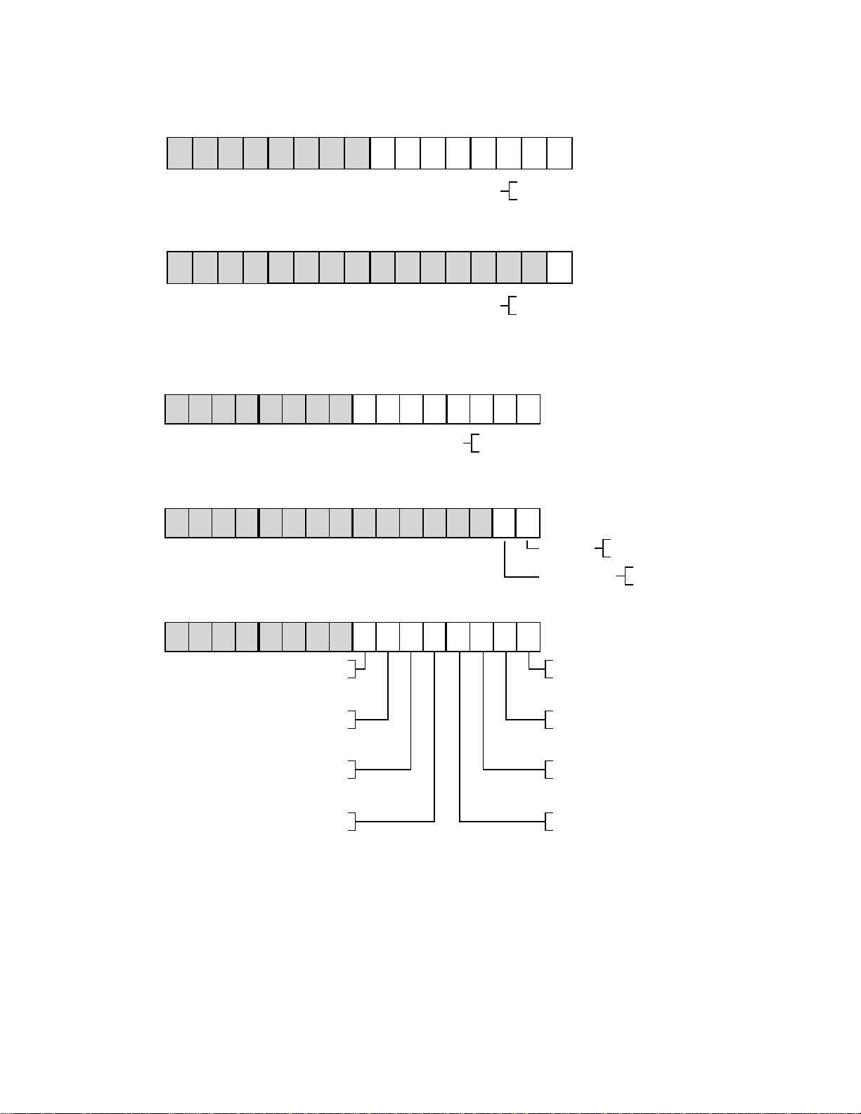
ADMC328
PIODIR0 (R/W)
15 14 13 12 11 10 9 8 7 6 5 4 3 2 1 0
0000000000000000
DM (0x2004)
PIO0 – PIO7
PIODIR1 (R/W)
15 14 13 12 11 10 9 8 7 6 5 4 3 2 1 0
PIODATA0 (R/W)
15 14 13 12 11 10 9 8 7 6 5 4 3 2 1 0
0000
15 14 13 12 11 10 9 8 7 6 5 4 3 2 1 0
00000000
15 14 13 12 11 10 9 8 7 6 5 4 3 2 1 0
0000
PIO0 – PIO7
PIODATA1 (R/W)
0000
PIOSELECT (R/W)
0 = INPUT
1 = OUTPUT
0 = INPUT
PIO8
1 = OUTPUT
0 = LOW LEVEL
1 = HIGH LEVEL
100
PIO8/AUX0 MODE
0000000000000000
DM (0x2005)
DM (0x2045)
PIO8 DATA
DM (0x2044)
0 = LO
1 = HI
0 = AUX0
1 = PIO8
0000
0 = CLKOUT
0 = AUX1
1 = PIO7
1 = PIO6
0 = RFS1
1 = PIO5
0 = DR1A
1 = PIO4
0000
11111111
DM (0x2049)
0 = TFS1
1 = PIO0
0 = DT1
1 = PIO1
0 = DR1B
1 = PIO2
0 = SCLK1
1 = PIO3
Figure 23. Configuration of PIO Registers
Default bit values are shown; if no value is shown, the bit field is undefined at reset. Reserved bits are shown on a gray field—these
bits should always be written as shown.
–26–
REV. B
PIOINTEN0 (R/W)
15 14 13 12 11 10 9 8 7 6 5 4 3 2 1 0
0000000000000000
ADMC328
DM (0x2006)
PIO0 – PIO7
PIOINTEN1 (R/W)
15 14 13 12 11 10 9 8 7 6 5 4 3 2 1 0
PIOFLAG0 (R)
15 14 13 12 11 10 9 8 7 6 5 4 3 2 1 0
00000000
PIO0 – PIO7
PIOFLAG1 (R)
15 14 13 12 11 10 9 8 7 6 5 4 3 2 1 0
00000000
0 = INTERRUPT DISABLE
1 = INTERRUPT ENABLE
0 = INTERRUPT DISABLE
PIO8
1 = INTERRUPT ENABLE
0 = NO INTERRUPT
1 = INTERRUPT FLAGGED
0 = NO INTERRUPT
PIO8
1 = INTERRUPT FLAGGED
0000000000000000
00000000
00000000
DM (0x2046)
DM (0x2007)
DM (0x2047)
Figure 24. Configuration of Additional PIO Registers
Default bit values are shown; if no value is shown, the bit field is undefined at reset. Reserved bits are shown on a gray field—these
bits should always be written as shown.
REV. B
–27–

ADMC328
AUXCH0 (R/W)
15 14 13 12 11 10 9 8 7 6 5 4 3 2 1 0
T
ON, AUX0
AUXCH1 (R/W)
15 14 13 12 11 10 9 8 7 6 5 4 3 2 1 0
T
ON, AUX1
AUXTM0 (R/W)
15 14 13 12 11 10 9 8 7 6 5 4 3 2 1 0
DM (0x2010)
0000000000000000
= 2 3 (AUXCH0) 3 t
0000000000000000
DM (0x2011)
= 2 3 (AUXCH1) 3 t
1111111100000000
DM (0x2012)
CK
CK
AUX0 PERIOD = 2 3 (AUXTM0 + 1) 3 t
AUXTM1 (R/W)
15 14 13 12 11 10 9 8 7 6 5 4 3 2 1 0
AUX1 PERIOD = 2 3 (1 + AUXTM1) 3
OFFSET = 2 3 (1 + AUXTM1) 3 t
1111111100000000
DM (0x2013)
CK
t
CK
CK
Figure 25. Configuration of AUX Registers
Default bit values are shown; if no value is shown, the bit field is undefined at reset. Reserved bits are shown on a gray field—these
bits should always be written as shown.
–28–
REV. B
ADMC328
15 14 13 12 11 10 9 8 7 6 5 4 3 2 1 0
ADC1 (R)
0000
ADC2 (R)
1514131211109876543210
0000 DM (0x2001)
ADC3 (R)
15 14 13 12 11 10 9 8 7 6 5 4 3 2 1 0
0000 DM (0x2002)
ADCAUX (R)
15 14 13 12 11 10 9 8 7 6 5 4 3 2 1 0
0000 DM (0x2003)
ICONST_TRIM (R/W)
15 14 13 12 11 10 9 8 7 6 5 4 3 2 1 0
0000000000000000
DM (0x2000)
DM (0x2068)
ICONST MIN = BITS 0 – 2 CLEARED.
ICONST MAX = BITS 0 – 2 SET.
Figure 26. Configuration of Additional AUX Registers
Default bit values are shown; if no value is shown, the bit field is undefined at reset. Reserved bits are shown on a gray field—these
bits should always be written as shown.
REV. B
–29–
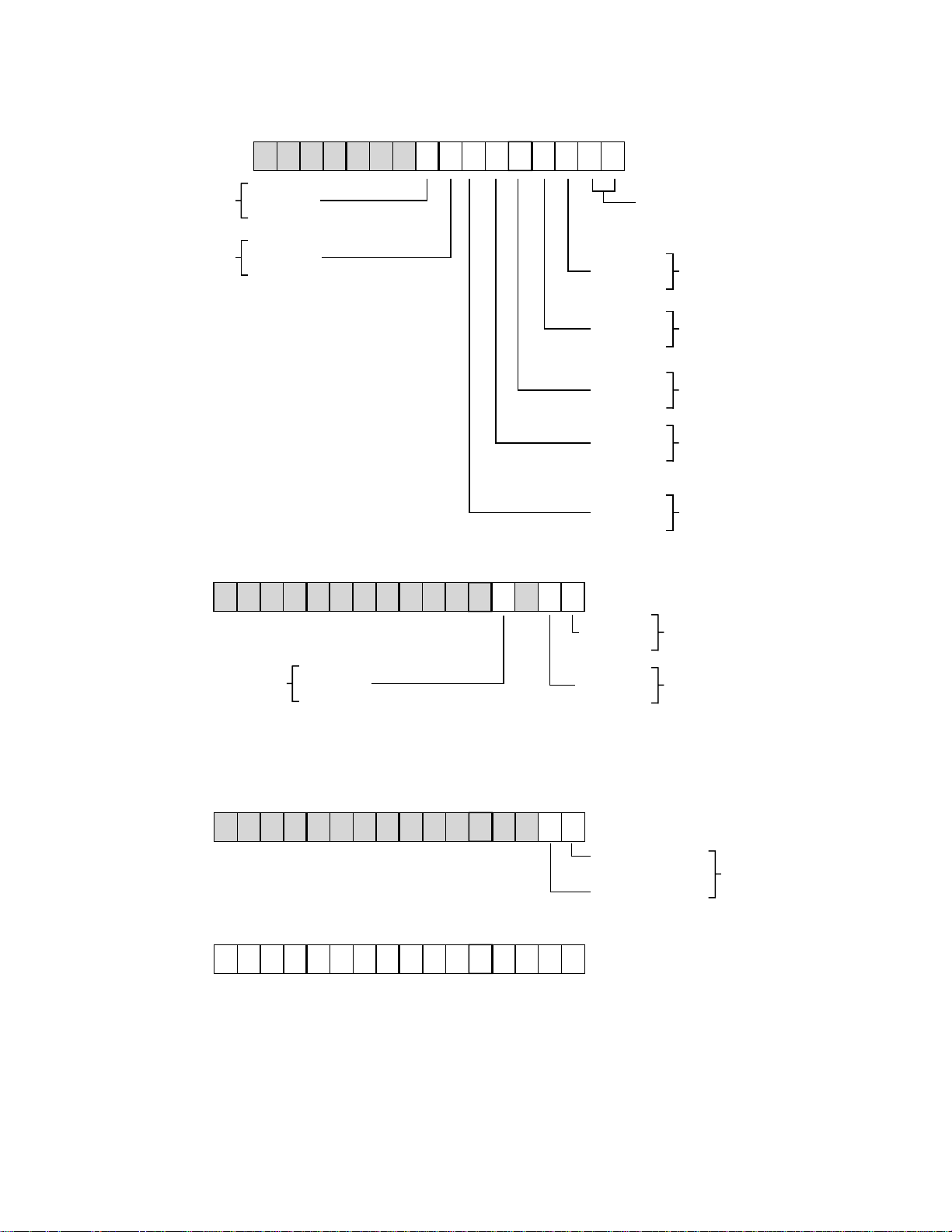
ADMC328
0 = OFFSET MODE
1 = INDEPENDENT MODE
0 = CLKIN RATE
1 = CLKOUT RATE
15 14 13 12 11 10 9 8 7 6 5 4 3 2 1 0
AUXILIARY
PWM SELECT
ADC
COUNTER
SELECT
15 14 13 12 11 10 9 8 7 6 5 4 3 2 1 0
MODECTRL (R/W)
SYSSTAT (R)
0000000000000000
00000000000
01
DM (0x2015)
ADC MUX CONTROL
00 VAUX0
01 VAUX1
10 VAUX2
11 VAUX3
PWMTRIP
INTERRUPT
PWMSYNC
INTERRUPT
SPORT1 DATA
RECEIVE
SELECT
SPORT1 MODE
SELECT
PWM UPDATE
MODE SELECT
DM (0x2016)
0 = DISABLE
1 = ENABLE
0 = DISABLE
1 = ENABLE
0 = DR1A
1 = DR1B
0 = SPORT
1 = UART
0 = SINGLE UPDATE MODE
1 = DOUBLE UPDATE MODE
0 = 1ST HALF OF PWM
CYCLE
1 = 2ND HALF OF PWM
CYCLE
15 14 13 12 11 10 9 8 7 6 5 4 3 2 1 0
15 14 13 12 11 10 9 8 7 6 5 4 3 2 1 0
PWM TIMER
STATUS
IRQFLAG (R)
000000000000
WDTIMER (W)
0000000000000000
PWMTRIP
PIN STATUS
WATCHDOG
STATUS
0000
DM (0x2017)
PWMTRIP INTERRUPT
PWMSYNC INTERRUPT
DM (0x2018)
0 = LOW
1 = HIGH
0 = NORMAL
1 = WATCHDOG RESET
OCCURRED
0 = NO INTERRUPT
1 = INTERRUPT
OCCURRED
Figure 27. Configuration of Status Registers
Default bit values are shown; if no value is shown, the bit field is undefined at reset. Reserved bits are shown on a gray field—these
bits should always be written as shown.
–30–
REV. B
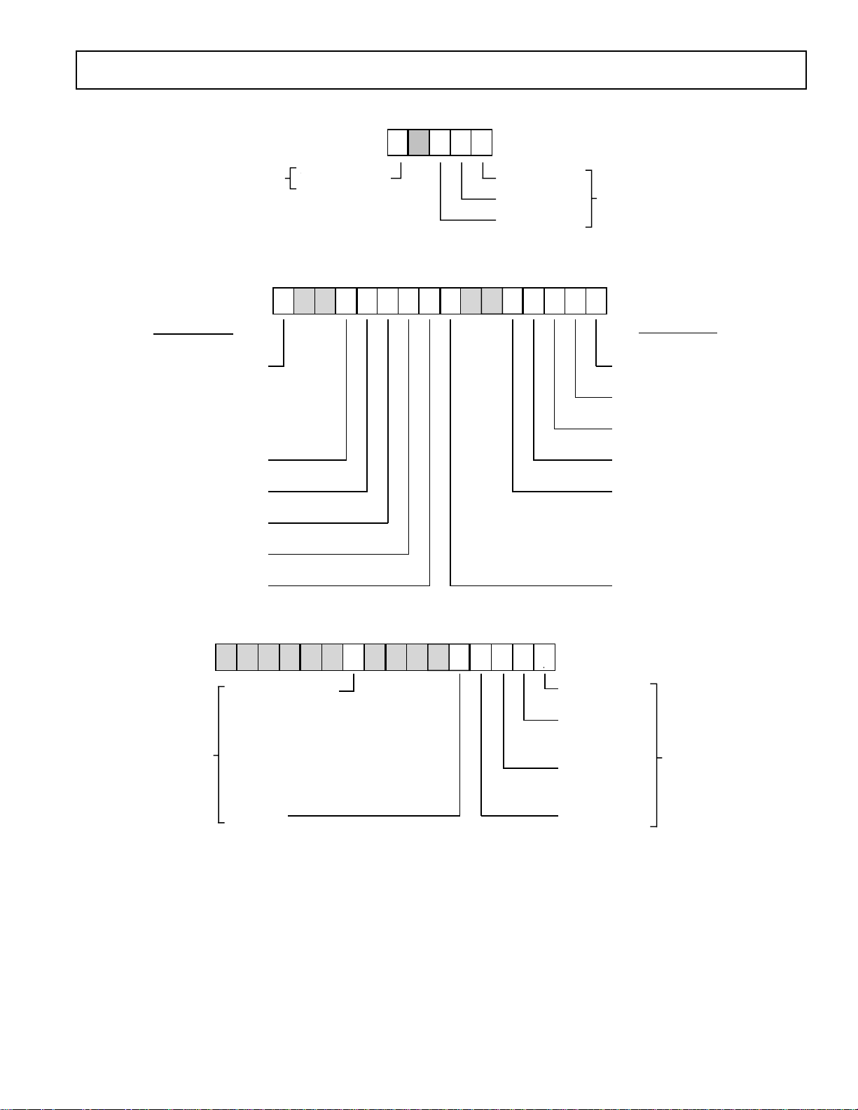
ICNTL
43210
00000
ADMC328
DSP REGISTER
0 = DISABLE
1 = ENABLE
INTERRUPT FORCE INTERRUPT CLEAR
IRQ2
SOFTWARE 1
SOFTWARE 0
SPORT1 TRANSMIT OR IRQ1
SPORT1 RECEIVE OR IRQ0
INTERRUPT NESTING
IFC
15 14 13 12 11 10 9 8 7 6 5 4 3 2 1 0
IRQ0 SENSITIVITY
IRQ1 SENSITIVITY
IRQ2 SENSITIVITY
0 = LEVEL
1 = EDGE
DSP REGISTER
0000000000000000
TIMER
SPORT1 RECEIVE OR IRQ0
SPORT1 TRANSMIT OR IRQ1
SOFTWARE 0
SOFTWARE 1
IRQ2
0 = DISABLE
(MASK)
1 = ENABLE
0 = DISABLE
(MASK)
1 = ENABLE
TIMER
IMASK (R/W)
15 14 13 12 11 10 9 8 7 6 5 4 3 2 1 0
0000000000000000
PERIPHERAL (OR IRQ2)
SOFTWARE 1
DSP REGISTER
TIMER
SPORT1 RECEIVE
(OR IRQ0)
SPORT1 TRANSMIT
(OR IRQ1)
SOFTWARE 0
Figure 28. Configuration of Interrupt Control Registers
Default bit values are shown; if no value is shown, the bit field is undefined at reset. Reserved bits are shown on a gray field—these
bits should always be written as shown.
REV. B
–31–

ADMC328
SYSCNTL (R/W)
SPORT1 CONFIGURE
MEMWAIT (R/W)
110000000101111
0 = FI, FO, IRQ0, IRQ1, SCLK
1 = SERIAL PORT
1111111111111111
DM (0x3FFF)
DM (0x3FFE)
0 = DISABLED
1 = ENABLED
15 14 13 12 11 10 9 8 7 6 5 4 3 2 1 0
0
SPORT1 ENABLE
15 14 13 12 11 10 9 8 7 6 5 4 3 2 1 0
Figure 29. Configuration of Registers
Default bit values are shown; if no value is shown, the bit field is undefined at reset. Reserved bits are shown on a gray field.
OUTLINE DIMENSIONS
Dimensions shown in inches and (mm).
28-Lead Plastic DIP
(N-28)
1.565 (39.70)
1.380 (35.10)
PIN 1
0.250
(6.35)
MAX
0.200 (5.05)
0.125 (3.18)
28
114
0.022 (0.558)
0.014 (0.356)
0.100
(2.54)
BSC
15
0.060 (1.52)
0.015 (0.38)
0.070
(1.77)
MAX
0.580 (14.73)
0.485 (12.32)
0.150
(3.81)
MIN
SEATING
PLANE
0.625 (15.87)
0.600 (15.24)
0.015 (0.381)
0.008 (0.204)
0.195 ( 4.95)
0.125 (3. 18)
C3429b–2.5–2/00 (rev. B)
28-Lead Wide-Body SOIC
0.7125 (18.10)
0.6969 (17.70)
28 15
PIN 1
0.0192 (0.49)
0.0118 (0.30)
0.0040 (0.10)
0.0500
(1.27)
BSC
0.0138 (0.35)
(R-28)
0.1043 (2.65)
0.0926 (2.35)
SEATING
PLANE
–32–
141
0.2992 (7.60)
0.2914 (7.40)
0.4193 (10.65)
0.0125 (0.32)
0.0091 (0.23)
0.3937 (10.00)
0.0291 (0.74)
0.0098 (0.25)
0.0500 (1.27)
88
08
0.0157 (0.40)
PRINTED IN U.S.A.
x 458
REV. B
 Loading...