

Page 1
High Performance DSP-Based
a
TARGET APPLICATIONS
Industrial Drives, Servo Drives, Variable Speed Drives,
Electric Vehicles
FEATURES
25 MIPS Fixed-Point DSP Core
Single Cycle Instruction Execution (40 ns)
ADSP-2100 Family Code Compatible
Independent Computational Units
ALU
Multiplier/Accumulator
Barrel Shifter
Multifunction Instructions
Single Cycle Context Switch
Powerful Program Sequencer
Zero Overhead Looping
Conditional Instruction Execution
Two Independent Data Address Generators
Memory Configuration
4K 24-Bit Program Memory RAM
2K 24-Bit Program Memory ROM
1K 16-Bit Data Memory RAM
High-Resolution Multichannel ADC System
Five Independent 16-Bit Sigma-Delta ADCs
76 dB SNR Typical (ENOB > 12 Bits)
Arranged in Two Independently Clocked Banks
Differential or Single-Ended Inputs
Programmable Sample Frequency to 32.5 kHz
Motor Controller
ADMC300
Flexible Synchronization of ADC and PWM Subsystems
Independent Offset Calibration for Each Channel
Two Dedicated ADC Interrupts
Internal 2.5 V Reference
Three Multiplexer Control Pins for External Expansion
Hardware or Software Convert Start
Individual Power-Down for Each Bank
Three-Phase PWM Generation Subsystem
16-Bit Dedicated PWM Generator
Edge Resolution to 40 ns
Programmable Dead Time
Programmable Minimum Pulsewidth
Double Update Mode Allows Duty Cycle
Adjustment on Half Cycle Boundaries
Special Features for Brushless DC Motors
Hardwired Polarity Control
External Dedicated Asynchronous Shutdown Pin
(PWMTRIP)
Additional Shutdown Pins in I/O System
Individual Enable/Disable of Each Output
High Frequency Chopping Mode
Transparent Transition to Overmodulation
Range with Duty Cycles of 100%
Programmable Interrupt Controller Manages Priority
and Masking of 11 Peripheral Interrupts
(Continued on Page 7)
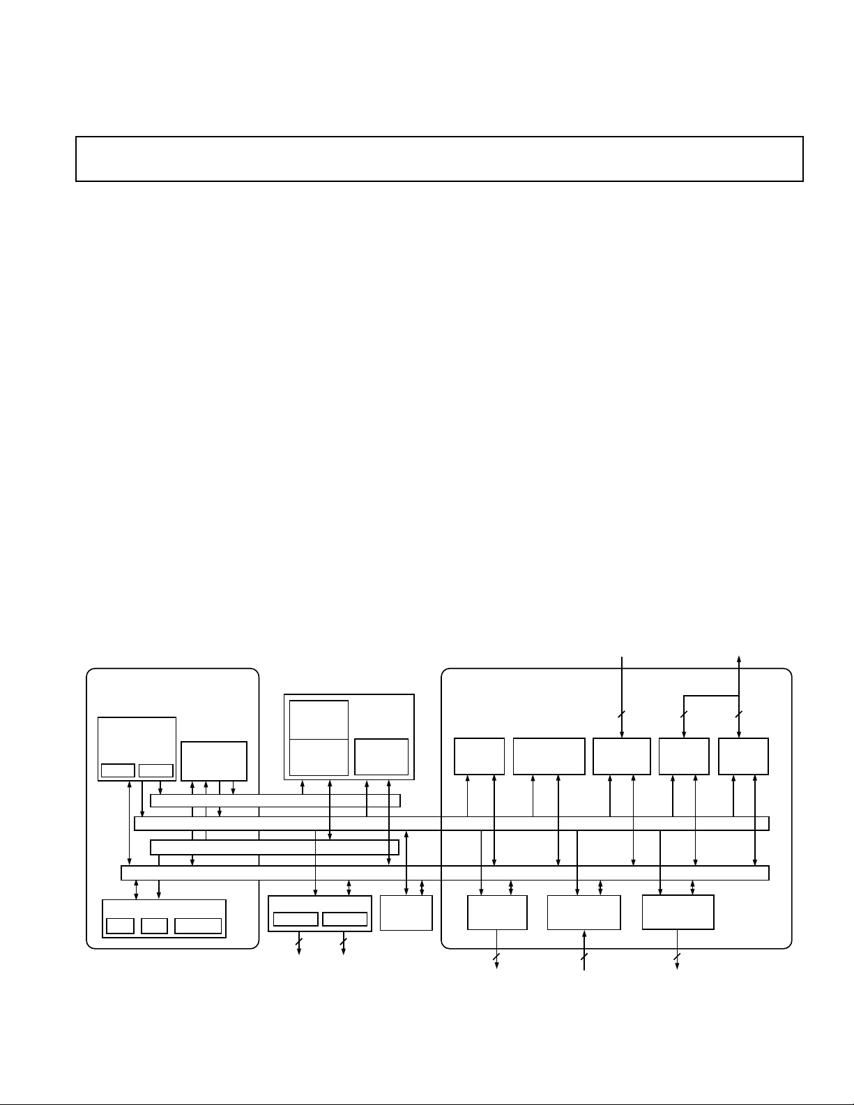
FUNCTIONAL BLOCK DIAGRAM
ADSP-2100 BASE
ARCHITECTURE
DATA
ADDRESS
GENERATORS
DAG 2
DAG 1
PROGRAM MEMORY ADDRESS BUS
DATA MEMORY ADDRESS BUS
PROGRAM MEMORY DATA BUS
DATA MEMORY DATA BUS
ARITHMETIC UNITS
ALU
MAC
PROGRAM
SEQUENCER
SHIFTER
PROGRAM
ROM
2K 24
PROGRAM
RAM
4K 24
SERIAL PORTS
SPORT 0
SPORT 1
56
MEMORY
DATA
RAM
1K 16
INTERVAL
TIMER
REV. B
Information furnished by Analog Devices is believed to be accurate and
reliable. However, no responsibility is assumed by Analog Devices for its
use, nor for any infringements of patents or other rights of third parties
which may result from its use. No license is granted by implication or
otherwise under any patent or patent rights of Analog Devices.
MOTOR CONTROL
PERIPHERALS
PWM
PROGRAM
INTERRUPT
CONTROLLER
SIGMA-DELTA
WATCH-
DOG
TIMER
AUXILIARY
One Technology Way, P.O. Box 9106, Norwood, MA 02062-9106, U.S.A.
Tel: 781/329-4700 World Wide Web Site: http://www.analog.com
Fax: 781/326-8703 © Analog Devices, Inc., 2000
3212
EVENT
CAPTURE
TIMERS
PWM
GENERATION
7102
ADCs
ENCODER
INTERFACE
DIGITAL
I/O
Page 2

ADMC300–SPECIFICATIONS
(VDD = AVDD = 5 V 10%, GND = AGND = 0 V, T
RECOMMENDED OPERATING CONDITIONS
CLKIN = 12.5 MHz, unless otherwise noted)
B Grade
Parameter Min Max Units
V
AV
T
DD
DD
AMB
Digital Supply Voltage 4.50 5.50 V
Analog Supply Voltage 4.50 5.50 V
Ambient Operating Temperature –40 +85 °C
ELECTRICAL CHARACTERISTICS
Parameter Test Conditions Min Max Unit
V
IH
V
IL
V
OH
V
OL
I
IH
I
IH
I
IH
I
IL
I
IL
I
IL
I
OZH
I
OZL
I
DD
I
DD
I
DD
I
DD
I
DD
I
DD
NOTES
1
Bidirectional pins: PIO0–PIO11, RFS0, RFS1, TFS0, TFS1, SCLK0, SCLK1.
2
Input only pins: PWMTRIP, PWMPOL, RESET, EIA, EIB, EIZP, DR1A, DR1B, DR0, CLKIN.
3
Output pins: PWMSYNC, CL, CH, BL, BH, AL, AH, MUX0–MUX2, AUX0, AUX1, CLKOUT, DT0, DT1.
4
Input only pins: RESET, EIA, EIB, EIZP, DR1A, DR1B, DR0, CLKIN.
5
Three-stateable pins: DT0, DT1, RFS0, RFS1, TFS0, TFS1, SCLK0, SCLK1.
6
Current reflects device operating with no output loads.
7
Dynamic condition refers to continuous operation of the DSP core, ADC banks and PWM generation in single update mode with PWMTM = 0x0480, ADCDIVA =
ADCDIVB = 0x180. The encoder inputs are quiescent.
8
Disabled refers to powering down both ADC banks and the internal reference generation circuit by setting Bits 10, 11 and 12 of the ADCCTRL register. Current is
total current from AVDD supply.
Specifications subject to change without notice.
Hi-Level Input Voltage1,
Lo-Level Input Voltage1,
Hi-Level Output Voltage1,
Lo-Level Output Voltage1,
Hi-Level Input Current
Hi-Level PWMTRIP, PIO0–PIO11 Current @ VDD = Max, 100 µA
Hi-Level PWMPOL Current @ VDD = Max, 10 µA
Lo-Level Input Current
Lo-Level PWMTRIP, PIO0–PIO11 Current @ VDD = Max, 10 µA
Lo-Level PWMPOL Current @ VDD = Max, 100 µA
Hi-Level Three-State Leakage Current
Lo-Level Three-State Leakage Current
Digital Power Supply Current (Dynamic)6,
Analog Power Supply Current (Disabled)
Analog Power Supply Current (Ref Only) @ AVDD = VDD = Max 6.5 mA
Analog Power Supply Current (Ref + BankA) @ AVDD = VDD = Max 11.0 mA
Analog Power Supply Current (Ref + BankB) @ AVDD = VDD = Max 13.0 mA
Analog Power Supply Current (Ref + BankA/B) @ AVDD = VDD = Max 18.0 mA
2
2
3
3
4
4
5
5
7
8
@ VDD = Max 2.0 V
@ VDD = Min 0.8 V
@ VDD = Min, 2.4 V
= –1.0 mA
I
OH
= Min, VDD – 0.3 V
@ V
DD
I
= –0.1 mA
OH
@ VDD = Min, 0.4 V
= 2.0 mA
I
OL
@ VDD = Max, 10 µA
V
= VDD Max
IN
V
= VDD Max
IN
= VDD Max
V
IN
@ VDD = Max, 10 µA
V
= 0 V
IN
V
= 0 V
IN
V
= 0 V
IN
@ VDD = Max, 10 µA
= VDD Max
V
IN
@ VDD = Max, 10 µA
V
= 0 V
IN
@ VDD = Max 100 mA
@ AVDD = VDD = Max 100 µA
= –40C to +85C,
AMB
–2–
REV. B
Page 3

ADMC300
ANALOG-TO-DIGITAL CONVERTER
(VDD = AVDD = 5 V 10%, GND = AGND = 0 V, V
CLKIN = 12.5 MHz, unless otherwise noted)
= 2.50 V, T
REFIN
= –40C to +85C,
AMB
Parameter Test Conditions Min Typ Max Unit
Signal-to-Noise Ratio
Total Harmonic Distortion
Common-Mode Rejection Ratio
Channel-Channel Crosstalk
1
(SNR) @VDD = 5.0 V, 72 76 dB
1
(THD) @ fS = 32.55 kHz, –70 dB
2
(CMRR) @ fIN = 1.017 kHz, –82 dB
3
ADCDIVn = 0x180, –76 dB
Gain Error V1–V5 = 4.0 V p-p 5 %
Gain V1N–V5N = V
V
IN
V
DIFF
V
OFFSET
f
MOD, MAX
f
S, MAX
Analog Input Range
Analog Input Voltage (Differential)
DC Offset Voltage
Maximum Sigma-Delta Modulator Rate ADCDIVA = 0x180 2.08 MHz
Maximum ADC Sample Rate
4
4
5
6
ADCDIVB = 0x180
ADCDIVA = 0x180 32.55 kHz
= 2.5 V 10,600 LSB/V
REFIN
0V
DD
VDD/2 V
55 mV
V
ADCDIVB = 0x180
V
REFIN
R
IN
NOTES
1
SNR measured with ADC channel configured in single-ended mode. SNR measurement does not include harmonic distortion, THD includes first six harmonics.
The effective number of bits (ENOB) is related to the SNR by SNR = 6.02 (ENOB) +1.76 dB. Input signal filtered at 1.5 kHz.
2
Input signal applied to both pins of input differential pair of ADC channel.
3
Input signal applied to four ADC channels, dc applied to fifth, measurement taken at fifth ADC channel.
4
Peak-peak input voltage in differential input configuration is half that in single-ended mode.
5
This offset may be corrected for, using the ADC calibration feature.
6
At maximum sigma-delta modulator rate of 2.08 MHz.
7
Input reference pins: REFINA, REFINB.
8
Analog signal input pins: V1–V5, V1N–V5N.
Specifications subject to change without notice.
Reference Input Voltage
Equivalent Input Resistance
7
8
2.4 2.5 2.6 V
25 kΩ
VOLTAGE REFERENCE
(VDD = AVDD = 5 V 10%, GND = AGND = 0 V, T
noted)
= –40C to +85C, CLKIN = 12.5 MHz, unless otherwise
AMB
Parameter Test Conditions Min Typ Max Unit
V
REF
Voltage Level 2.25 2.75 V
Source Current –100 µA
Power Supply Rejection Ratio (PSRR) –5 5 mV/V
Specifications subject to change without notice.
(V
PULSEWIDTH MODULATOR
= AVDD = 5 V 10%, GND = AGND = 0 V, T
DD
otherwise noted)
= –40C to +85C, CLKIN = 12.5 MHz, unless
AMB
Parameter Test Conditions Min Typ Max Unit
Counter Resolution
1
16 Bits
Edge Resolution Double Update Mode 40 ns
T
D
Programmable Dead Time 0 81.84 µs
Programmable Dead Time Increments 80 ns
T
MIN
f
PWM
T
SYNC
f
CHOP
NOTES
1
Resolution varies with PWM switching frequency, 191 Hz = 16 bits, 3.05 kHz = 12 bits, 48.8 kHz = 8 bits (12.5 MHz CLKIN) in single update mode.
Specifications subject to change without notice.
Programmable Pulse Deletion 0 40.92 µs
Programmable Deletion Increments 40 ns
PWM Frequency Range
1
191 Hz
PWMSYNC Pulsewidth 0.04 10.24 µs
Gate Drive Chop Frequency 0.0244 6.25 MHz
–3–REV. B
Page 4

ADMC300–SPECIFICATIONS
(VDD = AVDD = 5 V 10%, GND = AGND = 0 V, T
ENCODER INTERFACE UNIT
otherwise noted)
Parameter Test Conditions Min Typ Max Unit
f
ENC, MAX
NOTES
1
Assumes perfect quadrature encoder signals.
Specifications subject to change without notice.
Maximum Encoder Pulse Rate
1
(VDD = AVDD = 5 V 10%, GND = AGND = 0 V, T
AUXILIARY PWM OUTPUTS
otherwise noted)
Parameter Test Conditions Min Typ Max Unit
Resolution 8 Bits
f
AUXPWM
Specifications subject to change without notice.
Switching Frequency 48.8 kHz
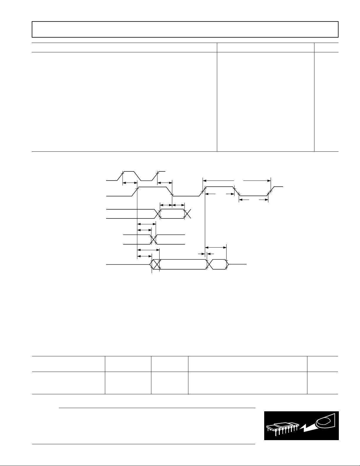
TIMING PARAMETERS
Parameter Min Max Unit
Clock Signals
t
is defined as 0.5 t
CK
to half the instruction rate; a 12.5 MHz input clock (which is equivalent to 80 ns)
yields a 40 ns processor cycle (equivalent to 25 MHz). t
0.5 t
period should be substituted for all relevant timing parameters to obtain
CKI
specification value.
Example: t
= 0.5 tCK – 10 ns = 0.5 (40 ns) – 10 ns = 10 ns.
CKH
Timing Requirements:
t
CKI
t
CKIL
t
CKIH
CLKIN Period 80 150 ns
CLKIN Width Low 20 ns
CLKIN Width High 20 ns
Switching Characteristics:
t
CKL
t
CKH
t
CKOH
CLKOUT Width Low 0.5 tCK – 10 ns
CLKOUT Width High 0.5 tCK – 10 ns
CLKIN High to CLKOUT High 0 20 ns
Control Signals
Timing Requirement:
t
RSP
RESET Width Low 5 t
PWM Shutdown Signals
Timing Requirements:
t
PWMTPW
t
PIOPWM
NOTES
1
Applies after power-up sequence is complete. Internal phase lock loop requires no more than 2000 CLKIN cycles assuming stable CLKIN (not including crystal
oscillator start-up time).
Specifications subject to change without notice.
PWMTRIP Width Low 3 t
PIO Width Low 3 t
. The ADMC300 uses an input clock with a frequency equal
CKI
values within the range of
CK
t
CKI
= –40C to +85C, CLKIN = 12.5 MHz, unless
AMB
3.1 MHz
= –40C to +85C, CLKIN = 12.5 MHz, unless
AMB
1
CK
CK
CK
t
CKIH
ns
ns
ns
CLKIN
CLKOUT
t
CKIL
t
CKL
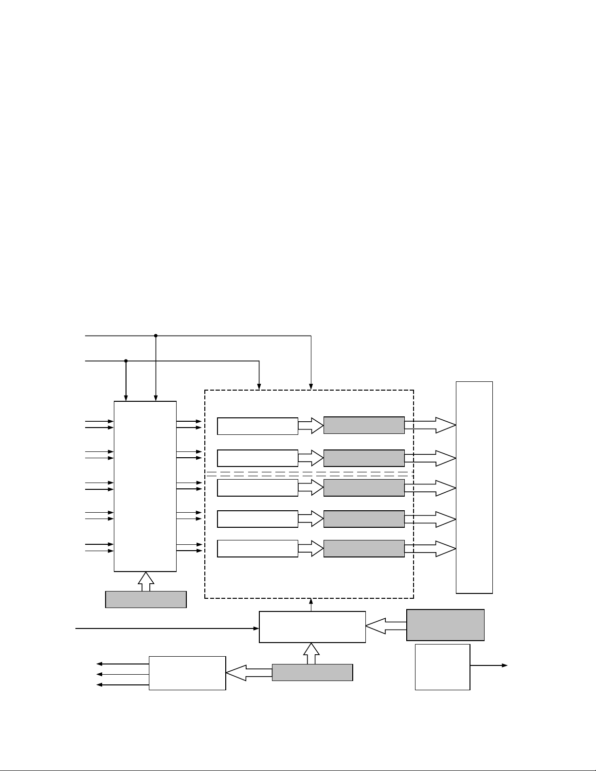
Figure 1. Clock Signals
–4–
t
CKOH
t
CKH
REV. B
Page 5
ADMC300
WARNING!
ESD SENSITIVE DEVICE
Parameter Min Max Unit
Serial Ports
Timing Requirements:
t
SCK
t
SCS
t
SCH
t
SCP
Switching Characteristics:
t
CC
t
SCDE
t
SCDV
t
RH
t
RD
t
SCDH
t
SCDD
Specifications subject to change without notice.
SCLK Period 50 ns
DR/TFS/RFS Setup before SCLK Low 5 ns
DR/TFS/RFS Hold after SCLK Low 10 ns
SCLKIN Width 20 ns
CLKOUT High to SCLK
OUT
0.25 t
CK
0.25 tCK + 15 ns
SCLK High to DT Enable 0 ns
SCLK High to DT Valid 20 ns
TFS/RFS
TFS/RFS
Hold after SCLK High 0 ns
OUT
Delay from SCLK High 20 ns
OUT
DT Hold after SCLK High 0 ns
SCLK High to DT Disable 20 ns
CLKOUT
SCLK
RFS
TFS
RFS
TFS
DR
OUT
OUT
DT
IN
IN
t
CC
t
SCDV
t
SCDE
t
CC
t
SCStSCH
t
RD
t
RH
Figure 2. Serial Ports
ABSOLUTE MAXIMUM RATINGS*
Supply Voltage (VDD) . . . . . . . . . . . . . . . . . . –0.3 V to +7.0 V
Supply Voltage (AV
Input Voltage . . . . . . . . . . . . . . . . . . . . –0.3 V to V
Output Voltage Swing . . . . . . . . . . . . . –0.3 V to V
) . . . . . . . . . . . . . . . . .–0.3 V to +7.0 V
DD
+ 0.3 V
DD
+ 0.3 V
DD
Operating Temperature Range (Ambient) . . . –40°C to +85°C
t
SCK
t
SCP
t
SCP
t
SCDD
t
SCDH
Storage Temperature Range . . . . . . . . . . . . –65°C to +150°C
Lead Temperature (5 sec) . . . . . . . . . . . . . . . . . . . . . .+280°C
*Stresses greater than those listed above may cause permanent damage to the
device. These are stress ratings only; functional operation of the device at these
or any other conditions greater than those indicated in the operational sections of
this specification is not implied. Exposure to absolute maximum rating conditions
for extended periods may affect device reliability.
ORDERING GUIDE
Temperature Instruction Package Package
Model Range Rate Description Option
ADMC300BST –40°C to +85°C 25 MHz 80-Lead Plastic Thin Quad Flatpack (TQFP) ST-80
ADMC300-ADVEVALKIT Development Tool Kit
ADMC300-PB Evaluation/Processor Board
CAUTION
ESD (electrostatic discharge) sensitive device. Electrostatic charges as high as 4000 V readily
accumulate on the human body and test equipment and can discharge without detection.
Although the ADMC300 features proprietary ESD protection circuitry, permanent damage may
occur on devices subjected to high-energy electrostatic discharges. Therefore, proper ESD
precautions are recommended to avoid performance degradation or loss of functionality.
–5–REV. B
Page 6
ADMC300
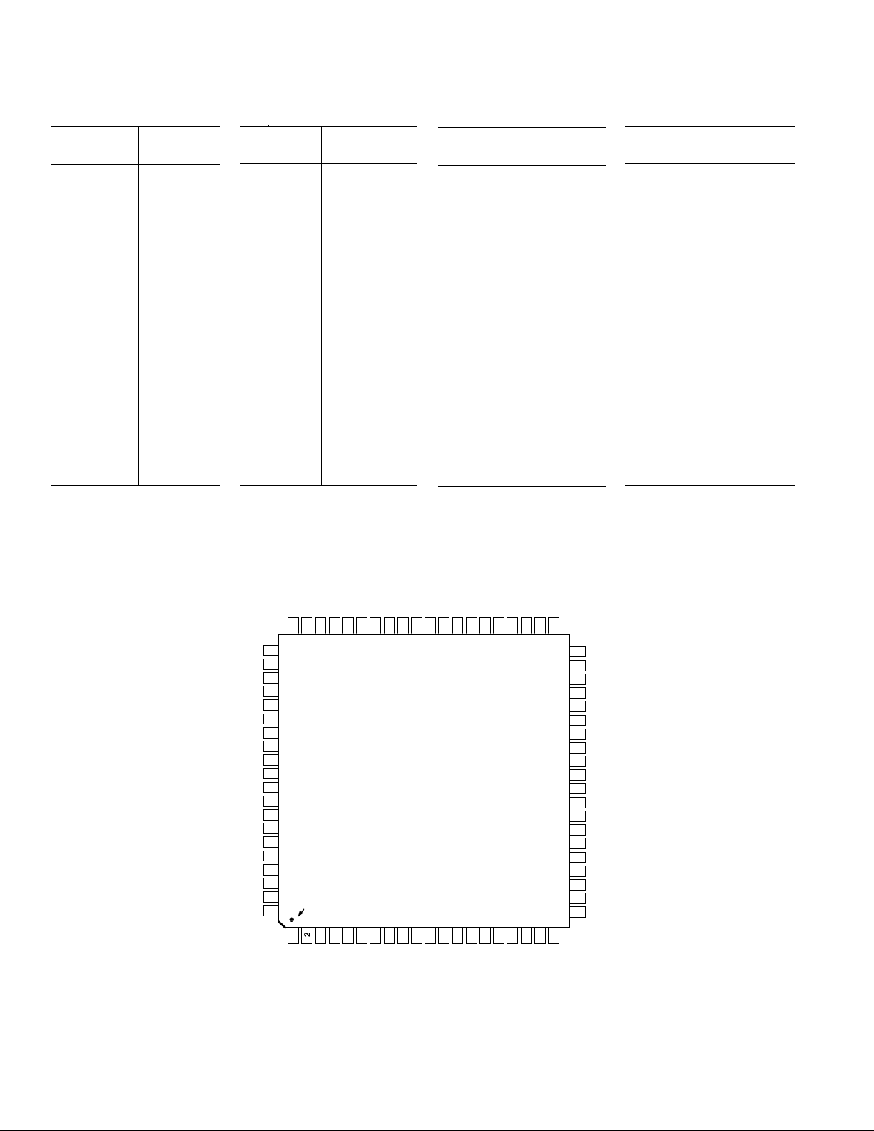
PIN FUNCTION DESCRIPTIONS
Pin Pin Pin
No. Type Name
1GNDGND
2I DR0
3 O DT0
4 I/O RFS0
5 I/O TFS0
6 I/O SCLK0
7 SUP V
DD
8GNDGND
9I PWMTRIP
10 O PWMSYNC
11 O CL
12 O CH
13 O BL
14 GND GND
15 SUP V
DD
16 O BH
17 O AL
18 O AH
19 O MUX0
20 O MUX1
Pin Pin Pin
No. Type Name
21 O MUX2
22 GND GND
23 SUP V
DD
24 O AUX0
25 O AUX1
26 I/O PIO0
27 I/O PIO1
28 I/O PIO2
29 I/O PIO3
30 I/O PIO4
31 GND GND
32 SUP V
DD
33 I/O PIO5
34 I/O PIO6
35 I/O PIO7
36 I/O PIO8
37 I/O PIO9/CONVST
38 I/O PIO10/ETU0
39 I/O PIO11/ETU1
40 GND AGND
PIN CONFIGURATION
80-Lead Plastic Thin Quad Flatpack (TQFP)
(ST-80)
Pin Pin Pin
No. Type Name
41 SUP AV
DD
42 I V5N
43 I V5
44 I V4N
45 I V4
46 I V3N
47 I V3
48 SUP AV
DD
49 GND AGND
50 GND AGND
51 SUP AV
DD
52 I REFINB
53 I REFINA
54 O VREF
55 I V2N
56 I V2
57 I V1N
58 I V1
59 SUP AV
DD
60 GND AGND
Pin Pin Pin
No. Type Name
61 GND GND
62 GND GND
63 I EIZP
64 I EIA
65 I EIB
66 I RESET
67 I PWMPOL
68 GND GND
69 I CLKIN
70 O XTAL
71 O CLKOUT
72 GND GND
73 SUP V
DD
74 I DR1A
75 I DR1B
76 O DT1
77 I/O RFS1/SROM
78 I/O TFS1
79 I/O SCLK1
80 SUP V
DD
GND
GND
EIZP
EIA
EIB
RESET
PWMPOL
GND
CLKIN
XTAL
CLKOUT
GND
V
DR1A
DR1B
DT1
RFS1/SROM
TFS1
SCLK1
V
DD
AV
AGND
59
60
61
62
63
64
65
66
67
68
69
70
71
72
DD
73
74
75
76
77
78
PIN 1
79
DD
IDENTIFIER
80
2
1
DR0
GND
V1
58
3
DT0
V1N
57
4
RFS0
V2
56
5
TFS0
V2N
545552
7
6
V
SCLK0
REFINB
REFINA
VREF
535051
ADMC300
TOP VIEW
(Not to Scale)
8
9
DD
GND
PWMTRIP
DD
AGND
AGND
AV
49
11
10
12
CL
CH
PWMSYNC
V4N
17
AL
V5
434442
18
AH
V5N
19
MUX0
DD
AV
41
20
MUX1
40
AGND
39
PIO11/ETU1
38
PIO10/ETU0
PIO9/CONVST
37
PIO8
36
PIO7
35
PIO6
34
33
PIO5
V
32
DD
GND
31
30
PIO4
PIO3
29
PIO2
28
PIO1
27
PIO0
26
AUX1
25
AUX0
24
V
23
DD
GND
22
MUX2
21
V3N
V3
AV
V4
46
48
45
47
14
15
13
16
DD
BL
BH
V
GND
DD
–6–
REV. B
Page 7

ADMC300
(Continued from Page 1)
Flexible Encoder Interface Subsystem
Incremental Encoder Interface
Dedicated Three Pin Interface (EIA, EIB, EIZP)
16-Bit Quadrature Counter
Input Encoder Signals to 3.1 MHz
Optional Use of Zero Marker to Reset Counter
Single North Marker Mode—Permits Single
Reset of Counter On Only First Zero Marker
Status Bits to Read Encoder Inputs
Companion Encoder Event System for Accuracy
Enhancements at Low Speeds
Associated EIU Loop Timer Permits Regular,
Programmable Updating of All Encoder and
Event Timer Registers
EIU Timer Can Also Be Used as General Purpose
Timer If Not Linked to EIU Block
Peripheral I/O (PIO) Subsystem
12-Pin Digital I/O Port
Bit Configurable as Input or Output
Each Pin Configurable as Rising Edge, Falling Edge,
High Level or Low Level Interrupt
Four Dedicated PIO Interrupts for PIO0 to PIO3
One Combined Interrupt for PIO4 to PIO11
Each I/O Line Configurable as PWM Trip Source
Two 8-Bit Auxiliary PWM Outputs
Synthesized Analog Output
Fixed 48.8 kHz Operation
0 to 99.6% Duty Cycle
Event Timer Unit
Two Event Timer Channels with Dedicated Event
Capture Blocks
Permits Timing of Duty-Cycle, Period and Frequency
Configurable Event Definition
Dedicated Event Timer Interrupt
Event Timer Readable On-the-Fly
16-Bit Watchdog Timer
Programmable 16-Bit Interval Timer with Prescaler
Two Double Buffered Synchronous Serial Ports
Four Boot Load Protocols via SPORT1
2
PROM/SROM Booting
E
UART Booting (SCI Compatible) with Autobaud
Feature
Synchronous Master Booting with Autobaud Feature
Synchronous Slave Booting with Autobaud Feature
Debugger Interface via SPORT1 with Autobaud (UART
and Synchronous Supported)
ROM Utilities
Full Debugger for Program Development
Preprogrammed Math Functions
Preprogrammed Motor Control Functions—Vector
Transformations
80-Lead TQFP Package
Industrial Temperature Range –40C to +85C
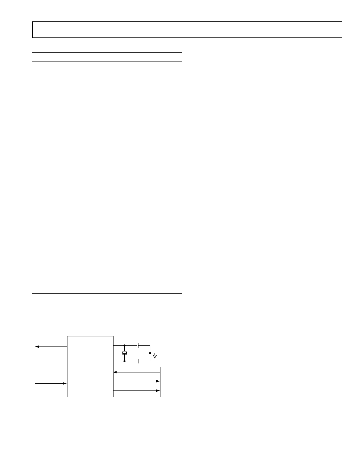
GENERAL DESCRIPTION
The ADMC300 is a single-chip DSP-based controller, suitable
for high performance control of ac induction motors, permanent
magnet synchronous motors and brushless dc motors. The
ADMC300 integrates a 25 MIPS, fixed-point DSP core with a
complete set of motor control peripherals that permits fast,
efficient development of servo motor controllers.
The DSP core of the ADMC300 is the ADSP-2171, which is
completely code compatible with the ADSP-2100 DSP family
and combines three computational units, data address generators and a program sequencer. The computational units comprise an ALU, a multiplier/accumulator (MAC) and a barrel
shifter. The ADSP-2171 adds new instructions for bit manipulation, multiplication (X squared), biased rounding and global
interrupt masking. In addition, two flexible, double-buffered,
bidirectional, synchronous serial ports are included in the
ADMC300.
The ADMC300 provides 4K × 24-bit program memory RAM,
2K × 24-bit program memory ROM and 1K × 16-bit data
memory RAM. The program and data memory RAM can be
boot loaded through the serial port from either a serial SROM/
2
E
PROM, asynchronous (UART) connection, or synchronous connection. The program memory ROM includes a
monitor that adds software debugging features through the
serial port. In addition, a number of pre-programmed mathematical and motor control functions are included in the
program memory ROM.
The motor control peripherals of the ADMC300 comprise a
high performance, five channel ADC system that uses sigmadelta conversion technology offering a typical signal-to-noise
ratio (SNR) of 76 dB, equivalent to 12 bits. In addition, a 16-bit
center-based PWM generation unit can be used to produce high
accuracy PWM signals with minimal processor overhead. The
ADMC300 also contains a flexible encoder interface unit for
position sensor feedback, two auxiliary PWM outputs, twelve
lines of digital I/O, a two-channel event capture system, a 16-bit
watchdog timer, a 16-bit interval timer and a programmable
interrupt controller that manages all peripheral interrupts.
–7–REV. B
Page 8
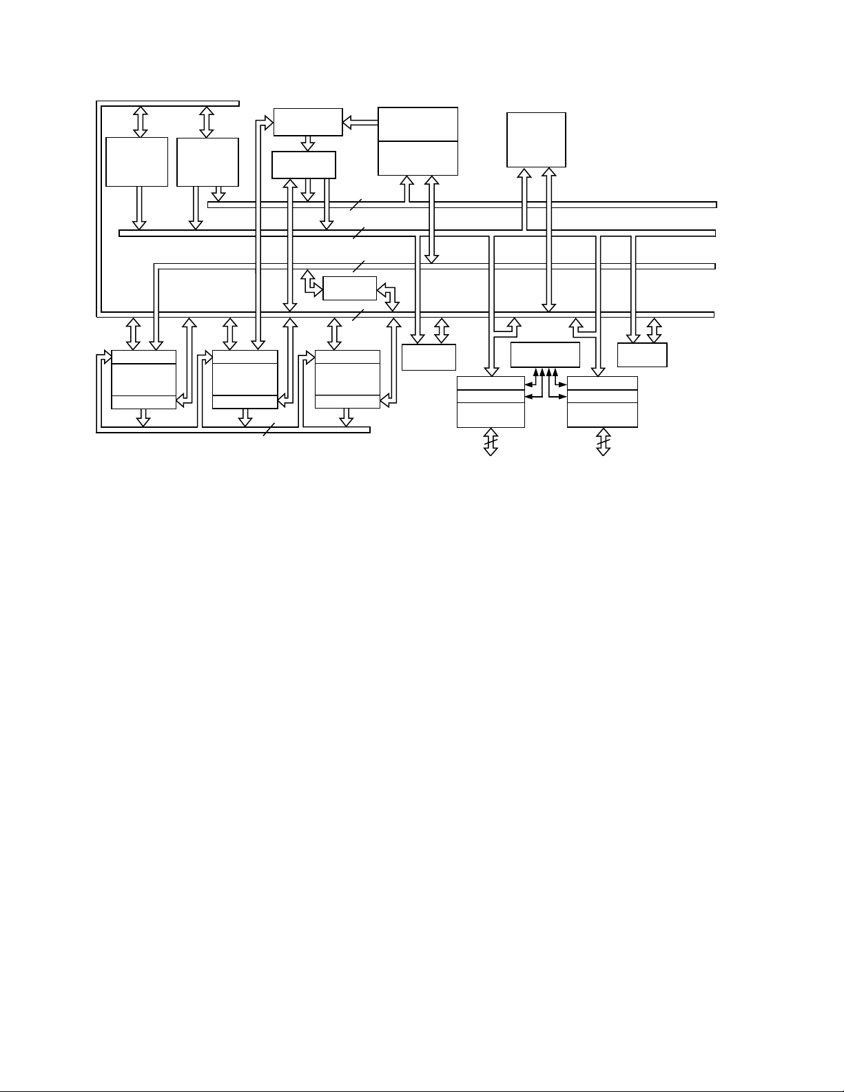
ADMC300
DATA
ADDRESS
GENERATOR
#1
INPUT REGS
ALU
OUTPUT REGS
DATA
ADDRESS
GENERATOR
#2
INPUT REGS
OUTPUT REGS
MAC
INSTRUCTION
PROGRAM
SEQUENCER
16
R BUS
REGISTER
OUTPUT REGS
14
14
24
BUS
EXCHANGE
16
INPUT REGS
SHIFTER
PM ROM
2K 24
PM RAM
4K 24
CONTROL
LOGIC
PMA BUS
DMA BUS
PMD BUS
DMD BUS
TRANSMIT REG
RECEIVE REG
Figure 3. DSP Core Block Diagram
SERIAL
PORT 0
5
DM RAM
1K 16
COMPANDING
CIRCUITRY
TRANSMIT REG
RECEIVE REG
SERIAL
PORT 1
6
TIMER
DSP CORE ARCHITECTURE OVERVIEW
Figure 3 is an overall block diagram of the DSP core of the
ADMC300, which is based on the fixed-point ADSP-2171. The
ADSP-2171 flexible architecture and comprehensive instruction
set allows the processor to perform multiple operations in parallel. In one processor cycle (40 ns with a 12.5 MHz CLKIN) the
DSP core can:
• Generate the next program address.
• Fetch the next instruction.
• Perform one or two data moves.
• Update one or two data address pointers.
• Perform a computational operation.
This all takes place while the processor continues to:
• Receive and transmit through the serial ports.
• Decrement the interval timer.
• Generate PWM signals.
• Convert the ADC input signals.
• Operate the encoder interface unit.
• Operate all other peripherals including the auxiliary PWM and
event timer subsystem.
The processor contains three independent computational units:
the arithmetic and logic unit (ALU), the multiplier/accumulator
(MAC) and the shifter. The computational units process 16-bit
data directly and have provisions to support multiprecision
computations. The ALU performs a standard set of arithmetic
and logic operations; division primitives are also supported.
The MAC performs single-cycle multiply, multiply/add, multiply/
subtract operations with 40 bits of accumulation. The shifter
performs logical and arithmetic shifts, normalization, denormalization, and derive exponent operations. The shifter can be used
to efficiently implement numeric format control including floatingpoint representations.
The internal result (R) bus directly connects the computational
units so that the output of any unit may be the input of any unit
on the next cycle.
A powerful program sequencer and two dedicated data address
generators ensure efficient delivery of operands to these computational units. The sequencer supports conditional jumps and
subroutine calls and returns in a single cycle. With internal loop
counters and loop stacks, the ADMC300 executes looped code
with zero overhead; no explicit jump instructions are required
to maintain the loop.
–8–
REV. B
Page 9

ADMC300
Two data address generators (DAGs) provide addresses for
simultaneous dual operand fetches from data memory and
program memory. Each DAG maintains and updates four
address pointers (I registers). Whenever the pointer is used to
access data (indirect addressing), it is post-modified by the
value in one of four modify (M) registers. A length value may
be associated with each pointer (L registers) to implement
automatic modulo addressing for circular buffers. The circular
buffering feature is also used by the serial ports for automatic
data transfers to and from on-chip memory. DAG1 generates
only data memory address but provides an optional bit-reversal
capability. DAG2 may generate either program or data memory
addresses, but has no bit-reversal capability.
Efficient data transfer is achieved with the use of five internal
buses:
• Program Memory Address (PMA) Bus
• Program Memory Data (PMD) Bus
• Data Memory Address (DMA) Bus
• Data Memory Data (DMD) Bus
• Result (R) Bus
Program memory can store both instructions and data, permitting the ADMC300 to fetch two operands in a single cycle—
one from program memory and one from data memory. The
ADMC300 can fetch an operand from on-chip program memory
and the next instruction in the same cycle.
The ADMC300 writes data from its 16-bit registers to the 24-bit
program memory using the PX register to provide the lower
eight bits. When it reads data (not instructions) from 24-bit
program memory to a 16-bit data register, the lower eight bits
are placed in the PX register.
The ADMC300 can respond to a number of distinct DSP core
and peripheral interrupts. The DSP core interrupts include
serial port receive and transmit interrupts, timer interrupts,
software interrupts and external interrupts. The motor control
peripherals also produce interrupts to the DSP core.
The two serial ports (SPORTs) provide a complete synchronous serial interface with optional companding in hardware and
a wide variety of framed and unframed data transmit and receive modes of operation. Each SPORT can generate an internal programmable serial clock or accept an external serial clock.
Boot loading of both the program and data memory RAM of
the ADMC300 is through the serial port SPORT1.
A programmable interval counter is also included in the DSP
core and can be used to generate periodic interrupts. A 16-bit
count register (TCOUNT) is decremented every n processor
cycles, where n–1 is a scaling value stored in the 8-bit TSCALE
register. When the value of the counter reaches zero, an interrupt
is generated and the count register is reloaded from a 16-bit
period register (TPERIOD).
The ADMC300 instruction set provides flexible data moves
and multifunction (one or two data moves with a computation)
instructions. Each instruction is executed in a single 40 ns
processor cycle (for a 12.5 MHz CLKIN). The ADMC300
assembly language uses an algebraic syntax for ease of coding
and readability. A comprehensive set of development tools
support program development. For further information on the
DSP core, refer to the ADSP-2100 Family User’s Manual, Third
Edition, with particular reference to the ADSP-2171.
Serial Ports
The ADMC300 incorporates two complete synchronous serial
ports (SPORT0 and SPORT1) for serial communication and
multiprocessor communication. Following is a brief list of capabilities of the ADMC300 SPORTs. Refer to the ADSP-2100
Family User’s Manual, Third Edition, for further details.
• SPORTs are bidirectional and have a separate, doublebuffered transmit and receive section.
• SPORTs can use an external serial clock or generate their
own serial clock internally.
• SPORTs have independent framing for the receive and
transmit sections. Sections run in a frameless mode or with
frame synchronization signals internally or externally generated.
Frame synchronization signals are active high or inverted, with
either of two pulsewidths and timings.
• SPORTs support serial data word lengths from 3 bits to 16
bits and provide optional A-law and µ-law companding ac-
cording to ITU (formerly CCITT) recommendation G.711.
• SPORT receive and transmit sections can generate unique
interrupts on completing a data word transfer.
• SPORTs can receive and transmit an entire circular buffer of
data with only one overhead cycle per data word. An interrupt is generated after a data buffer transfer.
• SPORT0 has a multichannel interface to selectively receive
and transmit a 24-word or 32-word, time-division multiplexed, serial bitstream.
• SPORT1 can be configured to have two external interrupts
(IRQ0 and IRQ1), and the Flag In and Flag Out signals.
The internally generated serial clock may still be used in this
configuration.
• SPORT1 is the default input for program and data memory
boot loading. The RFS1 pin can be configured internal to
the ADMC300 as an SROM/E
• SPORT1 has two data receive pins (DR1A and DR1B). The
DR1A pin is intended for synchronous boot loading from the
external SROM/E
the data receive pin for boot loading from an external UART
(SCI compatible) or synchronous connection, as the data
receive pin for the debugger communicating over the
debugger interface, or as the data receive pin for a general
purpose SPORT after booting. These two pins are internally
multiplexed onto the one DR1 port of the SPORT. The particular data receive pin selected is determined by a bit in the
MODECTRL register.
2
PROM. The DR1B pin can be used as
2
PROM reset signal.
–9–REV. B
Page 10

ADMC300
PIN FUNCTION DESCRIPTION
The ADMC300 is available in an 80-lead TQFP package. Table I
contains the pin descriptions.
Table I. Pin List
Pin #
Group of Input/
Name Pins Output Function
RESET 1 I Processor Reset Input.
SPORT0 5 I/O Serial Port 0 Pins (TFS0, RFS0,
DT0, DR0, SCLK0).
SPORT1 6 I/O Serial Port 1 Pins (TFS1,
RFS1, DT1, DR1A, DR1B,
SCLK1).
CLKOUT 1 O Processor Clock Output.
CLKIN, XTAL 2 I, O External Clock or Quartz Crystal
Connection Point.
PIO0–PIO11 12 I/O Digital I/O Port, External Con-
vert Start and Event Timer
Pins.
AUX0–AUX1 2 O Auxiliary PWM Outputs.
AH–CL 6 O PWM Outputs.
PWMTRIP 1 I PWM Trip Signal.
PWMPOL 1 I PWM Polarity Pin.
PWMSYNC 1 O PWM Synchronization Pin.
V1–V5 5 I Noninverting Inputs of the Dif-
ferential ADCs’ Input Amplifiers.
V1N–V5N 5 I Inverting Inputs of the Differen-
tial ADCs’ Input Amplifiers.
REFINA– 2 I Voltage reference inputs for
REFINB ADCs.
VREF 1 O Voltage Reference Output.
MUX0–MUX2 3 O Multiplexer Control Lines.
EIA, EIB, EIZP 3 I Encoder Interface Pins.
AV
DD
AGND 4 Analog Ground.
V
DD
GND 9
INTERRUPT OVERVIEW
4 Analog Power Supply.
6 Digital Power Supply.
Digital Ground.
The ADMC300 can respond to nineteen different interrupt
sources, eight of which are internal DSP core interrupts and
eleven interrupts from the motor control peripherals. The eight
DSP core interrupts comprise the peripheral (IRQ2), SPORT0
receive, SPORT0 transmit, SPORT1 receive (or IRQ0), SPORT1
transmit (or IRQ1), two software and the interval timer interrupts.
In addition, the motor control peripherals add eleven interrupts
that include two ADC, two PWM, five peripheral I/O, one encoder interface and one event timer interrupt. The interrupts are
internally prioritized and individually maskable. All peripheral
interrupts are multiplexed into the DSP core through the peripheral IRQ2 interrupt. The programmable interrupt controller
manages the masking and vector addressing of all eleven peripheral interrupts. A detailed description of the operation of the
entire interrupt system of the ADMC300 is given later, after a
more detailed description of the various peripheral systems.
Windows is a registered trademark of Microsoft Corporation.
–10–
Memory Map
The ADMC300 has two distinct memory types; program
memory and data memory. In general, program memory contains user code and coefficients, while the data memory is used
to store variables and data during program execution. Both program memory RAM and ROM is provided on the ADMC300.
Program memory RAM is arranged in two noncontiguous 2K ×
24-bit blocks, one starting at address 0x0000 and the other at
0x1800. Program memory ROM is located at address 0x0800.
Data memory is arranged as a 1K × 16-bit block starting at
address 0x3800. The motor control peripherals are memory
mapped into a region of the data memory space starting at
0x2000. The complete program and data memory maps are
given in Tables II and III respectively.
Table II. Program Memory Map
Memory
Address Range Type Function
0x0000–0x005F RAM Interrupt Vector Table
0x0060–0x071F RAM User Program Space
0x0720–0x07DF RAM Reserved by Debugger
0x07E0–0x07FF RAM Reserved by Monitor
0x0800–0x0E20 ROM ROM Monitor
0xE21–0xFD6 ROM ROM Math and Motor
Control Utilities
0xFD7–0x0FFF ROM Reserved
0x1000–0x17FF Unused
0x1800–0x1FFF RAM User Program Space
0x2000–0x3FFF Unused
Table III. Data Memory Map
Memory
Address Range Type Function
0x0000–0x1FFF Unused
0x2000–0x20FF Memory Mapped Registers
0x2100–0x37FF Unused
0x3800–0x3B5F RAM User Data Space
0x3B60–0x3BFF RAM Reserved by Monitor
0x3C00–0x3FFF Memory Mapped Registers
ROM Code
The 2K × 24-bit block of program memory ROM starting at address 0x0800 contains a monitor function that is used to download
and execute user programs via the serial port. In addition, the
monitor function supports an interactive mode in which commands are received and processed from a host. An example of such
a host is the Windows
®
-based Motion Control Debugger that is
part of the software development system for the ADMC300. In
the interactive mode, the host can access both the internal DSP
and peripheral motor control registers of the ADMC300, read and
write to both program and data memory, implement breakpoints
and perform single-step and run/halt operation as part of the program debugging cycle.
In addition to the monitor function, the program memory ROM
contains a number of useful mathematical and motor control utilities that can be called as subroutines from the user code. A complete list of these ROM functions is given in Table IV. The start
address of the function in the program memory ROM is also given.
Refer to the ADMC300 DSP Motor Controller Developer’s Reference
Manual for more details of the ROM functions.
REV. B
Page 11
ADMC300
Table IV. ROM Utilities
Utility Address Function
PER_RST 0x07E4 Peripheral Reset.
UMASK 0x0E21 Limits Unsigned Value to Given
Range.
PUT_VECTOR 0x0E28 Facilitates User Setup of Vector
Table.
SMASK 0x0E35 Limits Signed Value to Given
Range.
ADMC_COS 0x0E55 Cosine Function.
ADMC_SIN 0x0E5C Sine Function.
ARCTAN 0x0E72 Arctangent Function.
RECIPROCAL 0x0E94 Reciprocal (1/x) Function.
SQRT 0x0EAA Square Root Function.
LN 0x0EE4 Natural Logarithm Function.
LOG 0x0EE7 Logarithm (Base 10) Function.
FLTONE 0x0F03 Fixed Point to Floating Point
Conversion.
FIXONE 0x0F08 Floating Point to Fixed Point
Conversion.
FPA 0x0F0C Floating Point Addition.
FPS 0x0F1B Floating Point Subtraction.
FPM 0x0F2B Floating Point Multiplication.
FPD 0x0F34 Floating Point Division.
FPMACC 0x0F55 Floating Point Multiply and
Accumulate.
PARK 0x0F77 Forward and Reverse Park
Transformation (Vector
Rotation).
REV_CLARK 0x0F8B Reverse Clark Transformation.
FOR_CLARK 0x0FA1 Forward Clark Transformation.
SDIVQINT 0x0FAB Unsigned Single Precision
Division (Integer).
SDIVQ 0x0FB4 Unsigned Single Precision
Division (Fractional).
EXIT 0x0FC6 Exit to Debugger after Running
User Program.
SYSTEM INTERFACE
Figure 4 shows a basic system configuration for the ADMC300
with an external crystal and serial E
2
PROM for boot loading of
program and data memory RAM.
CLKOUT
ADMC300
RESET
XTAL
CLKIN
DR1A
SCLK1
RFS1/ SROM
20pF
12.5 MHz
20pF
DATA
CLK
RESET
SERIAL
2
E
PROM
Figure 4. Basic System Configuration
Clock Signals
The ADMC300 can be clocked by either a crystal or a TTLcompatible clock signal. The CLKIN input cannot be halted,
changed during operation or operated below the specified
minimum frequency during normal operation. If an external
clock is used, it should be a TTL-compatible signal running at
half the instruction rate. The signal is connected to the CLKIN
pin of the ADMC300. In this mode, with an external clock
signal, the XTAL pin must be left unconnected. The ADMC300
uses an input clock with a frequency equal to half the instruction rate; a 12.5 MHz input clock yields a 40 ns processor cycle
(which is equivalent to 25 MHz). Normally instructions are
executed in a single processor cycle. All device timing is
relative to the internal instruction rate, which is indicated by
the CLKOUT signal.
Because the ADMC300 includes an on-chip oscillator circuit,
an external crystal may be used instead of a clock source, as
shown in Figure 4. The crystal should be connected across the
CLKIN and XTAL pins, with two capacitors as shown in
Figure 4. A parallel-resonant, fundamental frequency, microprocessor-grade crystal should be used. A clock output signal
(CLKOUT) is generated by the processor at the processor’s
cycle rate of twice the input frequency.
Reset
The RESET signal initiates a master reset of the ADMC300.
The RESET signal must be asserted during the power-up sequence to assure proper initialization. RESET during initial
power-up must be held long enough to allow the internal clock
to stabilize. If RESET is activated any time after power-up, the
clock continues to run and does not require stabilization time.
The power-up sequence is defined as the total time required for
the crystal oscillator circuit to stabilize after a valid V
DD
is applied to the processor, and for the internal phase-locked loop
(PLL) to lock onto the specific crystal frequency. A minimum
of 2000 CLKIN cycles ensures that the PLL has locked, but
does not include the crystal oscillator start-up time. During this
power-up sequence, the RESET signal should be held low. On
any subsequent resets, the RESET signal must meet the minimum pulsewidth specification, t
RSP
.
If an RC circuit is used to generate the RESET signal, the use of
an external Schmitt trigger is recommended.
The master reset sets all internal stack pointers to the empty
stack condition, masks all interrupts, initializes DSP core registers and performs a full reset of all of the motor control peripherals. When the RESET line is released, the first instruction is
fetched from internal program memory ROM at location 0x0800.
The internal monitor code at this location then commences the
boot-loading sequence over the serial port, SPORT1.
Boot Loading
On power-up or reset, the ADMC300 is configured so that
execution begins at the internal PM ROM at address 0x0800.
This starts execution of the internal monitor function that first
performs some initialization functions and copies a default interrupt vector table to addresses 0x0000–0x005F of program memory
RAM. The monitor next attempts to boot load from an external
SROM or E
2
PROM on SPORT1 using the three wire connec-
tion of Figure 4. The monitor program first toggles the RFS1/
SROM pin of the ADMC300 to reset the serial memory device.
If an SROM or E
2
PROM is connected to SPORT1, data is
clocked into the ADMC300 at a rate CLKOUT/26. Both
–11–REV. B
Page 12
ADMC300
program and data memory RAM can be loaded from the SROM/
2
E
PROM. After the boot load is complete, program execution
begins at address 0x0060. This is where the first instruction of
the user code should be placed.
If boot loading from an E
2
PROM is unsuccessful, the monitor
code reconfigures SPORT1 as a UART and attempts to receive
commands from an external device on this serial port. The
monitor then waits for a byte to be received over SPORT1,
locks onto the baud rate of the external device (autobaud feature) and takes in a header word that tells it with what type of
device it is communicating. There are six alternatives:
• A UART boot loader such as a Motorola 68HC11 SCI port.
• A synchronous slave boot loader (the clock is external).
• A synchronous master boot loader (the ADMC300 provides
the clock).
• A UART debugger interface.
• A synchronous master debugger interface.
• A synchronous slave debugger interface.
With the debugger interface, the monitor enters interactive
mode in which it processes commands received from the
external device.
REFINA
DSP Control Registers
The DSP core has a system control register, SYSCNTL, memory
mapped at DM (0x3FFF). SPORT0 is enabled when Bit 12 is
set, disabled when this bit is cleared. SPORT1 is enabled when
Bit 11 is set, disabled when this bit is cleared. SPORT1 is configured as a serial port when Bit 10 is set, or as flags and interrupt lines when this bit is cleared. For proper operation of the
ADMC300, all other bits in this register must be cleared (which
is their default).
The DSP core has a wait state control register, MEMWAIT,
memory mapped at DM (0x3FFE). For proper operation of the
ADMC300, this register must always contain the value 0x8000
(which is the default).
The configuration of both the SYSCNTL and MEMWAIT
registers of the ADMC300 is shown at the end of the data sheet.
ANALOG-TO-DIGITAL CONVERSION SYSTEM
A functional block diagram of the ADC system of the ADMC300
is shown in Figure 5. The ADC system provides the high performance conversion required for precision applications. It integrates
five completely independent analog-to-digital converters based
on sigma-delta conversion technology. Each ADC channel may
REFINB
V1
V1N
V2
V2N
V3
V3N
V4
V4N
V5
V5N
CONVST(PIO9)
CALIBRATION
MULTIPLEXER
ADCCAL (4…0)
16-BIT
16-BIT
16-BIT
16-BIT
16-BIT
ADC BANKA
ADC BANKB
UPDATE
ADC REGISTER
UPDATE CONTROL
ADC1 (15…0)
ADC2 (15…0)
ADC3 (15…0)
ADC4 (15…0)
ADC5 (15…0)
DSP DATA
MEMORY
ADCDIVA (11…6)
ADCDIVB (11…6)
ADCSYNC (6…0)
BUS
MUX0
MUX1
MUX2
MULTIPLEXER
CONTROL
ADCCTRL (15…0)
Figure 5. Functional Block Diagram of ADC System of ADMC300
–12–
INTERNAL
VOLTAGE
REFERENCE
GENERATOR
V
REF
REV. B
Page 13
ADMC300
V
REF
0.1F
ADMC300
VREF
VxN
REFINA
REFINB
0.1F
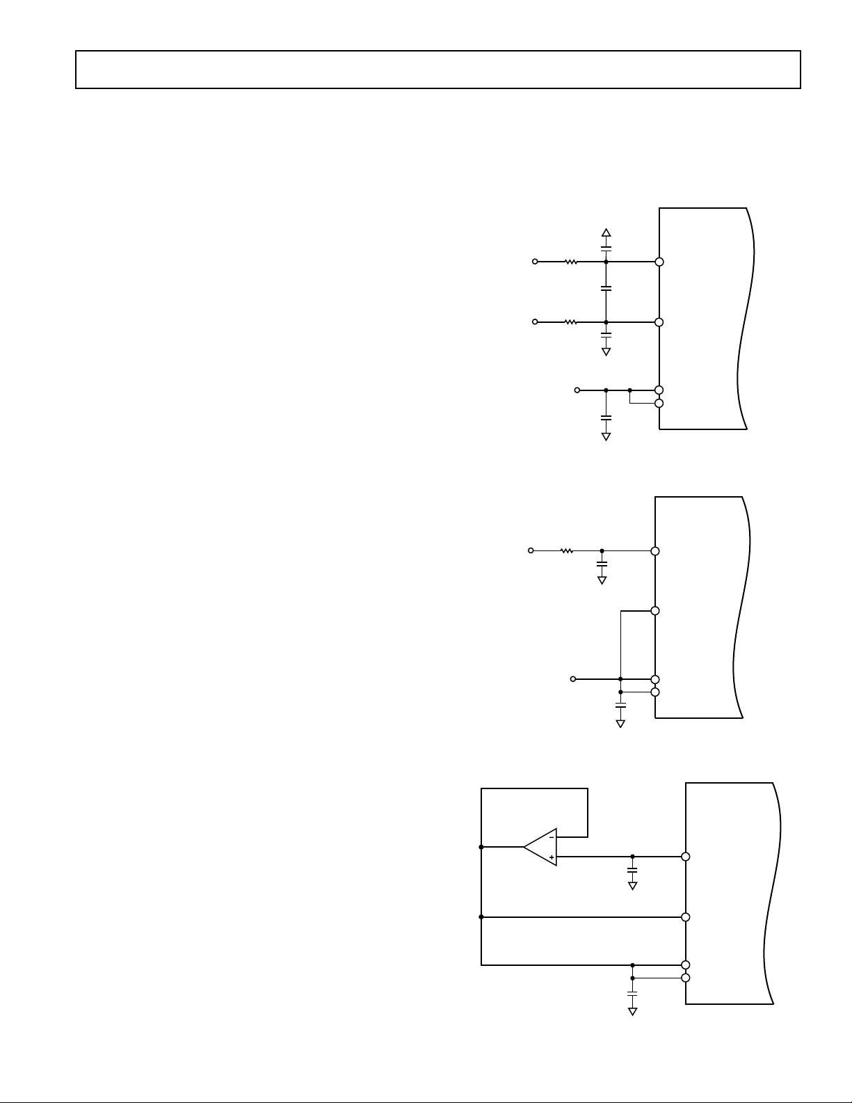
be configured as either a differential or single-ended input for
maximum flexibility in interfacing to external sensors and inputs.
The sigma-delta converter consists of two stages, a modulator
and a sinc filter, that combine to produce a 16-bit conversion.
For each channel, signal-to-noise ratios of 76 dB may be achieved,
corresponding to greater than 12 bits of resolution from each
as the RC filter shown in Figure 6, which provides a more than
30 dB attenuation to signals above 1 MHz (3 dB at 34 kHz) is adequate. The additional antialiasing band limiting required by the
Nyquist criterion for the 32.5 kHz sampling rate (a cutoff of
16.25 kHz) is supplied by the high order sinc filter in the digital
domain.
converter. Input signals up to 16.27 kHz may be converted.
For maximum flexibility, the five ADCs are arranged as two
ADMC300
banks; ADC1 and ADC2 forming Bank A, and ADC3, ADC4
and ADC5 forming Bank B. The characteristics of each bank,
such as sampling rate, internal or external conversion, synchronization to the PWM block, operating modes, may be controlled independently. The ADC registers of each bank may be
loaded from an internal signal whose frequency may be programmed as a precise fraction of the CLKIN frequency. Alternatively, the ADCs may be updated by an external signal on
VIN + V
–VIN + V
REF
REF
100
0.0047F
100
0.047F
Vx
VxN
0.047F
the CONVST pin. There are two dedicated ADC interrupts;
one for each bank of converters that can be used to signal that
the ADCs of the particular bank have been updated.
The ADC system also contains a built-in calibration function
that may be used to null any offsets within the ADC converters.
REF
0.1F
REFINA
REFINB
V
Each ADC channel may be placed in the calibration state individually or in combination with other channels.
In addition, the ADC system provides three multiplexer control
Figure 6. Differential Configuration for ADC Input of
ADMC300
pins that may be used in conjunction with an external multiplexer to permit external signal expansion.
ADMC300
There is a separate reference input for each bank of converters.
However, the ADMC300 also provides a reference output that
could be buffered and used as a reference source for either or
VIN + V
REF
100
0.047F
Vx
both banks.
Input Configuration
The input to each ADC may be applied to the ADMC300 in
VxN
either a single-ended or differential configuration. In many
cases, a single-ended configuration is easier to provide but the
differential connection permits the reduction of common-mode
noise from the input signal. Each ADC input may be configured for single-ended or differential inputs as appropriate,
completely independent of the other channels. Figure 6 illus-
V
REF
0.1F
REFINA
REFINB
trates a typical differential configuration for the inputs of one
ADC channel of the ADMC300. The input signals are applied
to pins Vx and VxN (for example V1 and V1N). For correct
operation and maximum input dynamic range, the inputs sig-
IN
REF
+ V
.
REF
,
nals should be centered on the reference voltage level, V
Therefore, the signal applied to the Vx pin should be V
where V
is the analog input voltage. The corresponding signal
IN
Figure 7. Single-Ended Configuration for ADC Input of
ADMC300
applied to the inverting terminal of the differential input, VxN,
+ V
is then –V
IN
ADC input is actually 2 V
The input RC combination of 100 Ω and 0.047 µF provides a
first-order low-pass antialiasing filter with a cutoff frequency of
so that the differential signal applied to the
REF
IN
.
34 kHz. An advantage to sigma-delta ADCs is that the initial
(analog) signal filtering required for antialiasing is much more
modest than that required by other ADCs. With the sigma-delta
ADC, the input filter needed for the analog signal only has to
cut off at one-half of the modulator frequency, rather than the
lower effective sampling frequency. For the ADMC300, the
modulator runs 64 times faster than the sampling frequency.
Thus for a 32.5 kHz sampling rate, the modulator frequency
is 2.08 MHz, meaning the needed cutoff for the analog input
signal is 1.04 MHz. Therefore, a simple first order filter, such
Figure 8. Connection of Internal Voltage Reference of
ADMC300
–13–REV. B
Page 14

ADMC300
The corresponding configuration for single-ended operation is
shown in Figure 7, where the inverting input is now tied directly to
+ V
the reference voltage level. The noninverting input is V
IN
REF
.
An antialiasing filter with a cutoff at 34 kHz is included on this
input. Clearly, the differential input voltage swing in this configuration is half that of the differential configuration. Therefore, when operating in single-ended mode, the input voltage,
, may be twice as large as that when operating differentially.
V
IN
To ensure correct operation, a 0.1 µF, high-quality capacitor
must be included at the reference input pins. A 0.1 µF capaci-
tor should also be used at the VREF pin, even if external references are used.
In both Figures 6 and 7, it is assumed that an external precision
reference is used to provide the reference voltage level, V
REF
.
For optimum operation, a high-performance 2.5 V reference
such as the AD580 is recommended. This reference is applied
directly to both input reference pins, REFINA and REFINB,
and is also applied to any external bias circuitry used to produce
the ADC input signals. For a lower cost solution, the ADMC300
also provides a reference output that may be used to provide the
signal. The reference output is available at the VREF pin.
V
REF
For correct operation, a 0.1 µF capacitor is required at this pin
even if the internal reference is not used. In addition, it is recommended that the V
signal be buffered in a unity-gain stage
REF
prior to use, as shown in Figure 8. Of course, since there are
two separate reference inputs, pins REFINA and REFINB, the
two banks of ADCs may be run differently, if required.
ADC Register Update
The sigma-delta converters of the ADMC300 operate at a
highly oversampled rate. A number of control bits in the
ADCCTRL register are used to control when and how data is
latched into the ADC data registers of each bank. The data
registers of each bank may be latched at a regular rate based on
either an internal or an external convert start signal. Bits 0–1 of
the ADCCTRL register determine whether the convert start
signal is internal or external. Bit 0 controls the operation of
Bank A and Bit 1 controls the operation of Bank B. If either of
these bits is set to 1, the data registers of the corresponding
ADC bank are latched within two CLKIN cycles of the occurrence of a rising edge on the CONVST pin (PIO9). Alternatively, if either bit is set to zero, internal mode is selected and
the ADCs of the particular bank are updated at a regular rate,
determined by the contents of the appropriate ADC sample
frequency division register, ADCDIVA or ADCDIVB.
Bits 2–3 of the ADCCTRL register can be used to place the
ADC banks in an alternative read mode. The read mode is
enabled by setting these bits to 1, effectively disabling the convert start mode. In the read mode, the ADC registers of the
particular bank are continuously updated at a rate equal to half
the DSP clock rate, so that data is effectively available on demand. Bit 2 of the ADCCTRL register is used to place ADC
Bank A in read mode, while Bit 3 is used for Bank B.
ADC Sample Rate Selection
Internal convert start mode is selected by clearing Bits 0 and 2
of the ADCCTRL register for Bank A and Bits 1 and 3 for Bank
B. In this mode, the ADC data registers are updated at a regular rate that is determined by the ADC clock divide registers,
ADCDIVA and ADCDIVB. Therefore, each bank can be configured for independent update rates by writing different values
to the two registers. When Bank A and Bank B are configured
for independent update rates, it is important that the REFINA
and REFINB pins are driven by separate voltage reference sources
to avoid excessive crosstalk between banks. The ADCDIVA and
ADCDIVB registers are 6-bit registers aligned in Bits 6–11 and
the value written to these registers is used to divide the CLKIN
frequency to provide the ADC update rate. A 12-bit value is
written to these registers, but since Bits 0–5 are ignored, the
value should be an integer multiple of 64 or 0x040. The resultant ADC update rates for Banks A and B may be expressed as:
f
f
S, A
CLKIN
=
ADCDIVA
f
CLKIN
=
ADCDIVB
where f
f
S, B
is the CLKIN frequency, equal to half the DSP
CLKIN
instruction rate. Therefore, writing a value of 0x180 (= 384)
gives an ADC update rate of 32.55 kHz with a CLKIN frequency
of 12.5 MHz. The maximum value that can be written to these
registers is 0xFC0, corresponding to an update rate of 3.1 kHz.
Since the maximum update rate is limited to 32.55 kHz, the permissible range of ADC divide values is 0x180 to 0xFC0 in steps
of 0x040.
Each ADC channel contains an input modulator that oversamples
the input signal at a high rate. The modulator sample frequency
is automatically set by the internal ADC control to be exactly
64 times the ADC update rate determined by the ADC divide
registers. This corresponds to an oversample ratio of 64. Therefore, in the case where ADCDIVA = 0x180, the input modulators
of ADC Bank A sample the input signal at 2.08 MHz and the
data registers ADC1 and ADC2 are updated at the 32.55 kHz
rate.
Synchronization of ADC and PWM Systems
In motor control applications, it is advantageous to synchronize
the operation of the ADC system to the PWM pulse generation.
The ADMC300 permits separate control of such synchronization for each ADC bank and permits sophisticated definition of
the particular way that the ADC and PWM systems are synchronized. Operation of Bank A of the ADC may be synchronized to
the PWM by setting Bit 7 of the ADCCTRL register. Similarly,
setting Bit 8 of the ADCCTRL register enables synchronization
of Bank B to the PWM.
At its simplest, the ADC and PWM systems may be programmed
to operate at the same frequency and be synchronized to one
another so that the ADC data registers are automatically updated
at the start of each PWM period. This mode of operation is
illustrated in Figure 9(a) and is enabled by writing identical
values to the PWM period register, PWMTM, and the ADC
divide register, ADCDIVA or ADCDIVB. Synchronization is
subsequently enabled by setting Bit 7 (for Bank A) or Bit 8 (for
Bank B) of the ADCCTRL register.
Additionally, a separate control register, ADCSYNC may be
used to phase shift the update of the ADC registers to some
suitably defined instant within the PWM period. In this mode,
the frequencies of the PWM and ADC register updating are still
the same but phase shifted relative to one another. This mode is
illustrated in Figure 9 (b). Again, the PWM period register and
ADC divide registers are loaded with the same value. However,
the offset of the ADC update within the PWM period is
programmed using the ADCSYNC register. The ADCSYNC
–14–
REV. B
Page 15

ADMC300
ANALOG
INPUT
3.5 V
V
REF
= 2.5 V
1.5V
0xAD30 0x0000 0x52D0
V1N
V1
ADC CODE
ANALOG
INPUT
4.5 V
V
REF
= 2.5 V
0.5V
0xAD30 0x0000 0x52D0
V1N
V1
ADC CODE
(a)
(b)
register is a 7-bit register so that the ADC sample period is
effectively subdivided into 128 equal time slices. The value
written to the ADCSYNC register is the number of such time
slices before the PWMSYNC pulse that the CONVST pulse is
active. In other words, the occurrence of the CONVST pulse
lags the PWMSYNC pulse of Figure 9 (b) by a time, T
OFFSET
,
that can be expressed as a fraction of the ADC update period:
T
OFFSET
(128 − ADCSYNC )
=
128
ADCDIVn
f
CLKIN
Therefore, for the case where ADCDIVA is 0x180 and ADCSYNC
is 0x060, the CONVST pulse will lag the PWMSYNC pulse by a
quarter of the ADC update period, or 7.68 µs, with a 12.5 MHz
CLKIN. The ability to phase shift the ADC update relative to
the PWMSYNC pulse is available only in single update mode of
the PWM.
It is also possible to operate the ADCs at a faster update rate
than the PWM switching frequency and still maintain synchronism, as illustrated in Figure 9 (c). In this example, the value
written to the ADCDIV registers is three times larger than the
value written to the PWMTM register, so that the ADC update
rate is three times faster than the PWM switching frequency.
Synchronism is maintained by setting Bits 7 and 8 of the
ADCCTRL register. In addition, it is possible to introduce a
phase shift between the ADC update and PWMSYNC pulses
while operating at different frequencies, as illustrated by Figure 9
(d). The offset is defined by the ADCSYNC register as a fraction
of the ADC update period in an identical manner to before.
ADC Transfer Characteristics
Each ADC converter of the ADMC300 consists of an input
modulator stage and a decimation filter stage that produces the
final conversion result. The output of the decimation filters are
16-bit, left-aligned, two’s complement representation of the
input signal, V
. The ideal ADC transfer characteristics for
IN
both single-ended and differential modes are shown in Figure
10. The transfer characteristics of the ADC when operated in
the differential configuration are shown in Figure 10 (a) and for
the single-ended configuration in Figure 10 (b). The peak-peak
input voltage is 4 V.
The output code of the ADCs is typically given by:
ADCx = 10,600 ×
V
2.5
Vx −VxN
()
REFIN
PWMSYNC
AH
CONVST
PWMSYNC
AH
CONVST
T
OFFSET
PWMSYNC
AH
CONVST
PWMTM/3
PWMSYNC
AH
CONVST
T
OFFSET
Figure 9. (a) Synchronization of ADC and PWM at Same
Frequency with No Offset, (b) Synchronization of ADC and
PWM at Same Frequency with Offset, (c) Synchronization
of ADC and PWM with No Offset and ADC Update at
Three Times the PWM Frequency (d) Synchronization of
ADC and PWM at Different Frequencies with Offset (PWM
Is Operating in Single Update Mode)
PWMTM/3
PWMTM
PWMCHA
PWMTM
PWMCHA
PWMTM
PWMCHA
PWMTM
PWMCHA
(a)
(b)
(c)
(d)
Figure 10. (a) Typical Transfer Characteristic of the ADC
in Differential Input Configuration (b) Typical Transfer
Characteristic of the ADC in Single-Ended
–15–REV. B
Page 16

ADMC300
ADC Group Delay
The digital filters of the ADCs carry out two important functions. First, they remove the out-of-band quantization noise,
which has been suitably shaped by the noise-shaping circuits of
the input modulator stages. The digital filters then decimate the
high frequency bitstream from the modulators to a lower rate
16-bit word. The lower rate is set by the ADC divide registers
for the respective ADC banks as described previously. The
antialiasing decimation filter may be modeled by the Z-domain
transfer function:
3
−64
1
H
(Z) =
SINC
1− z
64
1− z
−1
Associated with the sinc filters is a group delay that may be
approximated by:
1. 5
tφ=
f
S
where fS is the update rate of the particular ADC channel. In
order to minimize the impact of the group delay on the overall
performance of the control system, it is advantageous to oversample the ADCs at a rate faster than the PWM frequency.
ADC Calibration
The ADC system of the ADMC300 has a calibration feature
that may be used to null any offsets in the ADC channels. There
is a 5-bit ADC calibration register, ADCCAL that has a dedicated bit for each ADC channel. Setting the appropriate bit of
the ADCCAL register will place the respective ADC channel in
the offset calibration state. Bit 0 controls ADC1, Bit 1 controls ADC2, etc. When the appropriate bit of the ADCCAL
register is set, the two input pins associated with that ADC channel are effectively disconnected from the pins of the ADMC300
and connected internally to the reference voltage. After waiting for the settling time of the decimation filters, the resultant
ADC code is a measure of the offset for that particular ADC
channel. This number should be saved in memory and used to
correct all further measurements from that channel.
ADC Interrupt Generation
Two dedicated interrupts are associated with the ADC system
of the ADMC300, one for each of the ADC banks. The interrupts are generated after the ADC data registers of the particular bank have been updated by either an internal or external
CONVST pulse. Interrupts are not generated when the ADCs
are in the read mode. There are separate interrupt vector locations associated with each of the interrupt sources. The ADC
Bank A interrupt is the highest priority interrupt with its vector
address at program memory location 0x0030. The Bank B
interrupt is the third highest priority interrupt with a vector
address of 0x0038. Each interrupt has a four word space in the
vector table. The sequencing and masking of these interrupts is
managed by the Programmable Interrupt Controller (PIC)
block described later.
ADC Multiplexer Control
The ADMC300 has three digital output pins, MUX2, MUX1
and MUX0, that can be used to drive an external multiplexer to
feed additional analog inputs to the ADCs if required. Using
these control lines, up to eight analog signals could be externally multiplexed into each ADC channel, allowing expansion
up to 40 analog inputs. The state of the three multiplexer pins
is directly controlled from the ADCCTRL register, using Bits
4–6. Bit 4 of the ADCCTRL register directly controls the
MUX0 pin, so that setting this bit will place a HI level on the
MUX0 pin. Similarly, Bit 5 directly controls the MUX1 pin
and Bit 6 controls the MUX2 pin.
Because of the finite impulse response of the decimation filters
of the ADCs, it is usually only slower dynamic signals that are
multiplexed into the ADCs. In a typical motor control system,
such signals may comprise the dc link voltage, the output of
various temperature sensors, reference inputs, etc.
ADC Status
Because of the dynamic characteristics of the decimation filters
of the sigma-delta converters, it is necessary to allow the
impulse response of the filters to decay before meaningful,
accurate data is available. There is a one-bit status register,
ADCSTAT, in the ADMC300 that indicates whether or not
valid data is available from the ADC. Bit 0 of the ADCSTAT
register is asserted while the decimation filters are settling to
indicate that data is not yet valid. This BUSY bit can be programmed to represent the status of the decimation filters of either
Bank A or Bank B by programming Bit 9 of the ADCCTRL
register. The BUSY bit will go active for four ADC sample
periods any time that ADCCTRL, ADCCAL or ADCSYNC
are written to. If Bit 9 of the ADCCTRL register is cleared, the
BUSY bit will go active any time ADCDIVA is written to, and the
four ADC sample period width of the BUSY pulse will be four
ADC Bank A sample periods. If Bit 9 of the ADCCTRL register
is set, the BUSY bit will go active any time the ADCDIVB
register is written to, and the four ADC sample period width of
the BUSY pulse will be four ADC Bank B sample periods. It is
still possible to read the ADC data registers while the BUSY
signal is asserted. However, care must be taken in the interpretation of such data.
ADC Power-Down and Reset Features
The ADC section of the ADMC300 has certain power-down
features that may be used to reduce the overall power consumption of the part. Each bank of the ADC system may be individually
powered down if all channels of that bank are not used in a particular application. Setting Bit 10 of the ADCCTRL register will
power down the input modulators of both ADC channels of
ADC Bank A. Similarly, setting Bit 11 of the ADCCTRL
register will power down the three ADC channels of Bank B.
Clearing these bits will enable the input modulators of the
respective banks. On power-up, both Bits 10 and 11 of the
ADCCTRL register are set by default, so that all five input
modulator stages are disabled. To operate the required ADC
channels, the appropriate bits in the ADCCTRL register must
be cleared.
In addition, setting Bit 12 of the ADCCTRL register will
power down the internal reference circuitry. Further power
reduction is possible if this reference circuitry is powered down.
However, this bit has an effect only if both ADC banks are also
powered down. Clearing Bit 12 of the ADCCTRL register will
enable the internal reference circuitry.
It is also possible to force a reset of all five input modulators of
the ADC system by setting Bit 14 of the ADCCTRL register.
Setting Bit 15 of the ADCCTRL register will force a reset of
the decimation filters in all five ADC channels. In order to
come out of input modulator reset or decimation filter reset,
the respective bit must be cleared. On power-up, these bits are
–16–
REV. B
Page 17

ADMC300
cleared so that both the modulators and the decimation filters
come up in the normal mode. It is recommended that prior to
use, a full reset be performed.
ADC Registers
The composition of all the data registers associated with the ADC
system of the ADMC300 is shown at the end of the data sheet.
The reset values are shown for certain bits, where appropriate.
THREE-PHASE PWM CONTROLLER
The PWM generator block of the ADMC300 is a flexible,
programmable, three-phase PWM waveform generator that can
be programmed to generate the required switching patterns to
drive a three-phase voltage source inverter for ac induction
(ACIM) or permanent magnet synchronous (PMSM) motor
control. In addition, the PWM block contains special functions
that considerably simplify the generation of the required PWM
switching patterns for control of the electronically commutated
motor (ECM) or brushless dc motor (BDCM).
The PWM generator produces three pairs of PWM signals on
the six PWM output pins (AH, AL, BH, BL, CH and CL).
The six PWM output signals consist of three high side drive
signals (AH, BH and CH) and three low side drive signals (AL,
BL and CL). The polarity of the generated PWM signals may
be programmed by the PWMPOL pin, so that either active HI
or active LO PWM patterns can be produced by the ADMC300.
The switching frequency, dead time and minimum pulsewidths
of the generated PWM patterns are programmable using respectively the PWMTM, PWMDT and PWMPD registers. In
addition, three duty-cycle control registers (PWMCHA,
PWMCHB and PWMCHC) directly control the duty cycles of
the three pairs of PWM signals.
Each of the six PWM output signals can be enabled or disabled
by separate output enable bits of the PWMSEG register. In
addition, three control bits of the PWMSEG register permit
crossover of the two signals of a PWM pair for easy control of
ECM or BDCM. In crossover mode, the PWM signal destined
for the high side switch is diverted to the complementary lowside output and the signal destined for the low side switch is
diverted to the corresponding high side output signal.
In many applications, there is a need to provide an isolation
barrier in the gate-drive circuits that turn on the power devices
of the inverter. In general, there are two common isolation
techniques, optical isolation using opto-couplers and transformer isolation using pulse transformers. The PWM controller
of the ADMC300 permits mixing of the output PWM signals
with a high frequency chopping signal to permit easy interface
to such pulse transformers. The features of this gate-drive
chopping mode can be controlled by the PWMGATE register.
There is an 8-bit value within the PWMGATE register that
directly controls the chopping frequency. In addition, high
frequency chopping can be independently enabled for the high
side and the low side outputs using separate control bits in the
PWMGATE register.
The PWM generator is capable of operating in two distinct
modes, single update mode or double update mode. In single
update mode the duty cycle values are programmable only once
per PWM period, so that the resultant PWM patterns are symmetrical about the midpoint of the PWM period. In the double
update mode, a second updating of the PWM duty cycle values
is implemented at the midpoint of the PWM period. In this
mode, it is possible to produce asymmetrical PWM patterns,
that produce lower harmonic distortion in three-phase PWM
inverters. This technique also permits closed loop controllers to
change the average voltage applied to the machine windings at a
faster rate and so permits faster closed loop bandwidths to
be achieved. The operating mode of the PWM block (single
or double update mode) is selected by a control bit in the
MODECTRL register.
The PWM generator of the ADMC300 also provides an output
pulse on the PWMSYNC pin that is synchronized to the PWM
switching frequency. In single update mode a PWMSYNC pulse
is produced at the start of each PWM period. In double update
mode, an additional PWMSYNC pulse is produced at the midpoint of each PWM period. The width of the PWMSYNC pulse
is programmable through the PWMSYNCWT register.
The PWM signals produced by the ADMC300 can be shut off
in a number of different ways. First, there is a dedicated asynchronous PWM shutdown pin, PWMTRIP, that, when brought
LO, instantaneously places all six PWM outputs in the OFF
state (as determined by the state of the PWMPOL pin). In addition, each of the PIO lines of the ADMC300 (PIO0 to PIO11)
can be configured to act as an additional PWM shutdown. By
setting the appropriate bit in the PIOPWM register, the corresponding PIO line acts as an asynchronous PWM shutdown
source in a manner identical to the PWMTRIP pin. These two
hardware shutdown mechanisms are asynchronous so that the
associated PWM disable circuitry does not go through any
clocked logic, thereby ensuring correct PWM shutdown even in
the event of a loss of the DSP clock. In addition to the hardware
shutdown features, the PWM system may be shut down in software by writing to the PWMSWT register.
Status information about the PWM system of the ADMC300 is
available to the user in the SYSSTAT register. In particular, the
state of both the PWMTRIP and the PWMPOL pins is available, as well as a status bit that indicates whether operation is in
the first half or the second half of the PWM period.
A functional block diagram of the PWM controller is shown in
Figure 11. The generation of the six output PWM signals on
pins AH to CL is controlled by four important blocks:
• The Three-Phase PWM Timing Unit, which is the core of the
PWM controller, generates three pairs of complemented and
dead-time-adjusted center-based PWM signals.
• The Output Control Unit allows the redirection of the outputs
of the Three-Phase Timing Unit for each channel to either the
high side or the low side output. In addition, the Output Control Unit allows individual enabling/disabling of each of the six
PWM output signals.
• The Gate Drive Unit provides the correct polarity output
PWM signals based on the state of the PWMPOL pin. The
Gate Drive Unit also permits the generation of the high frequency chopping frequency and its subsequent mixing with
the PWM signals.
• The PWM Shutdown Controller takes care of the various
PWM shutdown modes (via the PWMTRIP pin, the PIO lines
or the PWMSWT register) and generates the correct RESET
signal for the Timing Unit.
–17–REV. B
Page 18

ADMC300
The PWM controller is driven by a clock at the same frequency
as the DSP instruction rate, CLKOUT, and is capable of generating two interrupts to the DSP core. One interrupt is generated
on the occurrence of a PWMSYNC pulse and the other is generated on the occurrence of any PWM shutdown action.
PWM
CONFIGURATION
REGISTERS
PWMTM (15…0)
PWMDT (9…0)
PWMPD(9…0)
PWMSYNCWT(7…0)
MODECTRL (6)
THREE-PHASE
PWM TIMING
CLK SYNC
PWMSYNC
TO INTERRUPT
CONTROLLER
PWMTRIP
PWM
DUTY CYCLE
REGISTERS
PWMCHA (15…0)
PWMCHB (15…0)
PWMCHC (15…0)
UNIT
RESET
PWMSEG
(8…0)
OUTPUT
CONTROL
UNIT
SYNC
OR
PWMSWT
(0)
PWM SHUTDOWN CONTROLLER
PWMGATE
(8…0)
GATE
DRIVE
UNIT
CLK POL
PIO
PWM
DETECT
PIOPWM
(11…0)
AH
AL
BH
BL
CH
CL
CLKOUT
PWMSYNC
PWMPOL
PWMTRIP
PIO0
:
:
PIO11
Figure 11. PWM Controller Overview
Three-Phase Timing Unit
The 16-bit three-phase timing unit is the core of the PWM
controller and produces three pairs of pulsewidth modulated
signals with high resolution and minimal processor overhead.
The outputs of this timing unit are active LO such that a low
level is interpreted as a command to turn ON the associated
power device. There are four main configuration registers
(PWMTM, PWMDT, PWMPD and PWMSYNCWT) that
determine the fundamental characteristics of the PWM outputs.
In addition, the operating mode of the PWM (single or double
update mode) is selected by Bit 6 of the MODECTRL register.
These registers, in conjunction with the three 16-bit duty cycle
registers (PWMCHA, PWMCHB and PWMCHC), control the
output of the three-phase timing unit.
PWM Switching Frequency, PWMTM Register
The PWM switching frequency is controlled by the PWM period register, PWMTM. The fundamental timing unit of
the PWM controller is t
CK
= 1/f
CLKOUT
where f
CLKOUT
is the
CLKOUT frequency (DSP instruction rate). Therefore, for a
25 MHz CLKOUT, the fundamental time increment is 40 ns.
The value written to the PWMTM register is effectively the
number of t
clock increments in half a PWM period. The
CK
required PWMTM value as a function of the desired PWM
switching frequency (f
PWMTM =
) and is given by:
PWM
f
CLKOUT
2 × f
PWM
f
CLKIN
=
f
PWM
Therefore, the PWM switching period, TS, can be written as:
T
= 2 × tCK × PWMTM
S
For example, for a 25 MHz CLKOUT and a desired PWM
switching frequency of 10 kHz (T
= 100 µs), the correct value
S
to load into the PWMTM register is:
6
PWMTM =
25 ×10
2 ×10 ×10
=1250
3
The largest value that can be written to the 16-bit PWMTM
register is 0xFFFF = 65,535, which corresponds to a minimum
PWM switching frequency of:
6
f
PWM, MIN
25 ×10
=
2 × 65,535
=190.74 Hz
for a CLKOUT frequency of 25 MHz.
PWM Switching Dead Time, PWMDT Register
The second important parameter that must be set up in the
initial configuration of the PWM block is the switching dead
time. This is a short delay time introduced between turning off
one PWM signal (say, AH) and turning on the complementary
signal, AL. This short time delay is introduced to permit the
power switch being turned off (in this case, AH) to completely
recover its blocking capability before the complementary switch
is turned on. This time delay prevents a potentially destructive
short-circuit condition from developing across the dc link
capacitor of a typical voltage source inverter.
The dead time is controlled by the 10-bit, read/write PWMDT
register. There is only one dead-time register that controls the
dead time inserted into all three pairs of PWM output signals.
The dead time, T
, is related to the value in the PWMDT regis-
D
ter by:
TD= PWMDT × 2 × tCK=
2 × PWMDT
f
CLKOUT
Therefore, a PWMDT value of 0x00A (= 10), introduces an
800 ns delay between the turn-off on any PWM signal (say, AH)
and the turn-on of its complementary signal (AL). The amount
of the dead time can therefore be programmed in increments of
(or 80 ns for a 25 MHz CLKOUT). The PWMDT register
2t
CK
is a 10-bit register so that its maximum value is 0x3FF (= 1023),
corresponding to a maximum programmed dead time of:
T
=1023 ×2 ×tCK=1023 ×2 ×40 ×10–9= 81.84 µs
D, MAX
for a CLKOUT rate of 25 MHz. Obviously, the dead time can
be programmed to be zero by writing 0 to the PWMDT register.
PWM Operating Mode, MODECTRL and SYSSTAT Registers
The PWM controller of the ADMC300 can operate in two
distinct modes; single update mode and double update mode.
The operating mode of the PWM controller is determined by
the state of Bit 6 of the MODECTRL register. If this bit is
cleared the PWM operates in the single update mode. Setting
Bit 6 places the PWM in the double update mode. By default,
following either a peripheral reset or power-on, Bit 6 of the
MODECTRL register is cleared so that the default operating
mode is single update mode.
–18–
REV. B
Page 19

ADMC300
In single update mode, a single PWMSYNC pulse is produced
in each PWM period. The rising edge of this signal marks the
start of a new PWM cycle and is used to latch new values from
the PWM configuration registers (PWMTM, PWMDT, PWMPD
and PWMSYNCWT) and the PWM duty cycle registers
(PWMCHA, PWMCHB and PWMCHC) into the three-phase
timing unit. In addition, the PWMSEG register is also latched
into the output control unit on the rising edge of the PWMSYNC pulse. In effect, this means that the characteristics and
resultant duty cycles of the PWM signals can be updated only
once per PWM period at the start of each cycle. The result is
that PWM patterns that are symmetrical about the midpoint of
the switching period are produced.
In double update mode, there is an additional PWMSYNC
pulse produced at the midpoint of each PWM period. The
rising edge of this new PWMSYNC pulse is again used to latch
new values of the PWM configuration registers, duty cycle
registers and the PWMSEG register. As a result it is possible to
alter both the characteristics (switching frequency, dead time,
minimum pulsewidth and PWMSYNC pulsewidth) as well as
the output duty cycles at the midpoint of each PWM cycle.
Consequently, it is possible to produce PWM switching patterns
that are no longer symmetrical about the midpoint of the period
(asymmetrical PWM patterns).
In double update mode, it may be necessary to know whether
operation at any point in time is in either the first half or the
second half of the PWM cycle. This information is provided by
Bit 3 of the SYSSTAT register, which is cleared during operation in the first half of each PWM period (between the rising
edge of the original PWMSYNC pulse and the rising edge of
the new PWMSYNC pulse introduced in double update mode).
Bit 3 of the SYSSTAT register is set during operation in the
second half of each PWM period. This status bit allows the user
to make a determination of the particular half-cycle during
implementation of the PWMSYNC interrupt service routine, if
required.
The advantage of double update mode is that lower harmonic
voltages can be produced by the PWM process and faster control bandwidths are possible. However, for a given PWM switching
frequency, the PWMSYNC pulses occur at twice the rate in the
double update mode. Since new duty cycle values must be
computed in each PWMSYNC interrupt service routine, there
is a larger computational burden on the DSP in double update
mode.
Width of the PWMSYNC Pulse, PWMSYNCWT Register
The PWM controller of the ADMC300 produces an output
PWM synchronization pulse at a rate equal to the PWM switching frequency in single update mode and at twice the PWM
frequency in the double update mode. This pulse is available
for external use at the PWMSYNC pin. The width of this
PWMSYNC pulse is programmable by the 8-bit read/write
PWMSYNCWT register. The width of the PWMSYNC pulse,
T
PWMSYNC
so that the width of the pulse is programmable from t
256t
, is given by:
T
PWMSYNC
(corresponding to 40 ns to 10.24 µs for a CLKOUT rate
CK
= tCK × (PWMSYNCWT + 1)
CK
to
of 25 MHz). Following a reset, the PWMSYNCWT register
contains 0x27 (= 39) so that the default PWMSYNC width is
1.6 µs.
PWM Duty Cycles, PWMCHA, PWMCHB, PWMCHC
Registers
The duty cycles of the six PWM output signals on pins AH to
CL are controlled by the three 16-bit read/write duty cycle
registers, PWMCHA, PWMCHB and PWMCHC. The integer
value in the register PWMCHA controls the duty cycle of the
signals on AH and AL, PWMCHB controls the duty cycle of
the signals on BH and BL and PWMCHC controls the duty
cycle of the signals on CH and CL. The duty cycle registers are
programmed in integer counts of the fundamental time unit,
, and define the desired on-time of the high-side PWM sig-
t
CK
nal produced by the three-phase timing unit over half the PWM
period. The switching signals produced by the three-phase
timing unit are also adjusted to incorporate the programmed
dead time value in the PWMDT register. The three-phase timing
unit produces active LO signals so that a LO level corresponds to a
command to turn on the associated power device.
A typical pair of PWM outputs (in this case for AH and AL)
from the timing unit are shown in Figure 12 for operation in
single update mode. All illustrated time values indicate the
integer value in the associated register and can be converted to
time by simply multiplying by the fundamental time increment,
t
. First, it is noted that the switching patterns are perfectly
CK
symmetrical about the midpoint of the switching period in this
single update mode since the same values of PWMCHA,
PWMTM and PWMDT are used to define the signals in both
half cycles of the period. It can be seen how the programmed
duty cycles are adjusted to incorporate the desired dead time
into the resultant pair of PWM signals. Clearly, the dead time is
incorporated by moving the switching instants of both PWM
signals (AH and AL) away from the instant set by the PWMCHA
register. Both switching edges are moved by an equal amount
(PWMDT × t
) to preserve the symmetrical output patterns.
CK
Also shown is the PWMSYNC pulse whose width is set by the
PWMSYNCWT register and Bit 3 of the SYSSTAT register
that indicates whether operation is in the first or second half
cycle of the PWM period.
PWMCHA PWMCHA
AH
2 PWMDT
AL
PWMSYNC
SYSSTAT (3)
PWMTM
2 PWMDT
PWMSYNCWT + 1
PWMTM
Figure 12. Typical PWM Outputs of Three-Phase Timing
Unit in Single Update Mode (Active LO Waveforms)
The resultant on-times of the PWM signals in Figure 12 may be
written as:
T
= 2 × (PWMCHA – PWMDT) × t
AH
TAL = 2 × (PWMTM – PWMCHA – PWMDT) × t
CK
CK
and the corresponding duty cycles are:
T
PWMCHA – PWMDT
dAH=
AH
=
T
S
PWMTM
–19–REV. B
Page 20

ADMC300
T
PWMTM – PWMCHA – PWMDT
dAL=
AL
=
T
S
PWMTM
The minimum permissible TAH and TAL values are zero, corresponding to a 0% duty cycle. In a similar fashion, the maximum
value is T
, corresponding to a 100% duty cycle.
S
The output signals from the timing unit for operation in double
update mode are shown in Figure 13. This illustrates a completely general case where the switching frequency, dead time
and duty cycle are all changed in the second half of the PWM
period. Of course, the same value for any or all of these quantities could be used in both halves of the PWM cycle. However, it
can be seen that there is no guarantee that symmetrical PWM
signals will be produced by the timing unit in double update
mode. Additionally, it is seen that the dead time is inserted into
the PWM signals in the same way as in the single update mode.
1
PWMCHA
2
2 PWMDT
PWMSYNCWT2 + 1
2
AH
AL
PWMSYNC
SYSSTAT (3)
2 PWMDT
PWMSYNCWT1 + 1
PWMCHA
1
have been written, internal counting of the timers in the
three-phase timing unit is enabled. Writing to the PWMTM
register starts the internal timing of the main PWM timer. Provided the PWMTM register is written prior to the PWMCHA,
PWMCHB and PWMCHC registers in the initialization,
the first PWMSYNC pulse and interrupt (if enabled) appear
1.5 × t
× PWMTM seconds after the initial write to the
CK
PWMTM register in single update mode. In double update
mode, the first PWMSYNC pulse appears after PWMTM ×
seconds.
t
CK
Effective PWM Resolution
In single update mode, the same value of PWMCHA, PWMCHB
and PWMCHC is used to define the on-times in both half
cycles of the PWM period. As a result the effective resolution
of the PWM generation process is 2t
(or 80 ns for a 25 MHz
CK
CLKOUT), since incrementing one of the duty cycle registers
by one changes the resultant on-time of the associated PWM
signals by t
in each half period (or 2tCK for the full period).
CK
In double update mode, improved resolution is possible since
different values of the duty cycle registers are used to define the
on-times in both the first and second halves of the PWM period. As a result, it is possible to adjust the on-time over the
whole period in increments of t
effective PWM resolution of t
. This corresponds to an
CK
in double update mode (or
CK
40 ns for a 25 MHz CLKOUT).
The achievable PWM switching frequency at a given PWM
resolution is tabulated in Table V.
PWMTM
1
PWMTM
2
Figure 13. Typical PWM Outputs of Three-Phase Timing
Unit in Double Update Mode (Active LO Waveforms)
In general the on-times of the PWM signals in double update
mode can be defined as:
TAH= (PWMCHA1+ PWMCHA2– PWMDT1– PWMDT2) × t
TAL= (PWMTM1+ PWMTM2– PWMCHA1– PWMCHA
–PWMDT1– PWMDT2) ×
t
CK
CK
2
where the subscript 1 refers to the value of that register during
the first half cycle and the subscript 2 refers to the value during
the second half cycle. The corresponding duty cycles are:
T
PWMCHA PWMCHA PWMDT PWMDT
( ––)
d
d
AH
==
AH
T
S
TTPWMTM PWMTM PWMCHA PWMCHA PWMDT PWMDT
( –– ––)
AL
==
AL
S
+
12 1 212
+
1212
PWMTM PWMTM
()
PWMTM PWMTM
()
+
12
+
12
since for the completely general case in double update mode, the
switching period is given by:
TS=(PWMTM1+ PWMTM2)×t
CK
Again, the values of TAH and TAL are constrained to lie between
zero and T
.
S
PWM signals similar to those illustrated in Figure 12 and Figure
13 can be produced on the BH, BL, CH and CL outputs by
programming the PWMCHB and PWMCHC registers in a
manner identical to that described for PWMCHA.
The PWM controller does not produce any PWM outputs until
all of the PWMTM, PWMCHA, PWMCHB and PWMCHC
registers have been written to at least once. Once these registers
–20–
Table V. Achievable PWM Resolution in Single and Double
Update Modes
Single Update Mode Double Update Mode
Resolution PWM Frequency PWM Frequency
(Bits) (kHz) (kHz)
8 48.8 97.6
9 24.4 48.8
10 12.2 24.4
11 6.1 12.2
12 3.05 6.1
Minimum Pulsewidth, PWMPD Register
In many power converter switching applications, it is desirable
to eliminate PWM switching signals below a certain width. It
takes a certain finite time to both turn on and turn off modern
power semiconductor devices. Therefore, if the width of any of
the PWM signals goes below some minimum value, it may be
desirable to completely eliminate the PWM switching for that
particular cycle.
The allowable minimum on-time for any of the six PWM outputs over half a PWM period that can be produced by the
PWM controller may be programmed using the PWMPD register. The minimum on-time is programmed in increments of t
CK
so that the minimum on-time that will be produced over any
half PWM period, T
, is related to the value in the PWMPD
MIN
register by:
T
= PWMPD × t
MIN
CK
so that a PWMPD value of 0x002 defines a permissible minimum on-time of 80 ns for a 25 MHz CLKOUT.
REV. B
Page 21

ADMC300
In each half cycle of the PWM, the timing unit checks the ontime of each of the six PWM signals. If any of the times is
found to be less than the value specified by the PWMPD register, the corresponding PWM signal is turned OFF for the entire
half period and its complementary signal is turned completely
ON.
Consider the example where PWMTM = 200, PWMCHA = 5,
PWMDT = 3, PWMPD = 10 with a CLKOUT of 25 MHz and
operation in single update mode. In this case, the PWM switching frequency is 62.5 kHz and the dead time is 240 ns. The
permissible on-time of any PWM signal over one-half of any
period is 400 ns. Clearly, for this example, the dead-time
adjusted on-time of the AH signal over half a PWM period is
(5–3) × 40 ns = 80 ns. This is less than the permissible value,
so the timing unit will output a completely OFF (0% duty
cycle) signal on AH. Additionally, the AL signal will be turned
ON for the entire half period (100% duty cycle).
Output Control Unit, PWMSEG Register
The operation of the Output Control Unit is controlled by the
9-bit read/write PWMSEG register. This register controls two
distinct features of the Output Control Unit that are directly
useful in the control of ECM or BDCM.
The PWMSEG register contains three crossover bits; one for
each pair of PWM outputs. Setting Bit 8 of the PWMSEG
register enables the crossover mode for the AH/AL pair of
PWM signals, setting Bit 7 enables crossover on the BH/BL
pair of PWM signals and setting Bit 6 enables crossover on the
CH/CL pair of PWM signals. If crossover mode is enabled for
any pair of PWM signals, the high-side PWM signal from the
timing unit (AH, for example) is diverted to the associated lowside output of the Output Control Unit so that the signal will
ultimately appear at the AL pin. Of course, the corresponding
low-side output of the Timing Unit is also diverted to the
complementary high-side output of the Output Control Unit so
that the signal appears at the AH pin. Following a reset, the
three crossover bits are cleared so that the crossover mode is
disabled on all three pairs of PWM signals.
The PWMSEG register also contains six bits (Bits 0 to 5) that
can be used to individually enable or disable each of the six
PWM outputs. The PWM signal of the AL pin is enabled by
setting Bit 5 of the PWMSEG register, while Bit 4 controls AH,
Bit 3 controls BL, Bit 2 controls BH, Bit 1 controls CL, and
Bit 0 controls the CH output. If the associated bit of the
PWMSEG register is set, the corresponding PWM output is
disabled irrespective of the value of the corresponding duty
cycle register. This PWM output signal will remain in the OFF
state as long as the corresponding enable/disable bit of the
PWMSEG register is set. The implementation of this output
enable function is implemented after the crossover function.
Following a reset, all six enable bits of the PWMSEG register
are cleared so that all PWM outputs are enabled by default.
In a manner identical to the duty cycle registers, the PWMSEG
is latched on the rising edge of the PWMSYNC signal so that
changes to this register only become effective at the start of
each PWM cycle in single update mode. In double update
mode, the PWMSEG register can also be updated at the midpoint of the PWM cycle.
In the control of an ECM only two inverter legs are switched at
any time and often the high-side device in one leg must be
switched ON at the same time as the low-side driver in a second
leg. Therefore, by programming identical duty cycles values for
two PWM channels (say PWMCHA = PWMCHB) and setting
Bit 7 of the PWMSEG register to cross over the BH/BL pair of
PWM signals, it is possible to turn ON the high-side switch of
Phase A and the low-side switch of Phase B at the same time.
In the control of ECM, it is usual that the third inverter leg
(Phase C in this example) be disabled for a number of PWM
cycles. This function is implemented by disabling both the CH
and CL PWM outputs by setting Bits 0 and 1 of the PWMSEG
register. This situation is illustrated in Figure 14, where it can
be seen that both the AH and BL signals are identical, since
PWMCHA = PWMCHB and the crossover bit for phase B is
set. In addition, the other four signals (AL, BH, CH and CL)
have been disabled by setting the appropriate enable/disable
bits of the PWMSEG register. For the situation illustrated in
Figure 14, the appropriate value for the PWMSEG register is
0x00A7. In normal ECM operation, each inverter leg is disabled for certain periods of time so that the PWMSEG register
is changed based on the position of the rotor shaft (motor commutation).
AH
BH
CH
AL
BL
CL
2
PWMDT
PWMTM
PWMCHA
= PWMCHB
PWMCHA
= PWMCHB
PWMTM
2
PWMDT
Figure 14. Example active LO PWM signals suitable for
ECM control, PWMCHA = PWMCHB, crossover BH/BL pair
and disable AL, BH, CH and CL outputs. Operation is in
single update mode.
Gate Drive Unit, PWMGATE Register
The Gate Drive Unit of the PWM controller adds features that
simplify the design of isolated gate drive circuits for PWM
inverters. If a transformer-coupled power device gate drive
amplifier is used then the active PWM signal must be chopped
at a high frequency. The 10-bit read/write PWMGATE register
allows the programming of this high frequency chopping mode.
The chopped active PWM signals may be required for the highside drivers only, for the low-side drivers only or for both the
high-side and low-side switches. Therefore, independent control of this mode for both high- and low-side switches is included
with two separate control bits in the PWMGATE register.
–21–REV. B
Page 22

ADMC300
Typical PWM output signals with high frequency chopping
enabled on both high-side and low-side signals are shown in
Figure 15. Chopping of the high side PWM outputs (AH, BH
and CH) is enabled by setting Bit 8 of the PWMGATE register. Chopping of the low-side PWM outputs (AL, BL and CL)
is enabled by setting Bit 9 of the PWMGATE register. The high
frequency chopping frequency is controlled by the 8-bit word
(GDCLK) placed in Bits 0 to 7 of the PWMGATE register.
The period of this high frequency carrier is:
T GDCLK t
=× +
CHOP CK
()
[]
×41
and the chopping frequency is therefore an integral subdivision
of the CLKOUT frequency:
f
CLKOUT
4 ×(GDCLK +1)
[]
f
CHOP
=
The GDCLK value may range from 0 to 255, corresponding
to a programmable chopping frequency rate from 24.4 kHz to
6.25 MHz for a 25 MHz CLKOUT rate. The gate drive features
must be programmed before operation of the PWM controller
and typically are not changed during normal operation of the
PWM controller. Following a reset, all bits of the PWMGATE
register are cleared so that high frequency chopping is disabled,
by default.
PWMCHA PWMCHA
AH
2
PWMDT
2
AL
[4
(GDCLK+1)
PWMTM
Figure 15. Typical Active LO PWM Signals with High Frequency Gate Chopping Enabled on Both High Side and
Low Side Switches (GDCLK is integer equivalent of value
in Bits 0 to 7 of PWMGATE register.)
PWM Polarity Control, PWMPOL Pin
tCK]
PWMTM
PWMDT
The polarity of the PWM signals produced at the output pins
AH to CL may be selected in hardware by the PWMPOL pin.
Connecting the PWMPOL pin to GND selects active LO PWM
outputs, such that a LO level is interpreted as a command to
turn on the associated power device. Conversely, connecting
VDD to the PWMPOL pin selects active HI PWM and the
associated power devices are turned ON by a HI level at the
PWM outputs. There is an internal pull-up on the PWMPOL
pin, so that if this pin becomes disconnected (or is not connected), active HI PWM will be produced. The level on the
PWMPOL pin may be read from Bit 2 of the SYSSTAT register, where a zero indicates a measured LO level at the PWMPOL
pin.
PWM Shutdown
In the event of external fault conditions, it is essential that
the PWM system be instantaneously shut down in a safe
fashion. A low level on the PWMTRIP pin provides an instantaneous, asynchronous (independent of the DSP clock)
shutdown of the PWM controller. All six PWM outputs are
placed in the OFF state (as defined by the PWMPOL pin).
In addition, the PWMSYNC pulse is disabled. The PWMTRIP
pin has an internal pull-down resistor so that if the pin becomes
disconnected the PWM will be disabled. The state of the
PWMTRIP pin can be read from Bit 0 of the SYSSTAT
register.
The 12 PIO lines of the ADMC300 can also be configured to
operate as PWM shutdown pins using the PIOPWM register.
The 12-bit PIOPWM has a control bit for each PIO line (Bit 0
controls PIO0 etc.). Setting the control bit enables the corresponding PIO line as a PWM shutdown pin. A low level on the
PIO line will then generate an instantaneous, asynchronous
shutdown of the PWM system, in a manner identical to the
PWMTRIP pin. On power-up, and following a reset, all PIO
lines are configured as inputs, have pull-downs and are programmed as PWM shutdown pins (PIOPWM = 0x0FFF) so
that the PWM is shut down. Correct operation of the PWM is
not possible without first correctly configuring the PIO system.
In addition, it is possible to initiate a PWM shutdown in software by writing to the 1-bit read/write PWMSWT register.
The act of writing to this register sets the bit in the PWMSWT
register and generates a PWM shutdown command in a manner
identical to the PWMTRIP or PIO pins. A hardware trip has no
effect on the PWMSWT register. Following a PWM shutdown, it
is possible to read the PWMSWT register to determine if the
shutdown was generated by hardware or software. Reading the
PWMSWT register automatically clears its contents.
On the occurrence of a PWM shutdown command (either from
the PWMTRIP pin, the PIO lines or the PWMSWT register), a
PWMTRIP interrupt will be generated. In addition, internal
timing of the three-phase timing unit of the PWM controller is
stopped. Following a PWM shutdown, the PWM can only be
re-enabled (in a PWMTRIP interrupt service routine, for example) by writing to all of the PWMTM, PWMCHA, PWMCHB
and PWMCHC registers. Provided the external fault has been
cleared and the PWMTRIP or appropriate PIO lines have returned to a HI level, internal timing of the three-phase timing
unit resumes and new duty-cycle values are latched on the next
PWMSYNC boundary.
PWM Registers
The configuration of all registers of the PWM system are shown
at the end of the data sheet.
ENCODER INTERFACE UNIT
The ADMC300 incorporates a powerful encoder interface block
to incremental shaft encoders, which are often used for position
feedback in high performance motion control systems. The encoder interface unit (EIU) includes a 16-bit quadrature up/down
counter and has three dedicated pins on the ADMC300. The
quadrature encoder signals are applied at the EIA and EIB pins
and the optional zero pulse may be applied at the EIZP pin. The
encoder interface unit will operate correctly with input frequencies up to slightly less than a quarter of the CLKIN frequency
(3.1 MHz for a 12.5 MHz CLKIN). The direction of counting
of the quadrature counter is programmable. In addition, the
actual direction of counting may be read from the EIU status
register, EIUSTAT.
The EIU may be programmed to use the zero pulse to reset the
quadrature encoder, if required. Alternatively, the zero pulse
can be ignored and the encoder quadrature counter is reset
according to the contents of a maximum count register,
–22–
REV. B
Page 23

ADMC300
EIUMAXCNT. There is also a single north marker mode available in which the encoder quadrature counter is reset only on
the first zero pulse. Both modes are enabled by dedicated control bits in the EIU control register, EIUCTRL. A status bit is
set in the EIUSTAT register on the first occurrence of the zero
pulse.
The Encoder Interface Unit can also be made to implement
some error checking functions. If the error checking mode is
enabled, upon the occurrence of a zero pulse, the contents of
the encoder counter register are compared with the expected
value (0 or EIUMAXCNT depending on the direction of rotation). If an encoder count error is detected (say due to a disconnected encoder line), a status bit in the EIUSTAT register is set
and an EIU interrupt is generated.
An additional status bit is provided in the EIUSTAT register,
which indicates the initialization state of the EIU. Until the
EIUMAXCNT register is written to, the EIU is not initialized.
Three status bits in the EIUSTAT register can also be read to
read the state of the three EIU pins, EIA, EIB and EIZP.
The Encoder Interface Unit of the ADMC300 contains a 16-bit
loop timer that behaves in a manner similar to the programmable interval timer of the DSP core. The loop timer consist of
a timer register, period register and scale register so that it can
be programmed to time-out and reload at appropriate intervals.
A control bit in the EIUCTRL register is used to enable/disable
this loop timer. When this loop timer times out, an EIU interrupt is generated. This interrupt could be used to control the
timing of speed and position control loops in high performance
drives.
The Encoder Interface Unit also includes a high performance
Encoder Event Timer (EET) block that permits the accurate
timing of successive events of the encoder inputs. The EET can
be programmed to time the duration between up to 256 encoder
pulses and can be used to enhance velocity estimation, particularly at low speeds of rotation. The information from the registers of the EET block can be latched in two ways. In one mode,
both the contents of the EIU quadrature count register, EIUCNT
and all relevant EET registers (EETT and EETDELTAT) are
latched when the EIU loop timer times out. In the second
mode, the act of reading the EIUCNT register also simultaneously latches the EET registers. The EET data latching mode
is selected by a control bit in the EIUCTRL register.
Encoder Loop Timer
The EIU contains a 16-bit loop timer that is structured in a
manner similar to the interval timer of the DSP core (TCOUNT,
TPERIOD and TSCALE registers). The corresponding registers of the encoder loop timer are EIUTIMER, EIUPERIOD
and EIUSCALE. The EIU loop timer is clocked at the CLKIN
rate.
The EIU loop timer can be used to generate periodic interrupts
based on multiples of the CLKIN cycle times. The EIU loop
timer is enabled by setting Bit 5 of the EIUCTRL register.
When enabled, the 16-bit timer register (EIUTIMER) is decremented every N cycles, where N-1 is the scaling value stored in
the 8-bit EIUSCALE register. When the value of the EIUTIMER
register reaches zero an EIU interrupt is generated and the
EIUTIMER register is reloaded with the 16-bit value in the
EIUPERIOD register.
The scaling feature of this timer, provided by the EIUSCALE
register, allows the 16-bit timer to generate periodic interrupts
over a wide range of periods. For a 12.5 MHz CLKIN rate
(80 ns period), the timer can generate interrupts with periods of
80 ns up to 5.24 ms with a zero scale value (EIUSCALE = 0).
When scaling is used, time periods can range up to 1.34 seconds.
The EIU interrupt can be masked in the PICMASK register.
Encoder Interface Structure and Operation
The functional block diagram of the entire encoder interface
system of the ADMC300 is shown in Figure 16. The encoder
interface section consists of a 16-bit quadrature up/down counter,
a 16-bit read/write EIUCNT register that allows the up/down
counter to be read by the DSP. There is also a 16-bit read/
write EIUMAXCNT register that must be written to initialize
the encoder system. Until the EIUMAXCNT register has been
written to, the Encoder Interface Unit is not initialized and Bit 2
of the EIUSTAT register is set. The contents of the EIUMAXCNT
register are used in certain operating modes to reset the quadrature counter. The contents of the EIUMAXCNT register are
also used for error checking of the EIU. Operation of the encoder interface is controlled by the 6-bit read/write EIUCTRL
register.
Typical encoder waveforms are illustrated in Figure 17. The
contents of the quadrature counter are updated on each edge of
both encoder signals applied on the EIA and EIB pins. Prior to
application to the quadrature counter, these signals are synchronized to the CLKIN rate in input synchronization buffers. This
eliminates the asynchronous nature of real world encoder signals
prior to use in the Encoder Interface Unit logic.
Encoder Counter Direction
The direction of quadrature counting is determined by the REV
bit (Bit 0) of the EIUCTRL register. If the REV bit is cleared,
the signal at the EIA pin is fed to the A input of the quadrature
counter, and the EIB pin is fed to the B input. Thus, if the EIAencoder signal leads the EIB signal (and therefore the A signal
leads the B signal), the quadrature counter is incremented on
each edge, as shown in Figure 17. This (A signal leads the B
signal) is defined as the forward direction of motion. Setting
Bit 0 of the EIUCTRL register causes the signal at the EIA pin
to be fed to the B input of the quadrature counter and the signal
EIB becomes the A input of the quadrature counter. Therefore,
if the EIA signal leads the EIB signal at the pins of the ADMC300,
the A input to the quadrature counter will now lag the B input.
This will be recognized as rotation in the reverse direction and
the counter will be decremented on each quadrature pulse.
Following a reset, the REV bit is cleared.
As shown in Figure 16, the two encoder signals are used to
derive a quadrature signal that is used, in conjunction with a
direction bit, to increment or decrement the encoder counter
and also the Encoder Event Timer. The status of the direction
signal is indicated at Bit 1 of the EIUSTAT register. While the
encoder counter is incrementing, Bit 1 is set. Alternatively,
when the encoder counter is decrementing, Bit 1 of the EIUSTAT
register is cleared.
–23–REV. B
Page 24

ADMC300
Encoder Counter Reset
The ZERO bit (Bit 1) of the EIUCTRL register determines if
the encoder zero marker is used to reset the up/down counter of
the encoder interface. When Bit 1 of the EIUCTRL register is
set, the zero marker signal is used to reset the up/down counter
to zero (if moving in the forward direction) or to the value in
the EIUMAXCNT register (if moving in the reverse direction).
The reset operation takes place on the next quadrature pulse
after the zero marker has been recognized. In order to ensure
correct encoder counting (no missing or spurious codes) the
logic in the encoder counter latches the conditions (appropriate
encoder edge) at which the first reset is performed. Thereafter,
irrespective of operating conditions, the encoder reset operation
is always aligned with the same encoder edge. For example, if
the first reset operation occurs on the rising edge of B and the
encoder is moving in the forward direction, then all subsequent
reset operations are aligned with the rising edge of the B signal
(while moving in the forward direction) and on the falling edge
of B for rotation in the reverse direction. In order to account for
zero marker signals of different widths, the zero marker will be
recognized as the rising edge of the EIZP signal when moving in
the forward direction. When moving in the reverse direction, the
zero marker is recognized at the falling edge of the signal at the
EIZP pin.
When the ZERO bit of the EIUCTRL register is cleared, the
zero marker is not used at all by the encoder interface circuitry.
In this mode, the contents of the EIUMAXCNT register are
used as the reset value for the up/down counter. For example,
for an N-line incremental encoder, the appropriate value to
write to the EIUMAXCNT register is 4N-1. Therefore, for a
1024 line encoder, a value of 0x0FFF (= 4095) would be written to the EIUMAXCNT register. However, since absolute
position information is not available in this mode, due to the
absence of the zero marker, the full 16-bit range of the quadrature counter may be employed by writing a value of 0xFFFF to
the EIUMAXCNT register. Following a reset, the ZERO bit is
cleared.
The value written to the EIUMAXCNT register must be in the
form 4N-1, where N is any integer.
Single North Marker Mode
A further reset mode is available in the Encoder Interface Unit
called Single North Marker Mode. This mode is enabled by set-
ting Bit 2 (SNM) of the EIUCTRL register. For this mode to
operate, the ZERO bit (Bit 1) of the EIUCTRL register must
also be set. In this mode the EIUCNT register is reset (to zero
or EIUMAXCNT depending on direction) only on the first
occurrence of the zero marker. Subsequently, the EIUCNT register is reset by the natural roll-over to zero or the value in the
EIUMAXCNT register. Following a reset, this SNM bit is
cleared.
Bit 6 of the EIUSTAT register is used to signal the first occurrence of a zero marker. When the first zero marker has been
recognized by the EIU, Bit 6 of the EIUSTAT register is set.
Encoder Error Checking
Error checking in the EIU is enabled by setting Bit 3 (MON) of
the EIUCTRL register. The ZERO bit of the EIUCTRL register must also be set for error checking to be enabled. In this mode,
the contents of the EIUCNT register are compared with the
expected value (zero or EIUMAXCNT depending on direction)
when the zero marker is detected. If a value other than the expected value is detected, an error condition is generated by
setting Bit 0 of the EIUSTAT register and triggering an EIU
interrupt. Since the EIU interrupt can be initiated by both this
error checking function and the time-out of the encoder loop
timer, this status bit must be read to determine the source of the
interrupt if both are possible. Obviously if the encoder loop
timer is disabled, the EIU interrupt can only be generated by
this error-checking function. This EIU interrupt is also managed
and may be masked by the programmable interrupt controller
(PIC) block. The encoder continues to count encoder edges
after an error has been detected. Bit 0 of the EIUSTAT register
is cleared on the occurrence of the next zero marker provided
the error condition no longer exists and the EIUCNT register
again matches the expected value. Following a reset, the MON
bit is cleared.
Encoder Pin Status
Three additional status bits are provided in the EIUSTAT register that provide a measure of the state of the three EIU pins
(EIA, EIB and EIZP) following the synchronization buffers.
Bit 3 indicates the state of the EIA pin, Bit 4 indicates the state
of the EIB pin and Bit 5 gives the state of the EIZP pin. The
value of these status bits read is not affected by any of the control bits in the EIUCTRL register.
ENCODER EVENT TIMER BLOCK
CLKIN
EIUSCALE (7…0)
EIUTIMER (15…0)
EIUPERIOD (15…0)
ENCODER
LOOP
TIMER
EIA
SYNCHRONIZA-
EIB
EIZP
BUFFERS
EIUSTAT(5…3)
ENCODER
INTERFACE
BLOCK
TION
TIMEOUT
DIRECTION
A
B
ZP
MON
CLOCK DIVIDER
CLK
ENCODER EVENT
TIMER
PULSE
DECIMATOR
16-BIT
QUADRATURE
UP/DOWN
COUNTER
ENCODER
COUNTER
ERROR
CHECKING
ZERO
REV
SNM
EIUCTRL(5…0)
EETDIV(15…0)
EETSTAT(0)
EETT(15…0)
EETDELTAT(15…0)
EETN(7…0)
QUADRATURE SIGNAL
EETCNT(15…0)
EIUCNT(15…0)
EIUMAXCNT(15…0)
EIUSTAT(2…0)
INTERRUPT
OR
DSP DATA
MEMORY BUS
EIU
Figure 16. Configuration of Encoder Interface System of
ADMC300
–24–
REV. B
Page 25

ADMC300
EIA
QUADRATURE
ENCODER EVENT
TIMER VALUE
EIB
SIGNAL
EIUCNT
VELOCITY
EVENTS
EIUCNT
READ
EETDELTAT
EETT
Figure 17. Operation of Encoder Interface Unit and Encoder Event Timer of ADMC300 in forward direction with
EETN = 2.
Encoder Event Timer
The Encoder Event Timer block forms an integral part of the
EIU of the ADMC300. The EET accurately times the duration
between encoder events. The information provided by the EET
may be used to make allowances for the asynchronous timing of
encoder and DSP-reading events. As a result, more accurate
computations of the position and velocity of the motor shaft
may be performed.
The EET consists of a 16-bit encoder event timer, an encoder
pulse decimator and a clock divider as shown in Figure 16. The
EET clock frequency is selected by the 16-bit read/write
EETDIV clock divide register, whose value divides the CLKIN
frequency. The contents of the encoder event timer are incremented on each rising edge of the divided clock signal. An
EETDIV value of zero gives the maximum divide value of
0x10000 (= 65,536), so that the clock frequency to the encoder
event timer is at its minimum possible value.
The quadrature signal from the Encoder Interface Unit is decimated at a rate determined by the 8-bit read/write EETN register. For example, writing a value of 2 to EETN, produces a
pulse decimator output train at half the quadrature signal frequency, as shown in Figure 17. The rising edge of this decimated signal is termed a velocity event. Therefore, for an
EETN value of 2, a velocity event occurs every two encoder
edges, or on each edge of one of the encoder signals. An EETN
value of zero gives an effective pulse decimation value of 256.
On the occurrence of a velocity event, the contents of the encoder event timer are stored in an intermediate Interval Time
register. Under normal operation, this register stores the
elapsed time between successive velocity events. After, the
timer value has been latched at the velocity event, the contents
of the encoder event timer are reset to one.
Latching Data from the EET
When using the data from the Encoder Event Timer, it is important to latch a triplet set of data at the same instant in time.
The three pieces of data are the contents of the encoder
quadrature up/down counter, the stored value in the Interval
Time register (giving the precise measured time between the
last two velocity events) and the present value of the encoder
event timer (giving an indication of how much time has passed
since the last velocity event).
The data from the EET can be latched on the occurrence
of either of two different events. The particular event is
selected by Bit 4 (EETLATCH) of the EIUCTRL register.
Setting this EETLATCH bit causes the data to be latched on
the time-out of the encoder loop timer (EIUTIMER). At that
time, the contents of the encoder quadrature counter (EIUCNT)
are latched to a 16-bit, read-only register EETCNT. In addition, the contents of the intermediate Interval Time register are
latched to the EETT register and the contents of the encoder
event timer are latched to the EETDELTAT register. The
three registers, EETCNT, EETT and EETDELTAT then
contain the desired triplet of position/time data required for
the control algorithm. In addition, if the time-out of the
EIUTIMER is used to generate an interrupt, the required data
is automatically latched and waiting for execution of the interrupt service routine (which may be some time after the time-out
instant if there are multiple interrupts in the system). By latching the EIUCNT register to the EETCNT, the user does not
have to worry about changes in the EIUCNT register (due
to additional encoder edges) prior to servicing of the EIU
interrupt.
The other EET latch event is chosen by clearing the EETLATCH
bit of the EIUCTRL register. In this mode, whenever the
EIUCNT register is read by the DSP, the current value of the
intermediate Interval Time register is latched to the EETT
register and the current value of the encoder event timer is
latched to the EETDELTAT register. The three registers,
EIUCNT, EETT and EETDELTAT now contain the desired
triplet of position/speed data required for the control algorithm.
Note the difference from before in that the encoder count value
is now available in the EIUCNT register.
It is important to realize that the EETT and EETDELTAT registers are only updated by either the time-out of the EIUTIMER
register (if EETLATCH bit is set) or the act of reading the
EIUCNT register (if the EETLATCH bit is cleared). Therefore,
if the EETLATCH bit is set, the act of reading the EIUCNT
register will not update the EETT and EETDELTAT registers.
Following a reset, Bit 4 of the EIUCTRL is cleared.
EET Status Register
There is a 1-bit EETSTAT register that indicates whether or
not an overflow of the EET has occurred. If the time between
successive velocity events is sufficiently long, it is possible that
the encoder event timer will overflow. When this condition is
detected, Bit 0 of the EETSTAT register is set and the EETT
register is fixed at 0xFFFF. Reading the EETSTAT register
clears the overflow bit and permits the EETT register to be updated at the next velocity event. If an encoder direction reversal
is detected by the EIU, the encoder event timer is set to zero
and the EETT register is set to its maximum 0xFFFF value.
Subsequent velocity events will cause the EETT register to be
updated with the correct value. If a value of 0xFFFF is read from
the EETT register, Bit 0 of the EETSTAT register can be read
to determine whether an overflow or direction reversal condition exists. In the case of a direction reversal, the contents of the
EETDELTAT register is valid, representing
the time from the direction reversal to the instant at which the
EIUCNT register is read. On reset the EETN, EETDIV,
EETDELTAT and EETT registers are all cleared to zero.
Whenever either the EETN or EETDIV registers are written to,
the encoder event timer is reset to zero and the EETT register is
set to zero.
–25–REV. B
Page 26

ADMC300
EIU/EET Registers
The EIU and EET registers are summarized at the end of the
data sheet.
PROGRAMMABLE INPUT/OUTPUT
The ADMC300 has 12 programmable digital input/output pins
called PIO0 to PIO11. Each pin may be individually configured
as either an input or an output. An associated data register may
be used to read data from pins configured as inputs and write
data to pins configured as outputs. In addition, each I/O line
may be configured as an interrupt source. Both edge (rising and
falling) and level (high and low) interrupts may be detected.
Four of the PIO lines (PIO0 to PIO3) have dedicated vector
addresses in the interrupt table. The remaining eight interrupts
(PIO4 to PIO11) are multiplexed into a single additional interrupt vector location. The PIOFLAG register is used to determine which line caused the interrupt.
In addition, all PIO lines may be alternatively configured as
PWM trip sources. The PIOPWM register has dedicated bits
that may be used to enable this function on each PIO line. In
this mode, a low level on any pin configured as a PWM trip source
shuts down the PWM in a manner identical to the PWMTRIP pin.
PIO Configuration
Each of the 12 programmable input/output lines may be configured as either an input or an output by programming the appropriate bits of the PIODIR register. This 12-bit read/write register
has one bit associated with each I/O line; Bit 0 corresponds to
PIO0, etc. Clearing a bit in the PIODIR register will configure
the corresponding pin as an input pin. Conversely, setting a bit
configures the pin as an output pin. On reset, bits of the PIODIR
register are cleared so that all 12 PIO pins are configured as
inputs. In addition, all PIO lines are internally pulled down in
the ADMC300 so that unconnected lines are seen as low level
inputs.
Three of the PIO lines also serve alternate functions. PIO9 is
multiplexed as the external convert start signal for the ADC
system. Signals on this pin can be used to trigger updating of
the ADC data registers, if required. Also, PIO10 and PIO11
may be used as inputs to the Event Timer Unit (ETU) to accurately time the period, frequency or duty cycle of external signals. If these functions are not required, the three pins may be
used as general purpose I/O lines.
PIO Data Reading/Writing
Associated with the PIO system is a data register, PIODATA,
that also has a bit associated with each I/O line. Data written to
the PIODATA register will appear on those pins configured as
outputs. In addition, reading the PIODATA register will read
the data from those pins configured as inputs.
PIO Interrupt Generation
Each of the twelve PIO lines may be configured as an interrupt
source. Four of the PIO lines, PIO0 to PIO3, have dedicated
interrupt vector locations while the remaining eight are multiplexed into an additional interrupt vector. The PIOINTEN
enable function is used to enable or disable interrupts on the
PIO4 to PIO11 lines. The PICMASK register of the programmable interrupt controller is used to enable interrupts on the
four dedicated PIO lines, PIO0 to PIO3. Interrupts may be
generated on either edge (rising or falling) or level (high or
low) events by programming the appropriate bits of both the
PIOMODE and PIOLEVEL registers. Both registers have a
dedicated bit for each of the twelve PIO lines. Setting the appropriate bit of the PIOMODE register configures the interrupt as
level-sensitive, while clearing the bit configures the corresponding PIO to be edge sensitive. In level-sensitive mode
(PIOMODE bit is 1), setting the corresponding bit in the
PIOLEVEL register configures the interrupt as active high,
while clearing the bit in the PIOLEVEL register configures it for
active low. In edge-sensitive mode (PIOMODE bit is 0), setting
the corresponding bit of the PIOLEVEL register configures the
interrupt for rising edge, while clearing the bit configures the
interrupt for falling edge. On reset, all PIO interrupts are disabled. The appropriate register settings for correct PIO interrupt configuration is shown in Table VI.
Table VI. PIO Interrupt Configuration
PIOMODE
PIOLEVEL 0 1
0 Falling Edge Active Low
1 Rising Edge Active High
The four dedicated PIO interrupts from PIO0 to PIO3 have
interrupt vector addresses at program memory addresses 0x0048
for PIO0, 0x004C for PIO1, 0x0050 for PIO2 and 0x0054 for
PIO3. In the event of an interrupt on PIO4 to PIO11, the corresponding bit of the PIOFLAG register is set and the general
PIO interrupt is activated. This interrupt has a dedicated vector
address at location 0x003C. In the interrupt service routine for
this interrupt, the user must poll the PIOFLAG register to determine which of the PIO4 to PIO11 lines, that have interrupts
enabled, caused the interrupt. Of course, if only one of the PIO4 to
PIO11 lines have interrupts enabled, no polling is necessary.
Reading the PIOFLAG register clears all bits of the register.
PIO lines that are configured as outputs may also be used to
generate interrupts. If, for example, one of the PIO lines is
configured simultaneously as an output and as an interrupt
source, writing the appropriate data to the PIODATA register
will trigger an interrupt.
PIO as PWM Trip Sources
By setting the appropriate bits of the PIOPWM register, each of
the twelve PIO lines can be configured as a PWM trip source.
In this mode, a low level on the PIO pin will cause a PWM trip
that will disable all six PWM outputs on AH to CL. The disabling of the PWM is independent of the DSP clock, so that the
PWM stage can be fully protected even in the event of a loss of
clock signal to the DSP.
A PWMTRIP interrupt will be generated when the PWM is
reset (whether the PWM is reset via a PIO configured as a trip
source, or via the PWMTRIP pin). It is also possible to generate
the normal PIO interrupts on the occurrence of a falling-edge
on the PIO line. The advantage of this highly flexible structure
for PWM shutdown is that multiple fault signals could be applied to the ADMC300 at different PIO lines. The occurrence
of a falling-edge on any of them will instantaneously shut down
the PWM. However, based on the particular PIO interrupt that
is flagged, the user can easily determine the source of the trip.
This permits the action of the interrupt service routines following a PWM trip to be tailored to the particular fault that occurred.
On reset, all PIO lines are configured as PWM trip sources.
Because all PIO lines are also configured as inputs and have
–26–
REV. B
Page 27

ADMC300
internal pull-down resistors, any unconnected PIO lines will
cause a PWM trip. Therefore, prior to using the PWM unit of
the ADMC300, it is imperative that the PIO state be correctly
configured for the particular application.
PIO Registers
The configuration of all registers associated with the PIO system are shown at the end of the data sheet. Each of the registers
has a bit directly associated with one of the PIO lines. For example, Bit 0 of all registers affects only the PIO0 line of the
ADMC300.
AUXILIARY PWM OUTPUTS
The ADMC300 provides two auxiliary, fixed-frequency, variable duty cycle PWM outputs that may be used to drive auxiliary switching circuits in the motor control system. Alternatively,
by adding appropriate filtering at the output, these signals can
be used to provide a simple digital-to-analog converter. These
output signals appear on the AUX0 and AUX1 pins and are controlled by the duty cycle registers, AUXTIM0 and AUXTIM1.
The auxiliary PWM outputs operate at a fixed frequency that is
f
/256. This gives an auxiliary PWM switching frequency of
CLKIN
48.8 kHz for a 12.5 MHz CLKIN. The output duty cycle at the
auxiliary PWM output pin is controlled by comparing the 8-bit
auxiliary PWM duty-cycle registers, AUXTIM0 and AUXTIM1
with the contents of a timer. The value written to these registers
may range from 0 to 255 so that duty cycles from 0 to 99.6%
may be produced at the output pins. A simple filter at the
output could then be used to produce a corresponding analog
output from 0 to 0.996 V
DD
.
The outputs of the two auxiliary PWM timer circuits are synchronized on their rising edges. When the auxiliary timer registers are
written to, the value becomes effective immediately. Therefore,
if the value is smaller than the present timer value, the outputs
go low immediately. The correct duty cycle appears for the
subsequent auxiliary PWM period. On reset, the AUXTIM0
and AUXTIM1 registers are cleared so that no auxiliary PWM
signals are produced and the AUX0 and AUX1 pins are low
until these registers are programmed. The format of the
AUXTIM0 and AUXTIM1 registers is shown at the end of the
data sheet.
WATCHDOG TIMER
The ADMC300 incorporates a watchdog timer that can perform a full reset of the DSP and motor control peripherals in
the event of software error. The watchdog timer is enabled by
writing a timeout value to the 16-bit WDTIMER register. The
timeout value represents the number of CLKIN cycles required
for the watchdog timer to count down to zero. When the
watchdog timer reaches zero, a full DSP core and motor control
peripheral reset is performed. In addition, Bit 1 of the SYSSTAT
register is set so that after reset the ADMC300 can determine
that the reset was due to the time out of the watchdog timer and
not a power-on reset. Following a reset, Bit 1 of the SYSSTAT
register may be cleared by writing zero to the WDTIMER register. This clears the status bit but does not enable the watchdog
timer.
On reset, the watchdog timer is disabled and is only enabled
when the first timeout value is written to the WDTIMER
register. To prevent the watchdog timer from timing out, the
user must write to the WDTIMER register at regular intervals
(shorter than the programmed WDTIMER period value). On all
but the first write to WDTIMER, the particular value written to
the register is unimportant since writing to WDTIMER simply
reloads the first value written to this register.
EVENT TIMER UNIT
The ADMC300 contains a dual channel Event Timer Unit
(ETU) that may be used to accurately measure the elapsed time
between defined events on a particular channel. The ETU uses
two input pins, ETU0 and ETU1, that are multiplexed with the
PIO10 and PIO11 pins. The ETU system contains a set of
16-bit data registers that are used to store the value of the
dedicated ETU timer on the occurrence of the defined events
on the input pins. A configuration register is used to define the
nature of the events on each of the input pins. In addition, a
control register is used to initiate event capture on the inputs. A
status register may be read to determine the state of the two
capture channels. A dedicated ETU interrupt may be generated
upon completion of a capture sequence on either the ETU0 or
ETU1 channel.
The ETU timer is a free running counter whose contents may be
read from the 16-bit ETUTIME read only register.
An event may be defined as either a rising or falling edge on the
associated ETU0 and ETU1 inputs pins. Therefore, the ETU
system can be used to compute the frequency, period, duty
cycle or on-time of signals applied at the inputs. A functional
block diagram of the ETU system of the ADMC300 is shown
in Figure 18.
ETU Event Definition
The ETU system of the ADMC300 contains a dedicated 16-bit
timer whose clock frequency may be programmed using the
ETUDIVIDE register. This register divides the CLKIN frequency
to provide the clock signal for the ETU timer. The clock
frequency of the ETU timer may be expressed as f
CLKIN
/
ETUDIVIDE and is common to both channels.
Two events are used to trigger the ETU, termed Event A and
Event B. By setting the appropriate bits of the ETUCONFIG
register, it is possible to define both Events A and B as either
rising or falling edges on the appropriate pin. For example,
setting Bit 0 of the ETUCONFIG register defines Event A of
the ETU0 channel as a rising edge on the ETU0 pin. Similarly,
setting Bit 4 of the ETUCONFIG register defines Event A of
the ETU1 channel as a rising edge on the ETU1 pin. Event A
defines the start of the event capture sequence. Associated with
each ETU channel are three data registers, ETUA0, ETUB0
and ETUAA0 for ETU Channel 0 and ETUA1, ETUB1 and
ETUAA1 for ETU Channel 1. These data registers store the
ETU timer value on the occurrence of the first A Event, the first
B Event and the second A Event respectively. For example, for
ETU Channel 0, ETUA0 stores the timer value on the first
occurrence of Event A on the ETU0 pin, ETUB0 stores the
timer value on the first occurrence of Event B on the ETU0 pin
and ETUAA0 stores the timer value on the second occurrence
of Event A on the ETU0 pin. Registers ETUA1, ETUB1 and
ETUAA1 perform the same function for events on ETU
Channel 1.
Because the ETU0 and ETU1 pins are multiplexed with the
PIO10 and PIO11 pins, it is possible to configure these lines as
–27–REV. B
Page 28

ADMC300
digital outputs using the PIODIR register. In this mode, writing
suitable patterns to the PIODATA register will trigger the
corresponding event capture on the ETU channels.
ETU Interrupt Generation
The completion of the event capture sequence can be defined as
either the occurrence of Event B or the second occurrence of
Event A by setting the appropriate bits of the ETUCONFIG
register. At the end of the capture sequence, the ETU generates an interrupt. For example, if Bit 2 of the ETUCONFIG
register is set, ETU Channel 0 will generate an ETU interrupt
on the occurrence of Event B on the ETU0 pin. On the other
hand, if Bit 6 of the ETUCONFIG register is cleared, ETU
Channel 1 will generate an ETU interrupt on the occurrence of
the second Event A on the ETU1 pin. Both ETU channels
generate the same interrupt to the DSP when capture is complete. If both ETU channels are used simultaneously, the
ETUSTAT register can be polled to determine which caused
the interrupt. If capture on ETU Channel 0 is complete, Bit 0
of the ETUSTAT register is set; if capture on ETU Channel 1
is complete, Bit 1 is set. Reading the ETUSTAT register automatically clears all bits of the register.
ETUA0 (15…0)
ETU0
CLKIN
ETU
INTERRUPT
ETU1
EVENT
DETECTOR
EVENT
DETECTOR
ETUB0 (15…0)
ETUAA0 (15…0)
ETU Timer
ETUA1 (15…0)
ETUB1 (15…0)
ETUAA1 (15…0)
ETUCONFIG (7)…0
ETUCTRL (1…0)
ETUSTAT (1…0)
ETUDIVIDE (15…0)
ETUTIME (15…0)
Figure 18. Functional Block Diagram of Event Timer Unit
ETU Operating Modes
The ETU channels of the ADMC300 can operate in two distinct modes; single shot and free-running. The particular mode
may be selected for ETU Channel 0 by programming Bit 3 of
the ETUCONFIG register and for ETU channel 1 by programming Bit 7 of the ETUCONFIG register. Setting these bits
puts the respective ETU channel in free-running mode while
clearing the bits enables the single-shot mode. In single-shot
mode, upon completion of the capture sequence, further event
capture is disabled until the appropriate bit of the ETUCTRL
register has been set. Setting Bit 0 of the ETUCTRL register
restarts the capture for ETU Channel 0, while Bit 1 restarts
capture for Channel 1. In the free-running mode, the bits of the
ETUCTRL register remain set and the ETU channel continues
to capture following the generation of the interrupt.
ETU Registers
The configuration of the ETU registers is shown at the end of
the data sheet.
INTERRUPT CONTROL
Operation and control of the various interrupt sources is managed by a combination of the internal interrupt controller of the
DSP core and a dedicated Programmable Interrupt Controller
(PIC) that manages all interrupts from the motor control peripherals. Eight internal DSP core interrupts comprise the peripheral
(IRQ2), SPORT0 transmit and receive, two software, SPORT1
transmit and receive (or alternatively IRQ1 and IRQ0), and the
timer interrupts. The ADMC300 includes eleven additional
interrupts that are interfaced to the DSP core through the IRQ2
interrupt. The eleven peripheral interrupts include two ADC
interrupts (one per bank), the PWMSYNC interrupt, the five
PIO interrupts (four dedicated to PIO0 to PIO3 and the combined PIO4 to PIO11 interrupt), the EIU interrupt, the ETU
interrupt and the PWMTRIP interrupt. Each of the nineteen
interrupts of the ADMC300 has a dedicated four word section in the interrupt vector table. The start address in the
interrupt vector table for each of the nineteen ADMC300
interrupt sources is tabulated in Table VII. The interrupts
are listed from the highest priority to the lowest priority.
The entire interrupt control system of the ADMC300 is configured and controlled by the IFC, IMASK and ICNTL registers
of the DSP core and the PICMASK and PICVECTOR registers
of the PIC block.
Table VII. Interrupt Vector Addresses
Interrupt Vector
Interrupt Source Address
Peripheral Interrupt (IRQ2) 0x0004 (Highest Priority)
ADC Bank A Update 0x0030
PWMSYNC 0x0034
ADC Bank B Update 0x0038
PIO Interrupt (PIO4 to PIO11) 0x003C
Encoder Interface Interrupt 0x0040
Event Timer Unit Interrupt 0x0044
PIO0 Interrupt 0x0048
PIO1 Interrupt 0x004C
PIO2 Interrupt 0x0050
PIO3 Interrupt 0x0054
PWMTRIP Interrupt 0x0058
SPORT0 Transmit Interrupt 0x0010
SPORT0 Receive Interrupt 0x0014
Software Interrupt 1 0x0018
Software Interrupt 0 0x001C
SPORT1 Transmit Interrupt or IRQ1 0x0020
SPORT1 Receive Interrupt or IRQ0 0x0024
Timer 0x0028 (Lowest Priority)
Interrupt Masking
Interrupt masking (or disabling) is controlled by the IMASK
register of the DSP core and the PICMASK register. These
registers contain individual bits that must be set to enable the
various interrupt sources. It is important to remember that if
any peripheral interrupt is to be enabled both the IRQ2
interrupt enable bit (Bit 9) of the IMASK register and the
appropriate bit of the PICMASK register must be set. The
configuration of both the IMASK and PICMASK registers of
the ADMC300 is shown at the end of the data sheet.
–28–
REV. B
Page 29

ADMC300
DSP
CORE
SPORT1
DR1A
DR1B
TFS1
RFS1/SROM
SCLK1
MODECTRL (5…4)
UARTEN
DR1SEL
DT1
DR1
TFS1
RFS1
SCLK1
FL1
ADMC300
DT1
Interrupt Configuration
The IFC and ICNTL registers of the DSP core control and
configure the interrupt controller of the DSP core. The IFC
register is a 16-bit register that may be used to force and/or clear
any of the eight DSP interrupts. Bits 0 to 7 of the IFC register
may be used to clear the DSP interrupts while Bits 8 to 15 can be
used to force a corresponding interrupt. Writing to Bits 11 and 12
in IFC is the only way to create the two software interrupts.
The ICNTL register is used to configure the sensitivity (edge or
level) of the IRQ0, IRQ1 and IRQ2 interrupts and to enable/
disable interrupt nesting. Setting Bit 0 of ICNTL configures the
IRQ0 as edge sensitive while clearing the bit configures it for
level sensitive. Bit 1 is used to configure the IRQ1 interrupt and
Bit 2 is used to configure the IRQ2 interrupt. It is recommended
that the IRQ2 interrupt be always configured for level sensitive
as this ensures that no peripheral interrupts are lost. Setting Bit 4
of the ICNTL register enables interrupt nesting. The configuration of both IFC and ICNTL registers is shown at the end of
the data sheet.
Interrupt Operation
Following a reset, the ROM code monitor of the ADMC300
copies a default interrupt vector table into program memory
RAM from address 0x0000 to 0x005F. Since each interrupt
source has a dedicated four word space in this vector table, it is
possible to code short interrupt service routines (ISR) in place.
Alternatively, it may be required to insert a JUMP instruction to
the appropriate start address of the interrupt service routine if
more memory is required for the ISR.
On the occurrence of an interrupt, the program sequencer ensures that there is no latency (beyond synchronization delay)
when processing unmasked interrupts. In the case of the timer,
SPORT0, SPORT1 and software interrupts, the interrupt controller automatically jumps to the appropriate location in the
interrupt vector table. At this point, a JUMP instruction to the
appropriate ISR is required.
In the event of a motor control peripheral interrupt, the operation is slightly different. For any of the eleven peripheral interrupts, the interrupt controller automatically jumps to location
0x0004 in the interrupt vector table. In addition, the required
vector address (between 0x0030 and 0x0058) associated with
the particular interrupt source is placed in the PICVECTOR
register of the PIC block. Code loaded at location 0x0004 by
the monitor on reset subsequently performs a JUMP from location 0x0004 to the address specified in the PICVECTOR register. This operation with the PICVECTOR register results in a
slightly longer latency associated with processing any of the
peripheral interrupts, as compared with the latency of the internal DSP core interrupts.
The code located at location 0x0004 by the monitor on reset is
as follows:
0x0004: DM (I4_SAVE) = I4;
The default code for each of the motor control peripherals is:
I4 = DM (PICVECTOR);
JUMP (I4);
I4 = DM (I4_SAVE);
RTI;
Note that this default restores I4 to its value before the interrupt. The user should replace the RTI with a JUMP to their
ISR. The PUT_VECTOR ROM subroutine can be used to
replace the RTI with the JUMP.
The PIC block manages the sequencing of the eleven motor
control peripheral interrupts. In the case of multiple simultaneous interrupts, the PIC will load the PICVECTOR register
with the vector address of the highest priority pending interrupt.
The contents of the PICVECTOR register will remain fixed
until read by the DSP. This action is performed by the default
DSP code at location 0x0004. The PIC block only asserts a
new interrupt after the PICVECTOR register has been read.
SYSTEM CONTROLLER
The system controller block of the ADMC300 performs a number of distinct functions:
1. Manages the interface and data transfer between the DSP
core and the motor control peripherals.
2. Controls the multiplexing of the SPORT1 pins to select
either the DR1A or DR1B data receive pins. It also allows
configuration of SPORT1 as a UART interface.
3. Manages the software flags of the DSP core.
4. Contains a status register (SYSSTAT) that indicates the
state of the PWMTRIP, PWMPOL pins and the watchdog
timer.
5. Performs a reset of the motor control peripherals and control
registers following a hardware, software or watchdog initiated
reset.
Figure 19. Internal Multiplexing of SPORT1 Pins
SPORT1 Control
The ADMC300 uses SPORT1 as the default serial port for boot
loading and as the interface to the development environment.
There are two data receive pins, DR1A and DR1B, on the
ADMC300. This permits DR1A to be used as the data receive
pin when interfacing to serial ROM or E
2
PROM for boot loading. Alternatively, if connecting through another external device
for either boot loading or interface to the development environment, the DR1B pin can be used. Both data receive pins are
multiplexed internally into the single data receive input of
–29–REV. B
Page 30

ADMC300
SPORT1. Two control bits in the MODECTRL register control
the state of the SPORT1 pins by manipulating internal multiplexers in the ADMC300. The configuration of SPORT1 is
illustrated in Figure 19.
Bit 4 of the MODECTRL register (DR1SEL) selects between
the two data receive pins. Setting Bit 4 of MODECTRL connects the DR1B pin to the internal data receive port DR1 of
SPORT1. Clearing Bit 4 connects DR1A to DR1.
Setting Bit 5 of the MODECTRL register (UARTEN) configures the serial port for UART mode. In this mode, the DR1
and RFS1 pins of the internal serial port are connected together. Additionally, setting the UARTEN bit connects the
FL1 flag of the DSP to the external RFS1/SROM pin. In this
mode, this pin is intended to be used to reset the external serial
ROM device.
The monitor code in ROM automatically configures the SPORT1
pins during the boot sequence. Initially, the DR1SEL bit is
cleared and the UARTEN bit is set so that the ADMC300 first
attempts to perform a reset of the external memory device using
the RFS1/SROM pin. This is accomplished by toggling the
FL1 flag using the following code segment:
SROMRESET: SET FL1;
TOGGLE FL1;
TOGGLE FL1;
RTS;
If successful, data will be clocked from the external device in a
continuous stream. The start of the data stream is detected by
the serial port on the RFS1 pin, which is connected internally
to the DR1 pin in this mode. If the serial load is successful,
code is downloaded and execution begins at the start of user
program memory (address 0x0060). Following a synchronous
boot load, SPORT1 could be configured for normal synchronous serial mode by setting the DR1SEL pin to select the DR1B
data receive pin and by clearing the UARTEN bit to return to
SPORT mode.
Failing a synchronous boot load, the ADMC300 monitor automatically sets the DR1SEL bit to select the DR1B pin and
remains in UARTEN mode. The monitor code then waits for a
header byte that tells it with which of the other interfaces it is to
communicate. Obviously, if a debugger interface is required on
SPORT1, it is not possible to use SPORT1 as a general purpose synchronous serial port. If such a serial port is required, it
is recommended that SPORT0 be used.
Flag Pins
The ADMC300 provides flag pins. The alternate configuration
of SPORT1 includes a Flag In (FI) and Flag Out (FO) pin.
This alternate configuration of SPORT1 is selected by Bit 10 of
the DSP system control register, SYSCNTL at data memory
address, 0x3FFF. In the alternate configuration, the DR1 pin
(either DR1A or DR1B depending on the state of the DR1SEL
bit) becomes the FI pin and the DT1 pin becomes the FO pin.
Additionally, RFS1 is configured as the IRQ0 interrupt input
and TFS1 is configured as the IRQ1 interrupt. The serial port
clock, SCLK1, is still available in the alternate configuration.
Following boot loading from a serial memory device, it is possible to reconfigure the SPORT1 to this alternate configuration.
However, if a debugger interface is used, this configuration is
not possible as the normal serial port pins are required for
debugger communications.
The ADMC300 also contains two software flags, FL1 and FL2.
These flags may be controlled in software and perform specific
functions on the ADMC300. The FL1 pin has already been
described and is used to perform a reset of the external memory
device via the RFS1/SROM pin. The FL2 flag is used specifically to perform a full peripheral reset of the chip (including the
watchdog timer). This is accomplished by toggling the FL2 flag
in software using the following code segment:
PRESET: SET FL2:
TOGGLE FL2;
TOGGLE FL2;
RTS;
System Control Registers
The system controller includes two registers, the MODECTRL
register used to control the multiplexing of the SPORT1 pins
and PWM operating mode, and the SYSSTAT register that
displays various status information. The format of these registers
is shown at the end of the data sheet.
Bit 0 of the SYSSTAT register indicates the state of the
PWMTRIP pin. If this bit is set, the PWMTRIP pin is high and
no PWM trip is occurring. If this bit is cleared, then the PWM
is shut down. Bit 1 of the SYSSTAT register is set following a
watchdog timeout. This bit is cleared in normal operation. Finally, Bit 2 indicates the status of the PWMPOL pin. If this bit
is set, the PWMPOL pin is high and active high PWM outputs
will be produced. Bit 3 indicates the half cycle in which the
PWM is operating.
Register Memory Map
The address, name, used bits and function of all motor control
peripheral registers of the ADMC300 are tabulated in Table
VIII. In addition, the relevant DSP core registers are tabulated
in Table IX. Full details of the DSP core registers can be obtained by referring to the ADSP-2171 sections of the ADSP-2100
Family User’s Manual, Third Edition.
Development Kit
To facilitate device evaluation and programming, an evaluation
kit (ADMC300-ADVEVALKIT) is available from Analog Devices. The evaluation kit consists of an evaluation board and
the Motion Control Debugger software. The evaluation kit
contains latest programming and device information. It is recommended that the evaluation kit be used for initial program
development.
–30–
REV. B
Page 31

ADMC300
Table VIII. Peripheral Register Map of ADMC300
Address Name Bits Function
0x2000–0x2007 Reserved
0x2008 PWMTM [15 ...0] PWM Period Register
0x2009 PWMDT [9 ...0] PWM Deadtime Register
0x200A PWMPD [9 ...0] PWM Pulse Deletion Register
0x200B PWMGATE [9 ...0] PWM Gate Drive Configuration
0x200C PWMCHA [15 ...0] PWM Channel A Duty Cycle
0x200D PWMCHB [15 ...0] PWM Channel B Duty Cycle
0x200E PWMCHC [15 ...0] PWM Channel C Duty Cycle
0x200F PWMSEG [8 ...0] PWM Segment Select Register
0x2010 AUXTIM0 [7 ...0] Aux. PWM Channel 0 Duty Cycle
0x2011 AUXTIM1 [7 ...0] Aux. PWM Channel 1 Duty Cycle
0x2012–0x2014 Reserved
0x2015 MODECTRL [6 ...4] Mode Control Register
0x2016 SYSSTAT [3 ...0] System Status Register
0x2017 Reserved
0x2018 WDTIMER [15 ...0] Watchdog Timer Register
0x2019–0x201B Reserved
0x201C PICVECTOR [15 ...0] Peripheral Interrupt Vector Address
0x201D PICMASK [10 ...0] Peripheral Interrupt Mask Register
0x201E-0x201F Reserved
0x2020 EIUCNT [15 ...0] Encoder Count Register
0x2021 EIUMAXCNT [15 ...0] Encoder Maximum Count Register
0x2022 EIUSTAT [6 ...0] Encoder Interface Status Register
0x2023 EIUCTRL [5 ...0] Encoder Interface Control Register
0x2024 EIUPERIOD [15 ...0] Encoder Loop Timer Period Register
0x2025 EIUSCALE [7 ...0] Encoder Loop Timer Scale Register
0x2026 EIUTIMER [15 ...0] Encoder Loop Timer
0x2027 EETCNT [15 ...0] Latched Value of EIUCNT Register
0x2028 EETN [7 ...0] Encoder Event Timer Pulse Decimator
0x2029 EETDIV [15 ...0] Encoder Event Timer Clock Divide
0x202A EETDELTAT [15 ...0] Encoder Event Timer Delta Time
0x202B EETT [15 ...0] Encoder Event Timer Period Register
0x202C EETSTAT [0] Encoder Event Timer Status Register
0x202D–0x202F Reserved
0x2030 ADC1 [15 ...0] ADC Channel 1 Data Register
0x2031 ADC2 [15 ...0] ADC Channel 2 Data Register
0x2032 ADC3 [15 ...0] ADC Channel 3 Data Register
0x2033 ADC4 [15 ...0] ADC Channel 4 Data Register
0x2034 ADC5 [15 ...0] ADC Channel 5 Data Register
0x2035 Reserved
0x2036 ADCCTRL [15 ...0] ADC Control Register
0x2037 ADCSTAT [0] ADC Status Register
0x2038 ADCSYNC [6 ...0] ADC Synchronization Register
0x2039 ADCDIVA [11 ...6] ADC Bank A Clock Divide Register
0x203A ADCDIVB [11 ...6] ADC Bank B Clock Divide Register
0x203B ADCCAL [4 ...0] ADC Calibration Register
0x203C–0x203F Reserved
0x2040 PIOLEVEL [11 ...0] PIO Interrupt Configuration
0x2041 PIOMODE [11 ...0] PIO Interrupt Mode Control
0x2042 PIOPWM [11 ...0] PIO PWM Trip Control
0x2043 Reserved
0x2044 PIODIR [11 ...0] PIO Direction Control
0x2045 PIODATA [11 ...0] PIO Data Register
0x2046 PIOINTEN [11 ...4] PIO Interrupt Enable Register
0x2047 PIOFLAG [11 ...4] PIO Interrupt Flag Register
0x2048–0x204F Reserved
0x2050 ETUA0 [15 ...0] Event Timer Event A—Channel 0
–31–REV. B
Page 32

ADMC300
Table VIII. Peripheral Register Map of ADMC300 (Continued)
Address Name Bits Function
0x2051 ETUB0 [15 . . . 0] Event Timer Event B—Channel 0
0x2052 ETUAA0 [15 . . . 0] Event Timer Event AA—Channel 0
0x2053 ETUA1 [15 . . . 0] Event Timer A—Channnel 1
0x2054 ETUB1 [15 . . . 0] Event Timer Event B—Channel 1
0x2055 ETUAA1 [15 . . . 0] Event Timer Event AA—Channel 1
0x2056 ETUTIME [15 . . . 0] ETU Timer Register
0x2057–0x205B Reserved
0x205C ETUCONFIG [7 . . . 0] Event Timer Configuration
0x205D ETUDIVIDE [15 . . . 0] Event Timer Clock Divide Register
0x205E ETUSTAT [1 . . . 0] Event Timer Status Register
0x205F ETUCTRL [1 . . . 0] Event Timer Control Register
0x2060 PWMSYNCWT [7 . . . 0] PWMSYNC Pulsewidth Control Register
0x2061 PWMSWT [0] PWM Software Trip Register
0x2062-0x20FF Reserved
Table IX. DSP Core Registers
Address Name Bits Function
0x3FFF SYSCNTL [15 . . . 0] System Control Register
0x3FFE MEMWAIT [15 . . . 0] Memory Wait State Control Register
0x3FFD TPERIOD [15 . . . 0] Interval Timer Period Register
0x3FFC TCOUNT [15 . . . 0] Interval Timer Count Register
0x3FFB TSCALE [7 ...0] Interval Timer Scale Register
0x3FFA SPORT0_RX_WORDS1 [15 . . . 0] SPORT0 Multichannel Word 1 Receive
0x3FF9 SPORT0_RX_WORDS0 [15 . . . 0] SPORT0 Multichannel Word 0 Receive
0x3FF8 SPORT0_TX_WORDS1 [15 . . . 0] SPORT0 Multichannel Word 1 Transmit
0x3FF7 SPORT0_TX_WORDS0 [15 . . . 0] SPORT0 Multichannel Word 0 Transmit
0x3FF6 SPORT0_CTRL_REG [15 . . . 0] SPORT0 Control Register
0x3FF5 SPORT0_SCLKDIV [15 . . . 0] SPORT0 Clock Divide Register
0x3FF4 SPORT0_RFSDIV [15 . . . 0] SPORT0 Receive Frame Sync Divide
0x3FF3 SPORT0_AUTOBUF_CTRL [15 . . . 0] SPORT0 Autobuffer Control Register
0x3FF2 SPORT1_CTRL_REG [15 . . . 0] SPORT1 Control Register
0x3FF1 SPORT1_SCLKDIV [15 . . . 0] SPORT1 Clock Divide Register
0x3FF0 SPORT1_RFSDIV [15 . . . 0] SPORT1 Receive Frame Sync Divide
0x3FEF SPORT1_AUTOBUF_CTRL [15 . . . 0] SPORT1 Autobuffer Control Register
–32–
REV. B
Page 33

ADC1 (R)
ADC2 (R)
ADC3 (R)
ADC4 (R)
ADC5 (R)
1514131211109876543210
ADCCTRL (R/W)
15 14 13 12 11 10 9 8 7 6 5 4 3 2 1 0
1100
0011
0000
0000
DM (0x2030)
DM (0x2031)
DM (0x2032)
DM (0x2033)
DM (0x2034)
DM (0x2036)
ADMC300
0 = NORMAL
1 = RESET
0 = NORMAL
1 = RESET
0 = POWER-ON
1 = POWER-DOWN
0 = POWER-ON
1 = POWER-DOWN
0 = BANK A
1 = BANK B
FILTER MODE
MODULATOR MODE
RESERVED (SET TO 1)
REFERENCE
POWER-DOWN
BANK B
POWER-DOWN
BANK A
POWER-DOWN
BUSY SIGNAL
15 14 13 12 11 10 9 8 7 6 5 4 3 2 1 0
15141312111098765432 10
ADCSTAT (R)
ADCSYNC (R/W)
BANK A CONVERT START
BANK B CONVERT START
BANK A MODE
BANK B MODE
MUX0 CONTROL
MUX1 CONTROL
MUX2 CONTROL
BANK A
SYNCHRONIZATION
BANK B
SYNCHRONIZATION
000000000000000
0000000000000000
DM (0x2037)
BUSY SIGNAL
DM (0x2038)
0 = INTERNAL
1 = EXTERNAL
0 = CONVST
1 = READ
0 = LOW
1 = HIGH
0 = DISABLE
1 = ENABLE
0 = NORMAL
1 = FILTERS BUSY
SETTLING
RELATIVE PHASE
OF PWMSYNC TO
ADC CONVST
Figure 20. Configuration of ADMC300 Registers
Default bit values are shown; if no value is shown, the bit field is undefined at reset for R/W registers. Reserved bits are shown on a
gray field – these bits should always be written as shown.
–33–REV. B
Page 34

ADMC300
ADCDIVA (R/W)
15 14 13 12 11 10 9 8 7 6 5 4 3 2 1 0
0011000011110000
DM (0x2039)
ADC BANK A DIVIDE VALUE
15 14 13 12 11 10 9 8 7 6 5 4 3 2 1 0
ADCDIVB (R/W)
0011000011110000
ADCCAL (R/W)
15 14 13 12 11 10 9 8 7 6 5 4 3 2 1 0
Figure 21. Configuration of ADMC300 Registers
DM (0x203A)
ADC BANK B DIVIDE VALUE
0000000000000000
DM (0x203B)
ADC1 CALIBRATION
ADC2 CALIBRATION
ADC3 CALIBRATION
ADC4 CALIBRATION
ADC5 CALIBRATION
0 = DISABLE
1 = ENABLE
Default bit values are shown; if no value is shown, the bit field is undefined at reset for R/W registers. Reserved bits are shown on a
gray field – these bits should always be written as shown.
–34–
REV. B
Page 35

PWMTM (R/W)
PWMCHA (R/W)
PWMCHB (R/W)
PWMCHC (R/W)
15 14 13 12 11 10 9 8 7 6 5 4 3 2 1 0
PWMDT (R/W)
15 14 13 12 11 10 9 8 7 6 5 4 3 2 1 0
0000000000
PWMPD (R/W)
15 14 13 12 11 10 9 8 7 6 5 4 3 2 1 0
0000000000
PWMGATE (R/W)
15 14 13 12 11 10
8 7654 3210
9
000000000 0
DM (0x2008)
DM (0x200C)
DM (0x200D)
DM (0x200E)
DM (0x2009)
DM (0x200A)
DM (0x200B)
ADMC300
1 = ENABLE
0 = DISABLE
1 = ENABLE
0 = DISABLE
LOW-SIDE CHOPPING
HIGH-SIDE CHOPPING
PWMSEG (R/W)
15 14 13 12 11 10 9 8 7 6 5 4 3 2 1 0
AH/AL CROSSOVER
BH/BL CROSSOVER
CH/CL CROSSOVER
PWMSYNCWT (R/W)
15 14 13 12 11 10 9 8 7 6 5 4 3 2 1 0
01001110
PWMSWT (R/W)
15 14 13 12 11 10 9 8 7 6 5 4 3 2 1 0
000000000
DM (0x200F)
0
GDCLK
CH ENABLE
CL ENABLE
BH ENABLE
BL ENABLE
AH ENABLE
AL ENABLE
DM (0x2060)
DM (0x2061)
1 = DISABLE
0 = ENABLE
Figure 22. Configuration of ADMC300 Registers
Default bit values are shown; if no value is shown, the bit field is undefined at reset for R/W registers. Reserved bits are shown on a
gray field – these bits should always be written as shown.
–35–REV. B
Page 36

ADMC300
EIUMAXCNT (R/W)
15 14 13 12 11 10 9 8 7 6 5 4 3 2 1 0
EIUCNT (R/W)
EIUPERIOD (R/W)
EIUTIMER (R/W)
15 14 13 12 11 10 9 8 7 6 5 4 3 2 1 0
EETCNT (R)
0000000000000000
DM (0x2021)
DM (0x2020)
DM (0x2024)
DM (0x2026)
DM (0x2027)
1 = RECEIVED
0 = NOT RECEIVED
1 = EIUTIMER TIMEOUT
0 = EIUCNT READ
15 14 13 12 11 10 9 8 7 6 5 4 3 2 1 0
15 14 13 12 11 10 9 8 7 6 5 4 3 2 1 0
FIRST ZERO MARKER
EIZP STATE
1 = HI
EIB STATE
0 = LO
EIA STATE
15 14 13 12 11 10 9 8 7 6 5 4 3 2 1 0
1 = ENABLE
0 = DISABLE
1 = ENABLE
0 = DISABLE
ENABLE EIU
LOOP TIMER
EET LATCH
DEFINITION
EIU ERROR
MONITORING
EIUSCALE (R/W)
EIUSTAT (R)
000000000
EIUCTRL (R/W)
000000
Figure 23. Configuration of ADMC300 Registers
DM (0x2025)
DM (0x2022)
EIU COUNT
ERROR
EIU COUNT
DIRECTION
EIU
STATE
DM (0x2023)
DIRECTION
REVERSE
ZERO
MARKER
SINGLE NORTH
MARKER MODE
1 = NOT INITIALIZED
0 = INITIALIZED
1 = ERROR
0 = NO ERROR
1 = UP
0 = DOWN
1 = SWAP EIA AND EIB
0 = DO NOT SWAP EIA/EIB
1 = USE FOR RESET
0 = DO NOT USE
1 = ENABLE
0 = DISABLE
Default bit values are shown; if no value is shown, the bit field is undefined at reset for R/W registers. Reserved bits are shown on a
gray field – these bits should always be written as shown.
–36–
REV. B
Page 37

EETN (R/W)
15 14 13 12 11 10 9 8 7 6 5 4 3 2 1 0
ADMC300
00
0
EETDIV (R/W)
15 14 13 12 11 10 9 8 7 6 5 4 3 2 1 0
EETDELTAT (R)
15 14 13 12 11 10 9 8 7 6 5 4 3 2 1 0
EETT (R)
15 14 13 12 11 10 9 8 7 6 5 4 3 2 1 0
0000000000000
0000000000000000
DM (0x2028)
DM (0x2029)
DM (0x202A)
DM (0x202B)
EETSTAT(R)
15 14 13 12 11 10 9 8 7 6 5 4 3 2 1 0
000000000000000
Figure 24. Configuration of ADMC300 Registers
DM (0x202C)
ENCODER EVENT
TIMER OVERFLOW
0 = NO OVERFLOW
1 = OVERFLOW
Default bit values are shown; if no value is shown, the bit field is undefined at reset for R/W registers. Reserved bits are shown on a
gray field – these bits should always be written as shown.
–37–REV. B
Page 38

ADMC300
PIOLEVEL (R/W)
15 14 13 12 11 10 9 8 7 6 5 4 3 2 1 0
0000000000
0
0 = FALLING EDGE (PIOMODE = 0)
= ACTIVE LOW (PIOMODE = 1)
1 = RISING EDGE (PIOMODE = 0)
= ACTIVE HIGH (PIOMODE = 1)
PIOMODE (R/W)
15 14 13 12 11 10 9 8 7 6 5 4 3 2 1 0
0 = EDGE SENSITIVE
1 = LEVEL SENSITIVE
PIOPWM (R/W)
15 14 13 12 11 10 9 8 7 6 5 4 3 2 1 0
11110000 11111111
0 = PWM TRIP DISABLE
1 = PWM TRIP ENABLE
PIODIR (R/W)
15 14 13 12 11 10 9 8 7 6 5 4 3 2 1 0
0 = INPUT
1 = OUTPUT
PIODATA (R/W)
15 14 13 12 11 10 9 8 7 6 5 4 3 2 1 0
00000
0000000000000000
0000000000000000
DM (0x2040)
DM (0x2041)
DM (0x2042)
DM (0x2044)
0000
0 = LOW LEVEL
1 = HIGH LEVEL
PIOINTEN (R/W)
15 14 13 12 11 10 9 8 7 6 5 4 3 2 1 0
0 = INTERRUPT DISABLE
1 = INTERRUPT ENABLE
PIOFLAG (R)
15 14 13 12 11 10 9 8 7 6 5 4 3 2 1 0
0 = NO INTERRUPT
1 = INTERRUPT FLAGGED
Figure 25. Configuration of ADMC300 Registers
0000000000000000
00000000
DM (0x2045)
DM (0x2046)
DM (0x2047)
Default bit values are shown; if no value is shown, the bit field is undefined at reset for R/W registers. Reserved bits are shown on a
gray field – these bits should always be written as shown.
–38–
REV. B
Page 39

ADMC300
15 14 13 12 11 10 9 8 7 6 5 4 3 2 1 0
15141312111098 7654 321 0
15 14 13 12 11 10 9 8 7 6 5 4 3 2 1 0
15 14 13 12 11 10 9 8 7 6 5 4 3 2 1 0
0 = SINGLE-SHOT
1 = FREE-RUNNING
0 = NEXT EVENT A
1 = EVENT B
0 = FALLING EDGE
1 = RISING EDGE
0 = FALLING EDGE
1 = RISING EDGE
15 14 13 12 11 10 9 8 7 6 5 4 3 2 1 0
ETU1 MODE
ETU1 INTERRUPT
ETU1 EVENT B
ETU1 EVENT A
AUXTIM0 (W)
AUXTIM1 (W)
ETUA0 (R)
ETUB0 (R)
ETUAA0 (R)
ETUA1 (R)
ETUB1 (R)
ETUAA1 (R)
ETUTIME (R)
ETUCONFIG (R/W)
ETUDIVIDE (R/W)
DM (0x2010)
0000000000000000
AUX0 DUTY CYCLE = AUXTIM0/256
0000000000000000
DM (0x2011)
AUX1 DUTY CYCLE = AUXTIM1/256
DM (0x2050)
DM (0x2051)
DM (0x2052)
DM (0x2053)
DM (0x2054)
DM (0x2055)
DM (0x2056)
0000000000000000
DM (0x205C)
ETU0 EVENT A
ETU0 EVENT B
ETU0 INTERRUPT
ETU0 MODE
0 = FALLING EDGE
1 = RISING EDGE
0 = FALLING EDGE
1 = RISING EDGE
0 = NEXT EVENT A
1 = EVENT B
0 = SINGLE-SHOT
1 = FREE-RUNNING
0000000000000000
DM (0x205D)
15 14 13 12 11 10 9 8 7 6 5 4 3 2 1 0
15 14 13 12 11 10 9 8 7 6 5 4 3 2 1 0
ETUSTAT (R)
0 = NOT CAPTURED
1 = SEQUENCE CAPTURED
ETUCTRL (R/W)
0 = DO NOT CAPTURE
1 = START CAPTURE
00000000000000
ETU1 ETU0
0000000000000000
ETU1 ETU0
DM (0x205E)
0 = NOT CAPTURED
1 = SEQUENCE CAPTURED
DM (0x205F)
0 = DO NOT START
1 = START CAPTURE
Figure 26. Configuration of ADMC300 Registers
Default bit values are shown; if no value is shown, the bit field is undefined at reset for R/W registers. Reserved bits are shown on a
gray field – these bits should always be written as shown.
–39–REV. B
Page 40

ADMC300
0 = DISABLE
(MASK)
1 = ENABLE
0 = DISABLE
(MASK)
1 = ENABLE
15 14 13 12 11 10 9 8 7 6 5 4 3 2 1 0
IMASK (R/W)
0000000000000110
PERIPHERAL (OR IRQ2)
RESERVED (SET TO 0)
SPORT0 TRANSMIT
SPORT0 RECEIVE
PICMASK (R/W)
15 14 13 12 11 10 9 8 7 6 5 4 3 2 1 0
0000000000000000
PWMTRIP
PIO3
PIO2
PIO1
DSP REGISTER
TIMER
SPORT1 RECEIVE
(OR IRQ0)
SPORT1 TRANSMIT
(OR IRQ1)
SOFTWARE 0SOFTWARE 1
DM (0x201D)
ADC BANK A
PWMSYNC
ADC BANK B
PIO (PIO4 TO PIO11)
0 = DISABLE
(MASK)
1 = ENABLE
0 = DISABLE
(MASK)
1 = ENABLE
PIO0
EVENT TIMER
ICNTL
43210
11000
DSP REGISTER
0 = DISABLE
1 = ENABLE
15 14 13 12 11 10 9 8 7 6 5 4 3 2 1 0
INTERRUPT FORCE INTERRUPT CLEAR
IRQ2
SPORT0 TRANSMIT
SPORT0 RECEIVE
SOFTWARE 1
SOFTWARE 0
SPORT1 TRANSMIT OR IRQ1
SPORT1 RECEIVE OR IRQ0
TIMER
INTERRUPT NESTING
IFC
IRQ0 SENSITIVITY
IRQ1 SENSITIVITY
IRQ2 SENSITIVITY
ENCODER INTERFACE
0 = LEVEL
1 = EDGE
0000000000000000
DSP REGISTER
TIMER
SPORT1 RECEIVE OR IRQ0
SPORT1 TRANSMIT OR IRQ1
SOFTWARE 0
SOFTWARE 1
SPORT0 RECEIVE
SPORT0 TRANSMIT
IRQ2
Figure 27. Configuration of ADMC300 Registers
Default bit values are shown; if no value is shown, the bit field is undefined at reset for R/W registers. Reserved bits are shown on a
gray field – these bits should always be written as shown.
–40–
REV. B
Page 41

ADMC300
0 = DISABLED
1 = ENABLED
0 = DISABLED
1 = ENABLED
15 14 13 12 11 10 9 8 7 6 5 4 3 2 1 0
1 = DOUBLE UPDATE
0 = SINGLE UPDATE
15 14 13 12 11 10 9 8 7 6 5 4 3 2 1 0
1 = SECOND HALF CYCLE
0 = FIRST HALF CYCLE
15 14 13 12 11 10 9 8 7 6 5 4 3 2 1 0
SPORT0 ENABLE
SPORT1 ENABLE
MODECTRL (R/W)
PWM
MODE
SYSSTAT (R)
PWM PHASE
FLAG
SYSCNTL (R/W)
SPORT1 CONFIGURE
000
DATA RECEIVE
SELECT
0000000000110000
0 = FI, FO, IRQ0, IRQ1, SCLK
1 = SERIAL PORT
SPORT1
MODE
DM (0x2015)
1 = DR1B
0 = DR1A
1 = UART MODE
0 = SPORT MODE
DM (0x2016)
PWMTRIP
PIN STATE
WATCHDOG
FLAG
PWMPOL
PIN STATE
DM (0x3FFF)
1 = HI
0 = LO
1 = WATCHDOG TRIP
0 = NO WATCHDOG TRIP
1 = HI = > ACTIVE HI
0 = LO = > ACTIVE LO
15 14 13 12 11 10 9 8 7 6 5 4 3 2 1 0
MEMWAIT (R/W)
0000000100000000
Figure 28. Configuration of ADMC300 Registers
DM (0x3FFE)
Default bit values are shown; if no value is shown, the bit field is undefined at reset. Reserved bits are shown on a gray field – these
bits should always be written as shown.
–41–REV. B
Page 42

ADMC300
0.030 (0.75)
0.020 (0.50)
SEATING
PLANE
0.004
(0.10)
MAX
0.006 (0.15)
0.002 (0.05)
OUTLINE DIMENSIONS
Dimensions shown in inches and (mm).
80-Lead TQFP
(ST-80)
0.640 (16.25)
0.620 (15.75)
0.486 (12.35) TYP
60
1
0.029 (0.73)
0.022 (0.57)
0.553 (14.05)
0.549 (13.95)
TOP VIEW
(PINS DOWN)
0.014 (0.35)
0.010 (0.25)
0.063 (1.60)
MAX
0.057 (1.45)
0.053 (1.35)
61
80
41
40
21
20
0.553 (14.05)
0.549 (13.95
0.640 (16.25)
0.486 (12.35) TYP
0.620 (15.75)
C3205b–5–6/00 (rev. B) 00103
–42–
PRINTED IN U.S.A.
REV. B
 Loading...