a
Motion Coprocessor
ADMC200
FEATURES
Analog Input Block
11-Bit Resolution Analog-to-Digital (A/D) Converter
4 Single-Ended Simultaneously Sampled Analog Inputs
3.2 s Conversion Time/Channel
0 V–5 V Analog Input Range
Internal 2.5 V Reference
PWM Synchronized Sampling Capability
12-Bit PWM Timer Block
Three-Phase Center-Based PWM
1.5 kHz–25 kHz PWM Switching Frequency Range
Programmable Deadtime
Programmable Pulse Deletion
PWM Synchronized Output
External PWM Shutdown
Vector Transformation Block
12-Bit Vector Transformations
Forward and Reverse Clarke Transformations
Forward and Reverse Park Rotations
2.9 s Transformation Time
DSP & Microcontroller Interface
12-Bit Memory Mapped Registers
Twos Complement Data Format
6.25 MHz to 25 MHz Operating Clock Range
68-Lead PLCC Package
Single 5 V DC Power Supply
Industrial Temperature Range
GENERAL DESCRIPTION
The ADMC200 is a motion coprocessor that can be used with
either microcontrollers or digital signal processors (DSP). It
provides the functionality that is required to implement a digital
control system. In a typical application, the DSP or microcontroller performs the control algorithms (position, speed,
torque and flux loops) and the ADMC200 provides the necessary motor control functions: analog current data acquisition,
vector transformation, and PWM drive signals.
PRODUCT HIGHLIGHTS
Simultaneous Sampling of Four Inputs
A four channel sample and hold amplifier allows three-phase
motor currents to be sampled simultaneously, reducing errors
from phase coherency. Sample and hold acquisition time is
1.6 µs and conversion time per channel is 3.2 µs (using a 12.5 MHz
system clock).
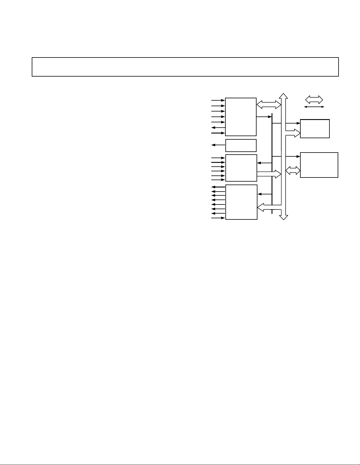
FUNCTIONAL BLOCK DIAGRAM
DATABUS
RESET
WR
A0–3
RD
CS
IRQ
CLK
REFOUT
REFIN
CONVST
AUX
PWMSYNC
AP
BP
CP
STOP
EMBEDDED
CONTROL
SEQUENCER
INTERNAL
REFERENCE
U
V
W
A
B
C
11-BIT
A/D
CONVERTER
12-BIT
PWM TIMER
BLOCK
D0 – D11
CONTROL BUS
CONTROL
REGISTERS
VECTOR
TRANSFORMATION
BLOCK
Flexible Analog Channel Sequencing
The ADMC200 support acquisition of 2, 3, or 4 channels per
group. Converted channel results are stored in registers and the
data can be read in any order. The sampling and conversion
time for two channels is 8 µs, three channels is 11.2 µs, and four
channels is 14.4 µs (using a 12.5 MHz system clock).
Embedded Control Sequencer
The embedded control sequencer off-loads the DSP or microprocessor, reducing the instructions required to read analog input channels, control PWM timers and perform vector transformations. This frees the host processor for performing control
algorithms.
Fast DSP/Microprocessor Interface
The high speed digital interface allows direct connection to
16-bit digital signal processors and microprocessors. The
ADMC200 has 12 bit memory mapped registers with twos
complement data format and can be mapped directly into the
data memory map of a DSP. This allows for a single instruction
read and write interface.
Integration
The ADMC200 integrates a four channel simultaneous sampling analog-to-digital converter, analog reference, vector transformation, and three-phase PWM timers into a 68-lead PLCC.
Integration reduces cost, board space, power consumption, and
design and test time.
REV. B
Information furnished by Analog Devices is believed to be accurate and
reliable. However, no responsibility is assumed by Analog Devices for its
use, nor for any infringements of patents or other rights of third parties
which may result from its use. No license is granted by implication or
otherwise under any patent or patent rights of Analog Devices.
One Technology Way, P.O. Box 9106, Norwood, MA 02062-9106, U.S.A.
Tel: 781/329-4700 World Wide Web Site: http://www.analog.com
Fax: 781/326-8703 © Analog Devices, Inc., 2000

(VDD = +5 V 5%; AGND = DGND = 0 V; REFIN = 2.5 V; External Clock =
ADMC200–SPECIFICATIONS
Parameter ADMC200AP Units Conditions/Comments
ANALOG-TO-DIGITAL CONVERTER
Resolution 11 Bits Twos Complement Data Format
Relative Accuracy ± 2 LSB max Integral Nonlinearity
Differential Nonlinearity ±2 LSB max
Bias Offset Error ± 5 LSB max Any Channel
Bias Offset Match 4 LSB max Between Channels
Full-Scale Error ± 6 LSB max Any Channel
Full-Scale Error Match 4 LSB max Between Channels
Conversion Time/Channel 40 System CLK Cycles
Signal-to-Noise Ratio (SNR)
2
Channel-to-Channel Isolation Sine Wave Applied to Unselected Channels
Two-/Three-Phase Mode –58 dB max
Three-/Three-Phase Mode –55 dB max
ANALOG INPUTS
Input Voltage Level 0–5 Volts
Analog Input Current 100 µA max
Input Capacitance 10 pF typ
TRACK AND HOLD
Aperture Delay 200 ns max Any Channel
Aperture Time Delay Match 20 ns max Between Channels
SHA Acquisition Time 20 System CLK Cycles
Droop Rate 5 mV/ms max
REFERENCE INPUT
Voltage Level 2.5 V dc
Reference Input Current 50 µA max
REFERENCE OUTPUT
Voltage Level 2.5 Volts
Voltage Level Tolerance ± 5 % max Full Load
Drive Capability ± 200 µA max
LOGIC
V
IL
V
IH
V
OL
V
OH
Input Leakage Current 1 µA max
Three-State Leakage Current 1 µA max
Input Capacitance 20 pF typ
PWM TIMERS
Resolution 12 Bits
Programmable Deadtime Range 0–10.08 µs
Programmable Deadtime Increments 2 System CLK Cycles 160 ns
Programmable Pulse Deletion Range 0–10.16 µs
Programmable Deletion Increments 1 System CLK Cycle 80 ns
Minimum PWM Frequency 1.5 kHz Resolution Varies with PWM Switching Frequency
VECTOR TRANSFORMATION Park & Clarke Transformation
Radius Error 0.7 % max
Angular Error 30 arc min max
Reverse Transformation Time 37 System CLK Cycles
Forward Transformation Time 40 System CLK Cycles
EXTERNAL CLOCK INPUT
Range 6.25–25 MHz If > 12.5 MHz, Then It Is Necessary to Divide Down
INTERNAL SYSTEM CLOCK
Range 6.25–12.5 MHz
POWER SUPPLY CURRENT
I
DD
NOTES
1
Measurements made with external reference.
2
Tested with PWM Switching Frequency of 25 kHz.
Specifications subject to change without notice.
1
60 dB min fIN = 600 Hz Sine Wave, f
0.8 V max
2.0 V min
0.4 V max I
4.5 V min I
20 mA max
12.5 MHz; TA = –40C to +85C unless otherwise noted)
SAMPLE
= 400 µA, VDD = 5 V
SINK
= 20 µA, VDD = 5 V
SOURCE
(10 MHz Clock: 20 kHz = 9 Bits, 10 kHz = 10 Bits,
5 kHz = 11 Bits, 2.5 kHz = 12 Bits). Higher Frequencies are Available with Lower Resolution
via SYSCTRL Register
= 55 kHz, 600 Hz
–2–
REV. B

ADMC200
Table I. Timing Specifications (VDD = 5 V 5%; TA = –4
0C to +85C)
Number Symbol Timing Requirements Min Max Units
1t
2t
3t
4t
5t
6t
7t
8t
9t
10 t
11 t
12 t
13 t
14 t
15 t
9
16 t
17 t
18 t
19 t
20 t
21 t
22 t
23 t
24 t
NOTE
1
All WRITES to the ADMC200 must occur within 1 system clock cycle (0 wait states).
clk CLK Period 40 160 ns
per
clk CLK Pulsewidth, High 20 ns
pwh
clk CLK Pulsewidth, Low 20 ns
pwl
csb_wrb CS Low before Falling Edge of WR 0ns
su
addr_wrb ADDR Valid before Falling Edge of WR 0ns
su
data_wrb DATA Valid before Rising Edge of WR 13 ns
su
wrb_data DATA Hold after Rising Edge of WR 4.5 ns
hd
wrb_addr ADDR Hold after Rising Edge of WR 4.5 ns
hd
wrb_csb CS Hold after Rising Edge of WR 4.5 ns
hd
1
wrb
pwl
1
wrb
pwh
wrb_clk_h
hd
wrb_clk_h
su
wrb_clk_l
su
clk_wrb_l
hd
csb_rdb CS Low before Falling Edge of RD 0ns
su
addr_rdb ADDR Valid before Falling Edge of RD 0ns
su
rdb_addr ADDR Hold after Rising Edge of RD 0ns
hd
rdb_csb CS Hold after Rising Edge of RD 0ns
hd
rdb RD Pulsewidth, Low 20 ns
pwl
rdb RD Pulsewidth, High 20 ns
pwh
rdb_clk_h RD Low before Rising Edge of CLK 7.5 ns
su
rdb_clk_h RD Low after Rising Edge of CLK 7.5 ns
hd
resetb RESET Pulsewidth, Low 2 × t
pwl
1
1
1
1
WR Pulsewidth, Low 20 ns
WR Pulsewidth, High 20 ns
WR Low after Rising Edge of CLK 7 ns
WR High before Rising Edge of CLK 7 ns
WR High before Falling Edge of CLK 10 ns
WR High after Falling Edge of CLK 10 ns
clk ns
per
Number Symbol Switching Characteristics Min Max Units
25 t
rdb_data DATA Valid after Falling Edge of RD 23 ns
dly
26 thdrdb_data DATA Hold after Rising Edge of RD 0ns
CLK
CLK
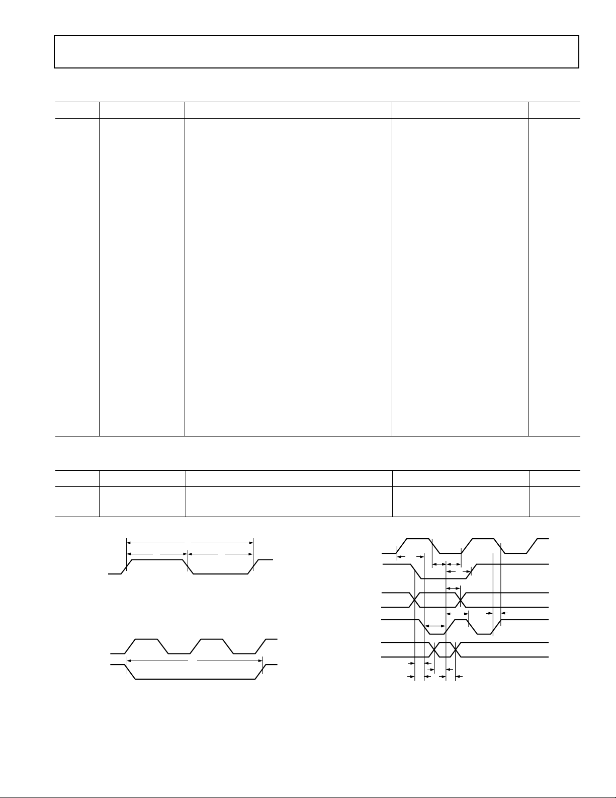
RESET
1
2
3
Figure 1. Clock Input Timing
24
Figure 2. Reset Input Timing
CLK
12
CS
A0–A3
WR
DATA
4
NOTE:
ALL WRITES TO THE ADMC200 MUST OCCUR WITHIN
ONE SYSTEM CLOCK CYCLE (i.e. 0 WAIT STATES)
5
13
15
9
8
11
10
6
7
14
Figure 3. Write Cycle Timing Diagram
REV. B
–3–

ADMC200
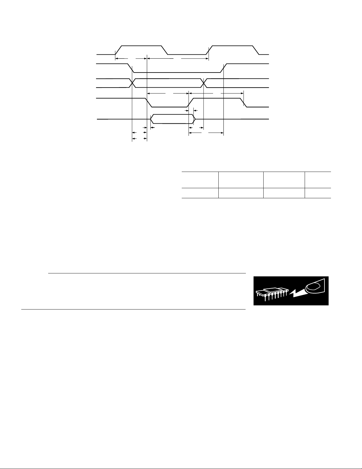
CLK
CS
A0–A3
23
22
20
RD
DATA
16
17
25
Figure 4. Read Cycle Timing Diagram
ABSOLUTE MAXIMUM RATINGS*
Supply Voltage (VDD) . . . . . . . . . . . . . . . . . . –0.3 V to +7.0 V
Digital Input Voltage . . . . . . . . . . . . . . . . . . . . . –0.3 V to V
Analog Input Voltage . . . . . . . . . . . . . . . . . . . . . –0.3 V to V
Analog Reference Input Voltage . . . . . . . . . . . . –0.3 V to V
Digital Output Voltage Swing . . . . . . . . . . . . . . –0.3 V to V
Analog Reference Output Swing . . . . . . . . . . . . –0.3 V to V
DD
DD
DD
DD
DD
Operating Temperature . . . . . . . . . . . . . . . . . –40°C to +85°C
Lead Temperature (Soldering, 10 sec) . . . . . . . . . . . . +280°C
*Stresses greater than those listed above may cause permanent damage to the
device. These are stress ratings only; functional operation of the device at these or
any other conditions greater than those indicated in the operational sections of this
specification is not implied. Exposure to absolute maximum rating conditions for
extended periods may affect device reliability.
21
26
18
19
ORDERING GUIDE
Part Temperature Package Package
Number Range Description Option
ADMC200AP –40°C to +85°C 68-Lead PLCC P-68A
CAUTION
ESD (electrostatic discharge) sensitive device. Electrostatic charges as high as 4000 V readily
accumulate on the human body and test equipment and can discharge without detection.
Although the ADMC200 features proprietary ESD protection circuitry, permanent damage may
occur on devices subjected to high energy electrostatic discharges. Therefore, proper ESD
precautions are recommended to avoid performance degradation or loss of functionality.
WARNING!
ESD SENSITIVE DEVICE
–4–
REV. B
 Loading...