

Page 1
PRELIMINAR Y TECHNICAL D A T A
Charge Pump Regulator & COM Driver
a
Preliminary Technical Data
FEATURES
Programmable COM Driver to prevent Screen-Burn
3 Voltages (5.0V,15.0V,-15.0V) from one 3V Supply
Power Efficiency optimised for use with TFT in mobile
phones
Low Quiescent Current
Low Shutdown Current (<5uA)
Shutdown Function
APPLICATIONS
Handheld Instruments
TFT LCD Panels
Cellular Phones
4.7F
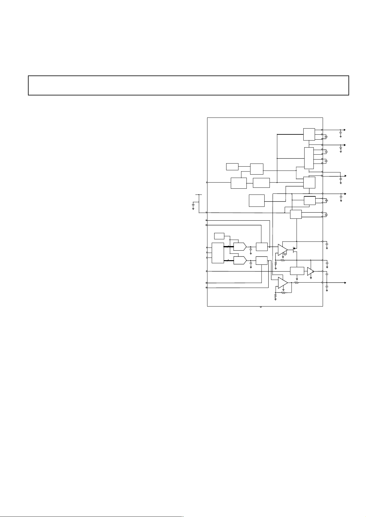
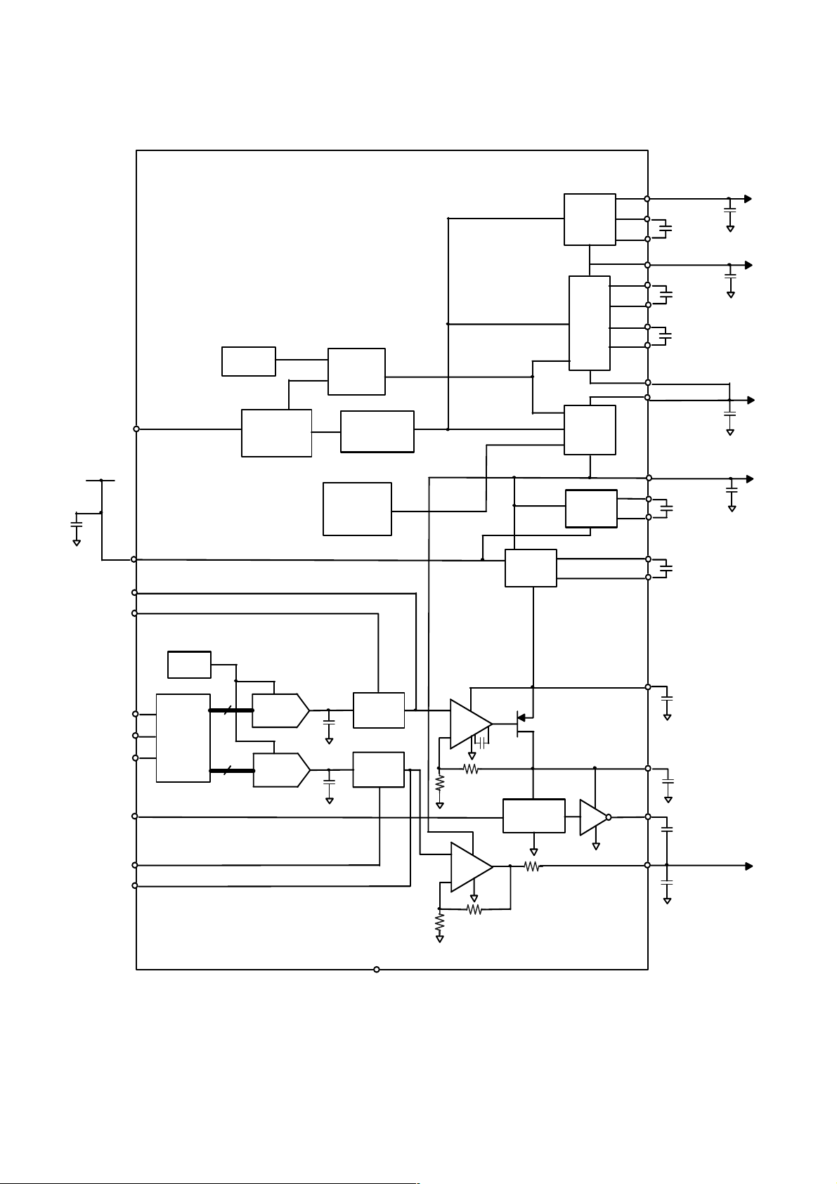
GENERAL DESCRIPTION
The ADM8840 combines a charge pump regulator and a
Common Line (COM) driver in a single chip solution for use
in TFT LCD’s. The device provides an LCD controller and
grayscale DAC supply voltage of 5.0V (±2%), 2 gate drive
voltages of +15V and -15V and a COM driver voltage. This
COM Driver voltage alternates the polarity of the Common
line voltage every line (or every frame) on the display in order
to prevent screen-burn occuring over time. The ADM8840
is powered by a single 3.0V supply.
The ADM8840 has an internal 100KHz oscillator for driving
the charge pumps.
The COM Driver section of the ADM8840 can be used to
generate the alternate frame or line inversion of the COM
line of the LCD panel. The ADM8840 receives the COM
clock from the controller with a frequency up to 10kHz and
allows programmable conditioning of its amplitude and
centre voltage through the use of on-board DAC’s. This
allows programmable elimination of display flicker caused
by the COM inversion.
The COM_OUT amplitude can be programmed from 4.0V
to 7.0V in steps of 28mV. The COM_OUT centre voltage
can be programmed to 0.9V to 2.8V in steps of 14mV.
for Color TFT Panel
ADM8840
FUNCTIONAL BLOCK DIAGRAM
-15V
C9
5VO UT
C4
0.22F
C2
0.22
C3
0.22
C1
3.3
3.3
C11
C12
C13
22nF
0.22F
+15V
C8
0.22
F
F
+5V
C7
2.2F
VOUT
C10
3.3
F
F
C5
F
4.7F
4.7F
4.7
F
COM_OUT
C
PANEL
TM
).
VOLTAGE
C4+
INVER T ER
ADM8840
OSCILLATOR
VREF
SHUTDOWN
CONTROL
8
8
SHDN
C6
V
CC
DAC1_IN
DAC1_SD
CLK
SERIAL
DATA
INTERFACE
CS/
LDAC
COM_I N
DAC2_SD
DAC2_IN
DAC 1
DAC 2
TIMING
GENERATOR
DISCHA RGE
CONTROL
LOGIC
INT/EXT
DAC 1
INT/EXT
DAC 2
GND
REGUL ATOR
VOLTAGE
ADDER
+
-
LEVEL
TRANSLATOR
+
5.5k
-
⍀
TRIPLE
VOLTAGE
TRIPLER
DOUBLE
LDO
VOLTAGE
VOLTAGE
DOUBLER
POWER
BUFFER
C4-
C2+
C2-
C3+
C3-
5VIN
C1+
C1-
C5+
C5-
ADD_OUT
TRANS_OUT
COM_OUT_AC
The ADM8840 provides power up sequencing of the -15V
and +15V gate drive outputs, ensuring the -15V starts to
power up before the +15V.
The ADM8840 has a number of power save features, including low power Shutdown. The 5.0V output consumes the
most power, so Power Efficiency is also maximised on this
output with an oscillator enabling scheme (Green Idle
The ADM8840 is fabricated using CMOS technology for
minimal power consumption. The part is packaged in a 32pin LFCSP package.
F
REV. PrG 2/03
Information furnished by Analog Devices is believed to be accurate and
reliable. However, no responsibility is assumed by Analog Devices for its
use, nor for any infringements of patents or other rights of third parties
which may result from its use. No license is granted by implication or
otherwise under any patent or patent rights of Analog Devices.
TM
Green Idle is a registered trademark of Analog Devices Inc.
One Technology Way, P.O. Box 9106, Norwood, MA 02062-9106, U.S.A.
Tel: 781/329-4700 World Wide Web Site: http://www.analog.com
Fax: 781/326-8703 Analog Devices, Inc., 2003
Page 2
ADM8840
SHDN
C6
4.7F
DAC1_IN
DAC1_SD
PRELIMINAR Y TECHNICAL D A T A
-15V
C9
C8
C7
VOUT
+15V
0.22F
0.2 2
+5V
2.2F
C10
3.3
F
F
VOLTAGE
INVERTER
ADM8840
TRIPLE
VOLTAG E
TRIPLER
DOUBLE
OSCILLATOR
SHUTDOWN
CONT RO L
V
CC
TIMING
GENERATOR
DISCHAR G E
CO NT RO L
LOGIC
VOLTAGE
ADDER
LDO
VOLTAGE
REG UL ATOR
VOLTAG E
DOUBLER
C4+
C4-
C2+
C2-
C3+
C3-
5VIN
5VO U T
C1+
C1-
C5+
C5-
C4
0.22F
C2
0.22
C3
0.22
C1
3.3
C5
3.3
F
F
F
F
CLK
DATA
CS /
LDAC
COM_IN
DAC2_SD
DAC2_IN
VREF
SERIAL
INTERFACE
8
8
DAC 1
DAC 2
INT /EXT
DAC 1
INT/EXT
DAC 2
GND
+
-
+
-
ADM8840 FUNCTIONAL BLOCK DIAGRAM
LEVEL
TRANS L ATOR
5.5k
⍀
POWER
BUFFER
ADD_OUT
C11
4.7F
TRANS_OUT
C12
4.7F
COM_OUT_AC
C13
F
4.7
C
PANEL
22nF
COM_OUT
–2– REV. PrG 2/03
Page 3

PRELIMINAR Y TECHNICAL D A T A
(VCC = +3V-10%,+20%, TA=-40°C to +85°C unless otherwise noted )
C1,C5,C10=3.3
F; C2,C3,C4,C8,C9=0.22
PARAMETER Min Typ Max Units Test Conditions
Input Voltage,V
Supply Current,I
CC
CC
CHARGE PUMP REGULATOR
+5.0V OUTPUT
Output Voltage 4.9 5.0 5.1 V I
Output Current 5 mA
Output Ripple 10 mV p-p 5mA load
Transient Response 5 us I
+15.0V OUTPUT
Output Voltage 14.0 15.0 16.0 V I
Output Current 50 150 uA
Output Ripple 50 mV p-p I
-15.0V OUTPUT
Output Voltage -16.0 -15.0 -14.0 V I
Output Current -150 -5 0 uA
Output Ripple 50 mV p-p I
Charge-Pump Frequency T BD 100 TB D kHz
DIGITAL INPUT PINS
Input Voltage, V
IH
Digital Input Current 1 A
Digital Input Capacitance 10 pF Note 1.
COM DRIVER
COM_OUT
Amplitude 4 7 V
Amplitude Stepsize 28 mV
Amplitude Accuracy <10% % V
Center Voltage 0.9 1.8 2.8 V
Center Voltage Stepsize 14 m V
Center Voltage Accuracy <10% % V
Rise/Fall Time 1 sC
Center Voltage Settling Time TBD us
PANEL
Load Capacitance 20 nF
POWER EFFICIENCY 70 % 5V
NOTES
1. Guaranteed by Design. Not 100% Production Tested.
2. COM Driver load is defined as the load current flowing through C13 with DACs loaded with preset values.
* Specifications are target values and are subject to change without notice.
F; C6,C11,C12,C13=4.7
F; C7 =2.2
F
2.7 3.3 3.6 V
750 uA O/Ps Unloaded; COM_IN Low;
5 uA Shutdown Mode
0.7V
CC
0.3V
CC
ADM8840-SPECIFICATIONS
DAC1_SD, DAC2_SD Low
DAC1_IN and DAC2_IN should
be open circuit because there
is a voltage on these pins due to
the output of the DAC.
= 10uA to 5mA
L
stepped from 10uA to 5mA
L
= 1uA to 100uA
L
=100uA
L
= -1uA to -100uA
L
=-100uA
L
V
V
COM_OUT
DAC1 loaded with preset values;
Measured at TRANS_OUT
DAC1 preset values is 1V and
Vcom should be 6V
CENTER
DAC2 loaded with preset values
DAC2 preset values is 500mV and
Vcentre should be 1.5V.
PANEL
OUT
+/-15V Load = +/-100uA;
COM_IN Freq = 10kHz;
C
PANEL
Vcc=2.7V;
Note 2
=5V;
=1.8V;
=20nF
Load = 5mA;
= 20nF;
–3–REV. PrG 2/03
Page 4

ADM8840
PRELIMINAR Y TECHNICAL D A T A
Timing Specifications
VCC = +3V-10%,+20%, TA=-40°C to +85°C
PARAMETER Min Typ Max Units Test Conditions /Comments
POWER-UP SEQUENCE
5V Rise time, T
+15V Rise time, T
-15V Fall time, T
Delay between V
and SHDN rise, T
CC
R5V
R15V
F15V
rise
DELAY1
TBD us 10% to 90%, Figure 2
TBD ms 10% to 90%, Figure 2
TBD ms 90% to 10%, Figure 2
TBD ms Figure 2
Delay between -15V fall
and +15V rise, T
DELAY2
TBD ms Figure 2
POWER- DOWN SEQUENCE
5V Fall time, T
F5V
+15V Fall time, T
-15V Rise time, T
R15V
F15V
TBD ms 90% to 10%, Figure 2
TBD ms 90% to 10%, Figure 2
TBD ms 10% to 90%, Figure 2
SERIAL INTERFACE
t1 TBD ns CS/LDAC falling edge to SCLK
Rising Edge; Note 1; Note2
t2 T BD ns SCLK High Pulsewidth; Note 1; Note2
t3 T BD ns SCLK Low Pulsewidth; Note 1; Note2
t4 TBD ns Minumum CS/LDAC high time;
Note 1; Note2
t5 TBD ns SCLK Rising Edge to CS/LDAC
Rising Edge; Note 1; Note2
t6 T BD ns DATA Setup time; Note 1; Note2
t7 T BD ns DATA Hold time; Note 1; Note2
NOTES
1. Guaranteed by Design. Not 100% Production Tested.
2. See Timing Diagram in Figure 4.
* Specifications are target values and are subject to change without notice.
ABSOLUTE MAXIMUM RATINGS*
(TA=25oC unless otherwise noted.)
Supply Voltage -0.3 V to +4.0 V
Input Voltage on Digital Inputs -0.3 V to +4.0 V
Model Temperature Package
ADM8840ACP -40°C to +85°C CP-32
ORDERING GUIDE
Range Option
Output Short Circuit Duration to GND 10 seconds
Output Voltage
+5.0V Output -0.3 V to +6.0 V
PIN CONFIGURATION
-15.0V Output -17 V to +0.3 V
+15.0V Output -0.3 V to +17 V
Operating Temperature Range -40°C to +85°C
Power Dissipation 50mW
Storage Temperature Range -65°C to +150°C
E S D Class I
*Stresses above those listed under “Absolute Maximum Ratings” may
cause permanent damage to the device. This is a stress rating only;
functional operation of the device at these or any other conditions above
those indicated in the operational section of this specification is not
implied. Exposure to absolute maximum rating conditions for extended
periods may affect device reliability.
THERMAL CHARACTERISTICS
C1+
V
VOUT
5VOUT
5VIN
SHDN
DAC1_SD
DAC2_SD
GND
C1-
32
31
1
2
CC
3
4
5
6
7
8
(NOT TO SCALE)
-15VOUT
30
29
ADM8840
TOP VIEW
C4+
C4-
C2-
C2+
C3+
25
26
2728
24
C3-
15VOUT
23
V
22
CC
C5-
21
C5+
20
19
ADD_OUT
COM_IN
18
GND
17
32-Lead LFCSP Package:
⍜
= 28°C/Watt
JA
11
9
12
10
13
16
15
14
SCLK
DATA
DAC2_IN
DAC1_IN
CS/LDAC
COM_OUT
TRANS_OUT
COM_OUT_AC
–4– REV. PrG 2/03
Page 5

PRELIMINAR Y TECHNICAL D A T A
ADM8840
PIN FUNCTION DESCRIPTION
Pin Mnemonic Function
1,32 C1+,C1- External capacitor C1 is connected between these pins. A 3.3F capacitor is
recommended.
2, 22
3 VOUT Voltage Doubler Output. This was derived by doubling the 3V supply. A 3.3F
4 +5VOUT +5.0V output pin. This was derived by doubling and regulating the +3V supply.
5 +5VIN +5.0V input pin. This is the input to the voltage tripler and inverter charge pump
6 SHDN Digital Input. 3V CMOS Logic. Active low shutdown control. This shuts down
7 DAC1_SD Switches over to external DAC1 input when asserted.
9 DAC1_IN Input for external DAC1 signal.
17, 31 G N D Device Ground Pin.
V
CC
Positive Supply Voltage Input. Connect this pin to 3V supply. A 4.7F
decoupling capacitor should be attached close to pin 2.
capacitor to ground is required on this pin.
A 2.2F capcitor to ground is required on this pin to stabilise the regulator.
circuits.
the timing generator and enables the discharge circuit to dissipate the charge on
the voltage outputs, thus driving them to 0V.
13 SCL K External Clock Input. Used to load DAC 1 with COM Voltage amplitude and
DAC 2 with COM Centre Voltage.
12 DATA Digital Data Input to both DAC’s 1 and 2.
11 CS / LDAC Dual function pin.
1.Chip Select. Digital Input Logic. Chip Select for Digital Interface.
2. Load DAC. Digital Input Logic. DAC’s 1 and 2 perform a conversion on a
low-to-high transition.
18 COM_IN Clock Input from digital controller chip. This input is level shifted, offset and
inverted to provide a COM Voltage output swing at a frequency of the COM_IN
input.
16 COM_OUT_AC COM_OUT_AC outputs the COM_IN signal inverted and level shifted by the
value programmed on DAC 1. A 4.7F capacitor is connected between this pin
and COM_OUT.
14 COM_OUT The AC output on COM_OUT_AC is added to the center voltage programmed on
DAC2 so that the desired amplitude, centered about the correct center voltage
appears on COM_OUT. The load capacitance seen by this pin is the bulk capaci
tance of the panel, typically 20nF.
8 DAC2_SD Switches over to external DAC2 input when asserted.
10 DAC2_IN Input for external DAC2 signal.
15 TRANS_OUT Level Translator Reference Output Voltage. This is the voltage that the value on
DAC 1 is gained up to to provide the upper voltage for the Level Translator. A
voltage of between 4.0V and 7.0V can be output here. A 4.7F cap is
recommended for this pin.
CAUTION
ESD (electrostatic discharge) sensitive device. Electrostatic charges as high as 4000 V readily
accumulate on the human body and test equipment and can discharge without detection.
Although the ADM8840 features proprietary ESD protection circuitry, permanent damage
may occur on devices subjected to high energy electrostatic discharges. Therefore, proper
ESD precautions are recommended to avoid performance degradation or loss of functionality.
–5–REV. PrG 2/03
Page 6

PRELIMINAR Y TECHNICAL D A T A
ADM8840
PIN FUNCTION DESCRIPTION (Contd.)
Pin Mnemonic Function
19 ADD_OUT Voltage Adder Output Pin. This is voltage generated by adding VOUT
(unregulated output of first stage doubler) to V
then used as the supply for the gain stage which generates the Level
Translator Output Voltage. A 4.7F capacitor is recommended for this pin.
20,21 C5+,C5- External capacitor C5 is connected between these pins. A 3.3F capacitor is
recommended.
23 +15VOUT +15.0V output pin. This was derived by tripling the +5.0V regulated output. A
0.22F capacitor is required on this pin.
29,28 C4+,C4- External capacitor C4 is connected between these pins. A 0.22F capacitor is
recommended.
25,24 C3+,C3- External capacitor C3 is connected between these pins. A 0.22F capacitor is
recommended.
27,26 C2+,C2- External capacitor C2 is connected between these pins. A 0.22F capacitor is
recommended.
. This summed voltage is
CC
30 -15VOUT -15.0V output pin. This was derived by inverting the +15.0V output. A
0.22F capacitor is required on this pin.
COM_OUT VOLTAGE
The COM Driver section of the ADM8840 can be used to
generate the alternate frame or line inversion of the COM
line of the LCD panel. The ADM8840 receives the COM
clock (with frequency up to 10kHz) from the controller and
allows programmable conditioning of its amplitude and
centre voltage through the use of on-board DAC’s 1 and 2.
This allows programmable elimination of display flicker
caused by the COM inversion.
The COM_OUT amplitude can be programmed from 4.0V
to 7.0V in steps of 28mV. The COM_OUT centre voltage
can be programmed from 0.9V to 2.8V in steps of 14mV.
Figure 1 below shows a typical output from the COM_OUT
POWER SEQUENCING
In order for the TFT panel to power up correctly, the gate
drive supplies must be sequenced such that the -15V supply
starts up before the +15V supply. The ADM8840 controls
this sequence. When the device is turned on, the ADM8840
allow the -15V output to ramp immediately, but holds off the
+15V output. It continues to do this until the negative output
has reached -3V. At this point, the positive output is enabled
and allowed to ramp to +15V. This sequence is highlighted
in figure 2.
t
DEL AY1
V
CC
pin. If programmable operation is not required the DACs can
be shutdown with the DAC1_SD and DAC2_SD pins and an
analog voltage applied to the DAC1_IN and DAC2_IN pins
to set up the amplitude and centre voltage at COM_OUT.
4.0V to 7.0V
0.9V->1.8V->2.8V
0V
Figure 1. COM_OUT Voltage
SHDN
+5V
+15V
-15V
AMPLITUDE:
4.0V to 7.0V
COM_OUT
0V
10%
t
R5V
90%
10%
t
R15V
90%
10%
t
DELAY2
90%
t
FM15V
-3V
t
F5V
t
F15V
t
RM15V
CENTRE
VOLTAGE:
0.9V->1.8 V->2.8V
Figure 2. Power Sequence
–6– REV. PrG 2/03
Page 7

PRELIMINAR Y TECHNICAL D A T A
ADM8840
SERIAL INTERFACE
The COM Driver section of the ADM8840 uses a serial
interface to input data and transfer it into the DACs. Figure
3, below, shows the operation of the serial interface. The data
is transmitted along the serial DATA line, along with a serial
clock signal, SCLK. This data is read into a Shift Register.
When the 8 bits are sucessfully stored in the Shift Register a
low-to-high transition on the CS/LDAC input causes the
latch to load the 8-bits of data into the relevent DAC.
This function is also shown in the waveforms in Figure 4
below. A falling edge on the CS/LDAC input initiates the
data read into the shift register. The first bit of the datastream
is the DAC Select Bit (DAC_SEL) which determines which
internal DAC the data will be written to. A ‘1’ selects DAC
1 which sets the Amplitude of the output and a ‘0’ selects
8DATABITS
DATA
SCLK
SHIFT
REGISTER
DAC_SEL BIT
DAC1
LATCH
DAC 2 which sets the Centre Voltage of the output. The
individual data bits are then read in one by one on the DATA
line. After the DAC_SEL bit and the 8 data bits have been
read there is a pause to ensure the shift register outputs are
stable. Then a rising edge on the CS/LDAC input loads the
8 bits on the shift register outputs into the relevent DAC (and
the DAC outputs will change accordingly). Note that if CS/
LDAC goes high before all 8 data bits are read in then
incorrect data will be loaded into the DACs. All bits on the
DATA line are read in on each rising edge of the SCLK
signal.
When the ADM8840 comes out of shutdown the DACs
are preset with default values generating a COM_OUT
Amplitude of 6V with a Centre voltage of 1.5V.
DAC 1
(AMPLITUDE)
DAC 1 OUT
CS/LDAC
CS /
LDAC
SCLK
DATA
DAC
SELECT
DAC 2
LATCH
DAC 2
(CENTRE VOLTAGE)
DAC 2 OUT
Figure 3. Serial Interface Diagram
t
1
DAC
SEL
D0 D1
D2 D 3 D4 D5 D6
t
3
t
2
D7
t
4
t
7
t
6
Figure 4. Serial Interface Waveforms
–7–REV. PrG 2/03
t
5
Page 8

ADM8840
PRELIMINAR Y TECHNICAL D A T A
DAC1 Setup
The resolution of DAC1 is 4.7mV this is scaled up by 6 to
give COM_OUT amplitude resolution of 28mV (4.7mV *
6 = 28mV). The COM_OUT amplitude Vp-p is given by,
(Binary Code/255)(1.188)(6)= Vp-p (COM_OUT).
A table of the min, max and typical values for COM_OUT
amplitude is given in the Table 1 below.
Table 1 COM_OUT amplitude Voltage
COM_OUT amplitude voltage Binary Bits written to DAC1 Integer DAC1_IN Voltage
(Max) 7.016V 11111011 251 1.667V
6.9882 11111010 250 1.6623
......... ............. ..... ...........
(Typ) 6.0098V 11010111 215 1.0011V
.......... ............. ..... ...........
4.0531V 10010001 145 671.7mV
(Min) 4.0025V 10010000 144 667mV
Table 2 COM_OUT centre voltage
COM_OUT centre voltage Binary Bits written to DAC2 Integer DAC2_IN Voltage
DAC2 Setup
The resolution of DAC2 is 4.7mV this is scaled up by 3 to
give you the COM_OUT centre voltage resolution of
14mV (4.7mV * 3 = 14mV). The COM_OUT centre
voltage is given by,
(Binary Code/255)(1.188)(3)= COM_OUT DC Voltage.
A table of the min, max and typical values for COM_OUT
centre voltage is given in the Table 2 below.
(Max) 2.8092V 11001001 201 933mV
2.7952V 11001000 200 928mV
........... .............. ...... ..........
(Typ) 1.5094V 01101100 108 503.9mV
........... .............. ...... ..........
0.9224V 01000010 66 304.7mV
(Min) 0.9084V 01000001 65 300mV
–8– REV. PrG 2/03
Page 9

PRELIMINAR Y TECHNICAL D A T A
ADM8840
BOOSTING THE CURRENT DRIVE OF THE +/-15V
SUPPLY
The ADM8840 +/-15V output can deliver 100uA of
typical
current in the
configuration, as shown in Figure
5.
In this configuration the 5Vout (pin 4) is connected to
5Vin (pin 5), as can be seen on block diagram Page 1 of
this data sheet.
-15V
VOLTAGE
INVER T ER
ADM8840
TRIPLE
VOLTAGE
TRIPLER
VOLTAGE
ADDER
DOUBLE
LDO
VOLTAGE
REGUL ATOR
VOLTAGE
DOUBLER
OSCILLATOR
SHDN
C6
4.7F
V
CC
DAC1_IN
DAC1_SD
SHUTDOWN
CONTROL
TIMING
GENERATOR
DISCHA RGE
CONTROL
LOGIC
C9
C4+
C4
0.22F
C4-
+15V
C8
C2+
C2
0.22
F
C2-
C3+
C3
0.22
F
C3-
5VIN
5VO UT
C7
VOUT
C1+
C1
3.3
F
C1-
C5+
C5
3.3
F
C5-
It is possible to configure the ADM8840 to supply up to
400uA on the +/-15V outputs, by changing its
configuration slightly, as shown in Figure 6.
VOLTAGE
INVERTER
0.22F
0.22
ADM8840
OSCILLATOR
SHDN
C6
4.7F
V
F
+5V
2.2F
C10
3.3
F
DAC1_IN
DAC1_SD
CS/
COM_IN
DAC2_SD
DAC2_IN
CC
CLK
DATA
INTERFACE
LDAC
SHUTDOWN
VREF
8
SERIAL
8
CONTROL
DAC 1
DAC 2
TIMING
GENERATOR
DISCHARGE
CONTROL
LOGIC
INT/EXT
DAC 1
INT/EX T
DAC 2
+
-
+
-
VOLTAGE
ADDER
LEVEL
TRAN SLATOR
5k
⍀
TRIPLE
VOLTAGE
TRIPLER
DOUBLE
LDO
VOLTAGE
REGULATOR
VOLTAGE
DOUBLER
POWER
BUFFER
C4+
C4
0.22F
C4-
C2+
C2
0.22
C2-
C3+
C3
0.22
C3-
5VIN
5VOUT
C1+
C1
3.3
C1-
C5+
C5
3.3
C5-
ADD_O UT
C11
4.7F
TRANS_ OUT
C12
4.7F
COM_OUT_AC
C13
4.7
C
22nF
-15V
C9
+15V
C8
F
Current Boost
F
Configuration
Connection
C7
VOUT
F
F
F
COM_OUT
PANEL
0.22F
0.22
F
+5V
2.2F
C10
3.3
F
CS/
COM_I N
DAC2_SD
DAC2_IN
VREF
8
CLK
SERIAL
DATA
INTERFACE
LDAC
DAC 1
8
DAC 2
INT/EXT
DAC 1
INT/EXT
DAC 2
+
-
LEVEL
TRANSLATOR
+
5k
⍀
-
POWER
BUFFER
ADD_OUT
C11
4.7F
TRANS_OUT
C12
4.7F
COM_OUT_AC
C13
4.7
C
22nF
PANEL
GND
Figure 6. Current Boost Configuration
The configuration in Figure 6, can supply up to 400uA of
F
COM_OUT
current on both the +15V and the -15V outputs. If the
load on the +/-15V does not draw any current the voltage
on the +/-15V outputs can rise up to +/-16.5V.In this
configuration Vout (pin 3) is connected to 5Vin (pin 5).
GND
Figure 5. Typical Configuration
–9–REV. PrG 2/03
Page 10

ADM8840
2
4
PRELIMINAR Y TECHNICAL D A T A
OUTLINE DIMENSIONS
Dimensions Shown in Inches and (mm).
32-Lead 5X5 Chip Scale Package
PIN 1
INDICATOR
0.035 (0.90) MAX
0.033 (0.85) NOM
SEATING
PLANE
12. MAX
0.197 (5.0)
BSC SQ
TOP
VIEW
0.020 (0.50)
BSC
(CP-32)
0.187 (4.75)
BSC SQ
0.031 (0.80) MAX
0.026 (0.65) NOM
0.002 (0.05)
0.0004 (0.01)
0.008(0.20)
REF
0.0 (0.00)
0.024 (0.60)
0.017 (0.42)
0.009 (0.24)
0.012 (0.30)
0.009 (0.23)
0.007 (0.18)
0.020 (0.50)
0.016 (0.40)
0.012 (0.30)
0.0
(0.60)
0.017 (0.42)
0.009 (0.24)
25
24
17
16
0.138 (3.50)
BOTTOM
VIEW
REF
0.010 (0.25)
MIN
32
1
8
9
0.128 (3.25)
0.122 (3.10) SQ
0.116 (2.95)
–10– REV. PrG 2/03
 Loading...