

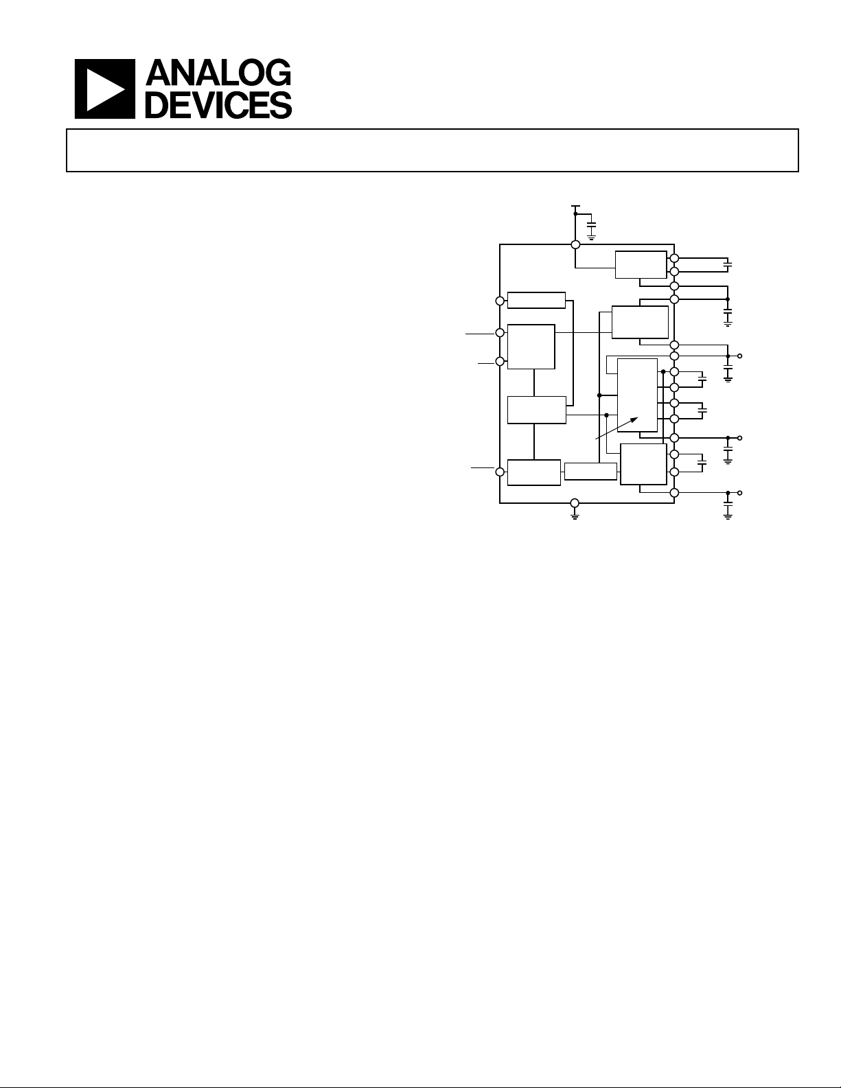
Charge Pump Regulator
FEATURES
3 output voltages (+5.1 V, +15.3 V, −10.2 V) from one 3 V
input supply
Power efficiency optimized for use with TFT in mobile
phones
Low quiescent current
Low shutdown current (<1 µA)
Fast transient response
Shutdown function
Power saving during blanking period
Option to use external ldo
APPLICATIONS
Handheld instruments
TFT LCD panels
Cellular phones
GENERAL DESCRIPTION
The ADM8832 is a charge pump regulator used for color thin
film transistor (TFT) liquid crystal displays (LCD). Using charge
pump technology, the device can be used to generate three
output voltages (+5.1 V ±2%, +15.3 V, −10.2 V) from a single
3 V input supply. These outputs are then used to provide
supplies for the LCD controller (+5.1 V) and the gate drives for
the transistors in the panel (+15.3 V and −10.2 V). Only a few
external capacitors are needed for the charge pumps. An
efficient low dropout voltage regulator also ensures that the
power efficiency is high and provides a low ripple 5.1 V output.
This LDO can be shut down and an external LDO used to
regulate the 5 V doubler output and drive the input to the
charge pump section, which generates the +15.3 V and −10.2 V
outputs if so required by the user.
The ADM8832 has an internal 100 kHz oscillator for use in
scanning mode, but the part must be clocked by an external
clock source in blanking (low current) mode. The internal
oscillator is used to clock the charge pumps during scanning
for Color TFT Panel
ADM8832
FUNCTIONAL BLOCK DIAGRAM
C5
CC
TRIPLER
DISCHARGE
GND
2.2µF
VOLTAGE
DOUBLER
VOLTAGE
REGULATOR
DOUBLE
INVERTER
Figure 1.
LDO
TRIPLE
VOLTAGE
C1+
C1–
VOUT
LDO IN
+5VOUT
+5VIN
C2+
C2–
C3+
C3–
+15VOUT
C4+
C4–
–10VOUT
C2
1µF
C3
1µF
C4
1µF
C1
2.2µF
C6
2.2µF
+5.1V
C7
2.2µF
+15.3V
C8
1µF
–10.2V
C9
1µF
V
ADM8832
OFF
SHDN
OSCILLATOR
CONTROL
LOGIC
TIMING
GENERATOR
SHUTDOWN
CONTROL
VOLTAGE
CLKIN
SCAN/
BLANK
LDO_ON/
mode where the current is highest. During blanking periods, the
ADM8832 switches to an external, lower frequency clock. This
allows the user to vary the frequency and maximize power
efficiency during blanking periods. The tolerances on the output
voltages are seamlessly maintained when switching from scanning mode to blanking mode or vice versa.
The ADM8832 power saving features include low power
shutdown and reduced quiescent current consumption during
the blanking periods. The 5.1 V output consumes the most
power, so power efficiency is also maximized on this output
with an oscillator enabling scheme (Green Idle™). This
effectively senses the load current that is flowing and turns on
the charge pump only when charge needs to be delivered to the
5 V pump doubler output.
The ADM8832 is fabricated using CMOS technology for minimal
power consumption. The part is packaged in a 20-lead LFCSP
(lead frame chip scale package).
03759-A-001
Rev. A
Information furnished by Analog Devices is believed to be accurate and reliable.
However, no responsibility is assumed by Analog Devices for its use, nor for any
infringements of patents or other rights of third parties that may result from its use.
Specifications subject to change without notice. No license is granted by implication
or otherwise under any patent or patent rights of Analog Devices. Trademarks and
registered trademarks are the property of their respective owners.
One Technology Way, P.O. Box 9106, Norwood, MA 02062-9106, U.S.A.
Tel: 781.329.4700 www.analog.com
Fax: 781.326.8703 © 2004 Analog Devices, Inc. All rights reserved.

ADM8832
TABLE OF CONTENTS
Specifications..................................................................................... 3
Theory of Operation ...................................................................... 10
Timing Specifications .................................................................. 4
Absolute Maximum Ratings............................................................ 5
Thermal Characteristics .............................................................. 5
ESD Caution.................................................................................. 5
Pin Configuration and Function Descriptions............................. 6
Typical Performance Characteristics ............................................. 7
REVISION HISTORY
4/04—Changed from Rev. 0 to Rev. A
Changes to Outline Dimensions................................................... 11
Updated Ordering Guide............................................................... 11
7/03—Revision 0: Initial Version
Scanning and Blanking.............................................................. 10
Power Sequencing...................................................................... 10
Transient Response .................................................................... 10
External Clock ............................................................................ 10
Outline Dimensions....................................................................... 11
Ordering Guide .......................................................................... 11
Rev. A | Page 2 of 12
ADM8832
SPECIFICATIONS
VCC = 2.6 V to 3.6 V, TA = −40°C to +85°C, unless otherwise noted; C1, C5, C6, C7 = 2.2 µF, C2, C3, C4, C8, C9 = 1 µF, CLKIN = 1 kHz in
blanking mode.
Table 1.
Parameter Min Typ Max Unit Test Conditions
INPUT VOLTAGE, VCC 2.6 3.6 V
SUPPLY CURRENT, ICC 150 400 µA Unloaded, Scanning Period
70 140 µA Unloaded, Blanking Period
1 µA Shutdown Mode, TA = 25°C
+5.1 V OUTPUT
Output Voltage 5.0 5.1 5.2 V IL = 10 µA to 8 mA
Output Current 4 5 mA Scanning Period
5 8 mA Scanning Period, VCC > 2.7 V
50 200 µA Blanking Period
Power Efficiency 80 % VCC = 3 V, IL = 5 mA (Scanning)
70 % VCC = 3 V, IL = 200 µA (Blanking)
Output Ripple 10 mV p-p 8 mA Load
Transient Response 5 µs IL Stepped from 10 µA to 8 mA
+15.3 V OUTPUT
Output Voltage 14.4 15.3 15.6 V IL = 1 µA to 100 µA
Output Current 50 100 µA Scanning Period
1 10 µA Blanking Period
Output Ripple 50 mV p-p IL = 100 µA
−10.2 V OUTPUT
Output Voltage −10.4 −10.2 −9.6 V IL = –1 µA to −100 µA
Output Current −100 −50 µA Scanning Period
−10 −1 µA Blanking Period
Output Ripple 50 mV p-p IL = –100 µA
POWER EFFICIENCY 90 % Relative to 5.1 V Output, IL = 100 µA (Scanning)
(+15.3 V and −10.2 V Outputs) 80 % Relative to 5.1 V Output, IL = 10 µA (Blanking)
CHARGE PUMP FREQUENCY 60 100 140 kHz Scanning Period
CONTROL PINS
SHDN
Input Voltage, V
0.7 VCC V
Digital Input Current ±1 µA
Digital Input Capacitance1 10 pF
SCAN/BLANK
Input Voltage 0.3 VCC V
0.7 VCC V High = SCAN Period
Digital Input Current ±1 µA
Digital Input Capacitance1 10 pF
LDO_ON/OFF
Input Voltage 0.3 VCC V Low = External LDO
0.7 VCC V High = Internal LDO
Digital Input Current ±1 µA
Digital Input Capacitance1 10 pF
Footnotes after table.
0.3 VCC V
SHDN
Low = Shutdown Mode
SHDN
High = Normal Mode
SHDN
Low = BLANK
Period
Rev. A | Page 3 of 12

ADM8832
Parameter Min Typ Max Unit Test Conditions
CLKIN
Minimum Frequency 0.9 1 kHz Duty Cycle = 50%, Rise/Fall Times = 20 ns
Input Voltage
VIL 0.3 VCC V
VIH 0.7 VCC V
Digital Input Current ±1 µA
Digital Input Capacitance1 10 pF
1
Guaranteed by design. Not 100% production tested.
Specifications are subject to change without notice.
TIMING SPECIFICATIONS
VCC = 2.6 V to 3.6 V, TA = –40°C to +85°C, unless otherwise noted; C1, C5, C6, C7 = 2.2 µF, C2, C3, C4, C8, C9 = 1 µF, CLKIN = 1 kHz in
blanking mode.
Table 2.
Parameter Min Typ Max Unit Test Conditions/Comments
POWER-UP SEQUENCE
+5 V Rise Time, t
+15 V Rise Time, t
−10 V Fall Time, t
Delay between −10 V Fall and +15 V, t
POWER-DOWN SEQUENCE
+5 V Fall Time, t
+15 V Fall Time, t
−10 V Rise Time, t
300 µs 10% to 90%, Figure 17
R5V
8 ms 10% to 90%, Figure 17
R15V
12 ms 90% to 10%, Figure 17
F10V
3 ms Figure 17
DELAY
75 ms 90% to 10%, Figure 17
F5V
40 ms 90% to 10%, Figure 17
F15V
40 ms 10% to 90%, Figure 17
R10V
Rev. A | Page 4 of 12

ADM8832
ABSOLUTE MAXIMUM RATINGS
TA = 25°C, unless otherwise noted.
Table 3.
Parameter Ratings
Supply Voltage −0.3 V to +4.0 V
Input Voltage to Digital Inputs −0.3 V to +4.0 V
Output Short Circuit Duration to GND 10 sec
Output Voltage
+5.1 V Output −0.3 V to +6 V
−10.2 V Output −12 V to +0.3 V
+15.3 V Output −0.3 V to +17 V
Operating Temperature Range −40°C to +85°C
Power Dissipation
(Derate 33 mW/°C above 25°C)
Storage Temperature Range −65°C to +150°C
ESD Class I
3.55 W
ESD CAUTION
ESD (electrostatic discharge) sensitive device. Electrostatic charges as high as 4000 V readily accumulate on
the human body and test equipment and can discharge without detection. Although this product features
proprietary ESD protection circuitry, permanent damage may occur on devices subjected to high energy
electrostatic discharges. Therefore, proper ESD precautions are recommended to avoid performance
degradation or loss of functionality.
THERMAL CHARACTERISTICS
20-Lead LFCSP:
= 31°C/W
θ
JA
Stresses above those listed under Absolute Maximum Ratings
may cause permanent damage to the device. This is a stress
rating only; functional operation of the device at these or any
other conditions above those listed in the operational sections
of this specification is not implied. Exposure to absolute
maximum rating conditions for extended periods may affect
device reliability.
Rev. A | Page 5 of 12

ADM8832
PIN CONFIGURATION AND FUNCTION DESCRIPTIONS
C1+
C1–
GND
–10VOUT
C4+
20
191817
16
15
9
10
CLKIN
+15VOUT
C4–
C2+
14
C2–
13
C3+
12
C3–
11
03759-A-002
pin.
1
V
CC
VOUT
LDO_IN
+5VOUT
+5VIN
Figure 2. Pin Configuration
2
3
4
5
PIN 1
INDICATOR
ADM8832
TOP VIEW
678
SHDN
LDO_ON/OFF
SCAN/BLANK
Table 4. Pin Function Descriptions
Pin No. Mnemonic Function
1 VCC Positive Supply Voltage Input. Connect this pin to 3 V supply with a 2.2 µF decoupling capacitor.
2 VOUT
Voltage Doubler Output. This is derived by doubling the 3 V supply. A 2.2 µF capacitor to ground is required on
this pin.
3 LDO_IN
4 +5VOUT
Voltage Regulator Input. The user has the option to bypass this circuit using the LDO_ON/OFF
+5.1 V Output Pin. This is derived by doubling and regulating the +3 V supply. A 2.2 µF capacitor to ground is
required on this pin to stabilize the regulator.
5 +5VIN +5.1 V Input Pin. This is the input to the voltage tripler and doubler inverter charge pump circuits.
6
LDO_ON/OFF
Control Logic Input. 3 V CMOS logic. A logic high selects the internal LDO for regulation of the 5 V voltage
doubler output. A logic low isolates the internal LDO from the rest of the charge pump circuits. This allows the
use of an external LDO to regulate the 5 V voltage doubler output. The output of this LDO is then fed back into
the voltage tripler and doubler/inverter circuits of the ADM8832.
7
Digital Input. 3 V CMOS logic. Active low shutdown control. This pin shuts down the timing generator and
SHDN
enables the discharge circuit to dissipate the charge on the voltage outputs, thus driving them to 0 V.
8
SCAN/BLANK
Drive Mode Input. 3 V CMOS logic. A logic high places the part in scan (high current) mode, and the charge
pump is driven by the internal oscillator. A logic low places the part in blanking (low current) mode, and the
charge pump is driven by the (slower) external oscillator. This is a power saving feature on the ADM8832.
9 CLKIN
External CLOCK Input. During a blanking period, the oscillator circuit selects this pin to drive the charge pump
circuit. This is at a lower frequency than the internal oscillator, resulting in lower quiescent current
consumption, thus saving power.
10 +15VOUT
+15.3 V Output Pin. This is derived by tripling the +5.1 V regulated output. A 1 µF capacitor is required on
this pin.
11, 12 C3−, C3+ External capacitor C3 is connected between these pins. A 1 µF capacitor is recommended.
13, 14 C2−, C2+ External capacitor C2 is connected between these pins. A 1 µF capacitor is recommended.
15, 16 C4−, C4+ External capacitor C4 is connected between these pins. A 1 µF capacitor is recommended.
17 −10VOUT
−10.2 V Output Pin. This is derived by doubling and inverting the +5.1 V regulated output. A 1 µF capacitor is
required on this pin.
18 GND Device Ground Pin.
19, 20 C1−, C1+ External capacitor C1 is connected between these pins. A 2.2 µF capacitor is recommended.
Rev. A | Page 6 of 12

ADM8832
TYPICAL PERFORMANCE CHARACTERISTICS
90
85
70
60
50
40
30
LDO POWER EFFICIENCY (%)
20
10
OUTPUT CURRENT (µA)
Figure 3. LDO Efficiency in Blanking Mode with V
5.0752
5.0750
5.0748
5.0746
5.0744
5.0742
5.0740
5.0738
LDO OUTPUT VOLTAGE (V)
5.0736
5.0734
BLANKING FREQUENCY (Hz)
Figure 4. LDO Output Voltage (Unloaded) vs.
Blanking Mode Frequency
5.104
CC
19010 5030 9070 150130110 170
= 3 V
84
83
82
81
80
LDO POWER EFFICIENCY (%)
79
78
03759-A-003
OUTPUT CURRENT (mA)
Figure 6. LDO Efficiency in Scanning Mode with V
CC
= 3 V
801234567
03759-A-006
100
90
80
70
+15V/–10V EFFICIENCY (%)
10000100 1000
03759-A-004
60
OUTPUT CURRENT (µA)
102468
03759-A-007
Figure 7. +15 V/−10 V Efficiency vs.
Output Current in Blanking Mode, V
CC
= 3 V
100
LDO O/P (V)
5.102
5.100
5.098
5.096
5.094
5.092
5.090
I
(mA)
LOAD
Figure 5. LDO O/P Voltage vs.
Load Current in Scanning Mode, V
= 3.3 V
CC
801234567
03759-A-005
Rev. A | Page 7 of 12
90
80
70
60
+15/–10V EFFICIENCY (%)
50
40
OUTPUT CURRENT (µA)
1000 20406080
03759-A-008
Figure 8. +15 V/−10 V Efficiency vs.
Output Current in Scanning Mode, V
CC
= 3 V

ADM8832
5.30
5.25
TEK STOP: SINGLE SEQ
[]
10.0MS/s
T
5.20
5.15
DEVICE 1 @ +25°C
5.10
5.05
5.0V O/P (V)
5.00
4.95
4.90
DEVICE 1 @ +85°C
DEVICE 1 @ –40°C
VCC (V)
Figure 9. LDO Variation over Supply and Temperature
300
250
200
150
100
SUPPLY CURRENT (µA)
50
ICC (SCAN)
ICC (BLANK)
2
1
3.62.6 2.7 2.8 2.9 3.0 3.1 3.2 3.3 3.4 3.5
03759-A-009
LOAD ENABLE
5V OUTPUT
CH1 20.0mV CH2 2.00V M5.00µs CH2 1.20V
T
T
03759-A-012
Figure 12. 5 V Output Transient Response for Max load Current
TEK STOP: SINGLE SEQ
LOAD DISABLE
2
5V OUTPUT
1
10.0MS/s
[]
T
T
T
0
Figure 10. Supply Current vs. Voltage
TEK STOP: 2.50MS/s
V
OUT
2
5V OUTPUT RIPPLE
1
VCC RIPPLE
3
CH1 20.0mV
CH3 50.0mV
Figure 11. Output Ripple on LDO (5 V Output)
VCC (V)
3.62.6 2.7 2.8 2.9 3.0 3.1 3.2 3.3 3.4 3.5
03759-A-010
[]
23 ACQS
T
T
T
T
CH2 100mV M20.0µs CH1 –2.8mV
03759-A-011
CH1 20.0mV CH2 2.00V M5.00µs CH2 1.20V
Figure 13. 5 V Output Transient Response, Load Disconnected
TEK STOP: SINGLE SEQ
2
1
CH1 5.00V
CH3 5.00V
5.00KS/s
[]
5VOUT
CH2 5.00V M10.0ms CH2 1.3V
T
+15V OUTPUT
T
T
–10V OUTPUT
T
Figure 14. +15 V and −10 V Outputs at Power-Up
03759-A-013
03759-A-014
Rev. A | Page 8 of 12

ADM8832
TEK STOP: 500S/s
+15V OUTPUT
[]
5 ACQS
T
T
20.1
20.0
19.9
19.8
1
–10V OUTPUT
5VOUT
2
CH1 5.00V
CH3 5.00V
CH2 5.00V M10.0ms CH1 0V
T
T
Figure 15. +15 V and −10 V Outputs at Power-Down (Unloaded)
19.7
19.6
DISSIPATED POWER (mW)
19.5
19.4
03759-A-015
Figure 16. Power Dissipation over Temperature, V
TEMPERATURE (°C)
= 3.6 V, Scanning Mode
CC
90–40 –20 0 20 40 60
03759-A-016
with All O/Ps at Maximum Load
Rev. A | Page 9 of 12

ADM8832
S
K
THEORY OF OPERATION
SCANNING AND BLANKING
A TFT LCD panel is made up of a bank of capacitors, each
representing a pixel in the display. These capacitors store
different levels of charge, depending on the amount of
luminescence required for a given pixel. When a picture is
displayed on the panel, a scan of all the pixel capacitors is
performed, placing different levels of charge on each in order to
create the image. The process of updating the display like this is
called scanning. Once scanned, an image is held by pixel
capacitance, and the controller and source line drivers can be
put into a low power mode. This low power mode is referred to
as the blanking mode on the ADM8832. Over a finite period of
time, this pixel charge will leak and the capacitors will need to
be refreshed in order to maintain the image.
The ADM8832 uses scanning and blanking modes, as follows.
When the TFT LCD panel is in scanning mode, a logic high on
the SCAN/
BLANK
power mode, providing extra power (extra current) to the LCD
controller and the source line drivers. If the panel continues to
be updated (as when a moving picture is being displayed), the
ADM8832 can be continually operated in scanning mode. If the
same image is kept on the panel, a logic low is applied to the
SCAN/
BLANK
current) mode. Depending on how often the image is updated,
the ADM8832 can be operated with a variable SCAN/
duty cycle. This helps to maximize power efficiency and,
therefore, extends the battery life.
POWER SEQUENCING
The gate drive supplies must be sequenced such that the −10 V
supply is up before the +15 V supply for the TFT panel to power
on correctly. The ADM8832 controls this sequence. When the
device is turned on (a logic high on
allows the −10 V output to ramp immediately, but holds off the
+15 V output. It continues to do this until the negative output
reaches −3 V. At this point, the positive output is enabled and
allowed to ramp up to +15 V. This sequence is shown in Figure 17.
input places the device in high current
input, and the ADM8832 enters blanking (low
BLANK
), the ADM8832
SHDN
TRANSIENT RESPONSE
The ADM8832 features extremely fast transient response,
making it very suitable for fast image updates on TFT LCD
panels. This means that even under changing load conditions
there is still very effective regulation of the 5 V output. Figure 12
and Figure 13 show how the 5.1 V output responds when a
maximum load is dynamically connected and disconnected.
Note that the output settles within 5 µs to less than 1% of the
output level.
EXTERNAL CLOCK
The ADM8832 has an internal 100 kHz oscillator, but an
external clock source can also be used to clock the part. This
clock source must be applied to the CLKIN pin. Power is saved
during blanking periods by disabling the internal oscillator and
by switching to the lower frequency external clock source. To
achieve optimum performance of the charge pump circuitry, it
is important that the duty cycle of the external clock source is
50% and that the rise and fall times are less than 20 ns.
90%
10%
t
R
t
F
t
H
t
T
t
: RISE TIME
R
t
: FALL TIME
F
t
H
@ 100% = DUTY CYCLE
t
T
Figure 18. Duty Cycle of External Clock
0.280 0.400
0.100
0.750
0.050
0.900
03759-A-017
VCC
SHDN
+5V
t
R15V
+15V
t
R15V
–10V
90%
10%
t
F10V
LOAD
CAN/BLAN
EXTERNAL
CLOCK
t
R5V
90%
10%
–3V
Figure 17. Power Sequence
t
t
t
F15V
R10V
F5V
03759-A-018
Rev. A | Page 10 of 12
0.500
SOLDER MASK
BOARD METALLIZATION
0.2500.2000.875
Figure 19. Suggested LFCSP 4 mm × 4mm 20 Lead Land Pattern
1.950
2.100
03759-A-019

ADM8832
R
OUTLINE DIMENSIONS
0.60
MAX
0.60
MAX
0.75
0.55
0.35
COPLANARITY
0.08
16
15
11
10
EXPOSED
PAD
T
O
M
O
T
(
B
0.30
0.23
0.18
20
1
2.25
V
E
I
W
)
6
2.10 SQ
1.95
5
0.25 MIN
PIN 1
INDICATO
0.90
0.85
0.80
SEATING
PLANE
12° MAX
BSC SQ
0.50
BSC
4.00
TOP
VIEW
0.80 MAX
0.65 TYP
0.20
REF
3.75
BCS SQ
0.05 MAX
0.02 NOM
COMPLIANT TO JEDEC STANDARDS MO-220-VGGD-1
Figure 20. 20-Lead Lead Frame Chip Scale Package [LFCSP]
4 mm × 4 mm Body
(CP-20)
Dimensions shown in millimeters
ORDERING GUIDE
Model Temperature Range Package Description Package Option
ADM8832ACP −40°C to +85°C Lead Frame Chip Scale Package CP-20
ADM8832ACP-REEL −40°C to +85°C Lead Frame Chip Scale Package CP-20
ADM8832ACP-REEL7 −40°C to +85°C Lead Frame Chip Scale Package CP-20
ADM8832ACPZ1 −40°C to +85°C Lead Frame Chip Scale Package CP-20
ADM8832ACPZ-REEL1 −40°C to +85°C Lead Frame Chip Scale Package CP-20
ADM8832ACPZ-REEL71 −40°C to +85°C Lead Frame Chip Scale Package CP-20
1
Z = Pb-free part.
Rev. A | Page 11 of 12

ADM8832
NOTES
© 2004 Analog Devices, Inc. All rights reserved. Trademarks and
registered trademarks are the property of their respective owners.
C03759–0–5/04(A)
Rev. A | Page 12 of 12
 Loading...