

Microprocessor
www.BDTIC.com/ADI
a
ADM690A/ADM692A/ADM802L/M/ADM805L/M
FEATURES
Precision Supply Voltage Monitor
4.65 V ADM690A/ADM802L/ADM805L
4.40 V ADM692A/ADM802M/ADM805M
Reset Assertion Down to 1 V V
Reset Timeout—200 ms
Watchdog Timer—1.6 s
100 mA Quiescent Supply Current
Automatic Battery Backup Power Switching
Voltage Monitor for Power Fail
62% Power Fail Accuracy on ADM802L/M
Space-Saving MicroSOIC Package (ADM690A)
APPLICATIONS
Microprocessor Systems
Computers
Controllers
Intelligent Instruments
CC
V
BATT
V
WATCHDOG
INPUT (WDI)
POWER FAIL
INPUT (PFI)
Supervisory Circuits
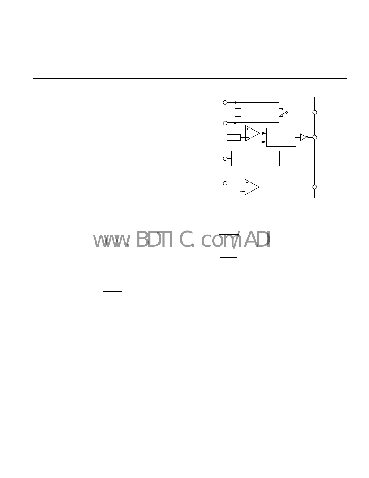
FUNCTIONAL BLOCK DIAGRAM
BATTERY
SWITCHOVER
CC
4.65V*
WATCHDOG
TRANSITION DETECTOR
(1.6s)
1.25V
*4.4V FOR ADM692A/ADM802M/ADM805M
( ) = ADM805L/M ONLY
RESET
GENERATOR
ADM690A
ADM692A
ADM802L
ADM802M
ADM805L
ADM805M
V
OUT
RESET
(RESET)
POWER FAIL
OUTPUT (PFO)
GENERAL DESCRIPTION
The ADM690A/ADM692A/ADM802L/M/ADM805L/M
family of supervisory circuits offers complete single chip
solutions for power supply monitoring and battery control
functions in microprocessor systems. These functions include
µP reset, backup battery switchover, watchdog timer, and power
failure warning.
The ADM690A/ADM692A/ADM802L/M/ADM805L/M are
available in 8-pin packages and provide:
1. Power-on reset output during power-up, power-down and
brownout conditions. The
RESET output remains opera-
tional with VCC as low as 1 V.
2. Battery backup switching for CMOS RAM, CMOS
microprocessor or other low power devices.
3. A reset pulse if the optional watchdog timer has not been
toggled within 1.6 seconds.
4. A 1.25 V threshold detector for power fail warning, low battery
detection, or to monitor a power supply other than +5 V.
On the ADM690A/ADM802L/ADM805L the reset voltage
threshold is 4.65 V. On the ADM692A/ADM802M/
ADM805M, the reset voltage threshold is 4.40 V.
The ADM802L/ADM802M guarantee power fail accuracies to
±2%.
The ADM805L/M provides an active high reset output, RESET
instead of
RESET.
The family of products is fabricated using an advanced epitaxial
CMOS process combining low power consumption and high
reliability.
RESET assertion is guaranteed with VCC as low as 1 V.
They provide a pin-compatible upgrade for the MAX690A/
MAX692A/MAX802L/MAX802M/MAX805L
All parts are available in 8-pin DIP and SOIC packages. The
ADM690A is also available in a new space-saving microSOIC
package.
REV. 0
Information furnished by Analog Devices is believed to be accurate and
reliable. However, no responsibility is assumed by Analog Devices for its
use, nor for any infringements of patents or other rights of third parties
which may result from its use. No license is granted by implication or
otherwise under any patent or patent rights of Analog Devices.
One Technology Way, P.O. Box 9106, Norwood, MA 02062-9106, U.S.A.
Tel: 617/329-4700 World Wide Web Site: http://www.analog.com
Fax: 617/326-8703 © Analog Devices, Inc., 1996
ADM690A/ADM692A/ADM802L/M/ADM805L/M–SPECIFICATIONS
www.BDTIC.com/ADI
(VCC = 4.75 V to 5.5 V (ADM690A/ADM802L/ADM805L), VCC = 4.5 V to 5.5 V, (ADM692A/ADM802M/ADM805M), V
unless otherwise noted)
Parameter Min Typ Max Units Test Conditions/Comments
V
CC/VBATT
OPERATION
1
VCC Operating Voltage Range 1.0 5.5 V
Supply Current (Excludes I
Supply Current in Battery Backup Mode 0.05 1.0 µAV
) 70 100 µA
OUT
CC
Battery Standby Current 5.5 V > V
(+ = Discharge, – = Charge) –0.1 +0.02 µA
V
Output Voltage VCC – 0.02 VCC – 0.01 V I
OUT
V
in Battery Backup Mode V
OUT
V
– 0.5 VCC – 0.05 V I
CC
BATT
– 0.05 V
V
– 0.02 V I
CC
– 0.002 V I
BATT
OUT
OUT
OUT
OUT
Battery Switchover Threshold 20 mV Power Up
–20 mV Power Down
Battery Switchover Hysteresis 40 mV
RESET THRESHOLD
Reset Voltage Threshold
ADM690A, ADM802L, ADM805L 4.5 4.65 4.75 V
ADM692A, ADM802M, ADM805M 4.25 4.4 4.5 V
ADM802L 4.55 4.7 V T
ADM802M 4.30 4.45 V T
A
A
Reset Threshold Hysteresis 40 mV
Reset Timeout Delay 140 200 280 ms
RESET Output Voltage VCC – 1.5 V I
0.4 V I
0.3 V I
RESET Output Voltage 0.8 V I
V
– 1.5 V ADM805L/M, I
CC
SOURCE
SINK
SINK
SOURCE
0.4 V ADM805L/M, I
WATCHDOG TIMER
Watchdog Timeout Period 1.0 1.6 2.25 s
WDI Input Pulse Width 50 ns V
IL
WDI Input Threshold
Logic Low 0.8 V
Logic High 3.5 V
WDI Input Current 10 µA WDI = V
–10 µA WDI = 0 V
= +2.8 V, TA = T
BATT
= 0 V, V
CC
BATT
> V
= 2.8 V
+ 0.2 V
BATT
= 5 mA
= 50 mA
= 250 mA
= 250 µA, V
= 25°C, V
= 25°C, V
CC
Falling
CC
Falling
CC
< V
= 800 µA
= 3.2 mA
= 100 µA, V
= 4 µA, V
= 1 V
CC
= 1.1 V
CC
SOURCE
= 3.2 mA
SINK
= 800 µA
= 0.4, VIH = 0.8 (VCC)
CC
MIN
BATT
to T
– 0.2 V
MAX
POWER FAIL DETECTOR
PFI Input Threshold 1.20 1.25 1.30 V ADM690A, ADM692A, ADM805L/M
1.225 1.25 1.275 V ADM802L/M
PFI Input Current –25 0.01 +25 nA
PFO Output Voltage VCC – 1.5 V I
NOTES
1
Either VCC or V
Specifications subject to change without notice.
can be 0 V if the other > +2.0 V.
BATT
–2–
0.4 V I
SOURCE
= 3.2 mA
SINK
= 800 µA
REV. 0
ADM690A/ADM692A/ADM802L/M/ADM805L/M
1
2
3
4
8
7
6
5
TOP VIEW
(Not to Scale)
ADM690A
ADM692A
ADM802L
ADM802M
ADM805L
ADM805M
PFO
WDI
RESET (RESET)
V
BATT
V
OUT
V
CC
GND
PFI
www.BDTIC.com/ADI
ABSOLUTE MAXIMUM RATINGS*
(TA = +25°C unless otherwise noted)
VCC . . . . . . . . . . . . . . . . . . . . . . . . . . . . . . . . . –0.3 V to +6 V
V
. . . . . . . . . . . . . . . . . . . . . . . . . . . . . . . –0.3 V to +6 V
BATT
All Other Inputs . . . . . . . . . . . . . . . . . .–0.3 V to VCC + 0.3 V
Input Current
VCC . . . . . . . . . . . . . . . . . . . . . . . . . . . . . . . . . . . . .200 mA
V
. . . . . . . . . . . . . . . . . . . . . . . . . . . . . . . . . . . 50 mA
BATT
GND . . . . . . . . . . . . . . . . . . . . . . . . . . . . . . . . . . . . 20 mA
Digital Output Current . . . . . . . . . . . . . . . . . . . . . . . . 20 mA
Power Dissipation, N-8 DIP . . . . . . . . . . . . . . . . . . . 400 mW
θJA Thermal Impedance . . . . . . . . . . . . . . . . . . . . 120°C/W
Power Dissipation, SO-8 SOIC . . . . . . . . . . . . . . . . . 500 mW
θJA Thermal Impedance . . . . . . . . . . . . . . . . . . . . 110°C/W
Operating Temperature Range
Industrial (A Version) . . . . . . . . . . . . . . . . –40°C to +85°C
Lead Temperature (Soldering, 10 sec) . . . . . . . . . . . .+300°C
Vapor Phase (60 sec) . . . . . . . . . . . . . . . . . . . . . . . .+215°C
Infrared (15 sec) . . . . . . . . . . . . . . . . . . . . . . . . . . . .+220°C
Storage Temperature Range . . . . . . . . . . . . –65°C to +150°C
ESD Rating . . . . . . . . . . . . . . . . . . . . . . . . . . . . . . . . . . >4 kV
*Stresses above those listed under “Absolute Maximum Ratings” may cause
permanent damage to the device. This is a stress rating only and functional
operation of the device at these or any other conditions above those listed in the
operational sections of this specification is not implied. Exposure to absolute
maximum ratings for extended periods of time may affect device reliability.
ORDERING GUIDE
Temperature Package
Model Range Option
ADM690AAN –40°C to +85°C N-8
ADM690AARN –40°C to +85°C SO-8
ADM690AARM –40°C to +85°C RM-8
ADM692AAN –40°C to +85°C N-8
ADM692AARN –40°C to +85°C SO-8
ADM802LAN –40°C to +85°C N-8
ADM802LARN –40°C to +85°C SO-8
ADM802MAN –40°C to +85°C N-8
ADM802MARN –40°C to +85°C SO-8
ADM805LAN –40°C to +85°C N-8
ADM805LARN –40°C to +85°C SO-8
ADM805MAN –40°C to +85°C N-8
ADM805MARN –40°C to +85°C SO-8
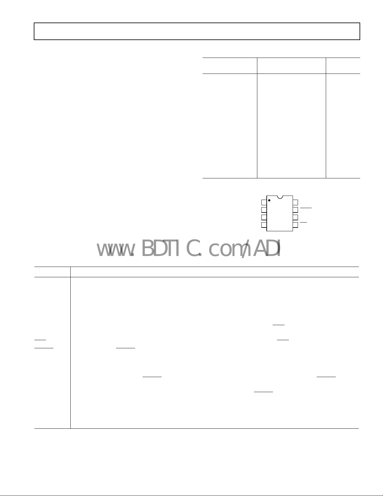
PIN CONFIGURATIONS
PIN FUNCTION DESCRIPTION
Mnemonic Function
V
V
V
CC
BATT
OUT
Power Supply Input: +5 V Nominal.
Backup Battery Input. As VCC falls below the reset threshold and below V
to V
Output Voltage. When VCC is above the reset threshold, V
When V
. On power-up as VCC rises to 20 mV above V
OUT
is below the reset threshold, the higher of VCC or V
CC
BATT
, V
will be switched back to VCC.
OUT
is connected to VCC through an on chip switch.
OUT
BATT
BATT
is connected to V
by 20 mV, V
.
OUT
will be switched
BATT
GND 0 V. Ground reference for all signals.
PFI Power Fail Comparator Input. If PFI is less than 1.25 V, the power fail output
should be connected to V
or GND.
CC
PFO goes low. If unused, PFI
PFO Power Fail Comparator Output. If PFI is less than 1.25 V, the power fail output PFO goes low.
RESET Logic Output. RESET goes low if
1. V
falls below the Reset Threshold
CC
2. The watchdog timer is not serviced within its timeout period (1.6 seconds)
The reset threshold is typically 4.65 V for the ADM690A/ADM802L/ADM805L and 4.4 V for the ADM692A/
ADM802M/ADM805M.
RESET remains low for 200 ms after VCC returns above the threshold. RESET also
goes low for 200 ms if the watchdog timer is enabled but not serviced within its timeout period.
RESET Active high RESET output (ADM805L/M only). This is the inverse of
or V
whichever is higher.
BATT
RESET. The asserted (high) level is V
CC
WDI Watchdog Input. WDI is a three level input. If WDI remains either high or low for longer than 1.6 s, (RESET)
(RESET) is activated. The timer resets with each transition on the WDI line. The watchdog timer may be
disabled if WDI is left floating or is connected to a high impedance three stated logic output.
REV. 0
–3–

ADM690A/ADM692A/ADM802L/M/ADM805L/M
www.BDTIC.com/ADI
Typical Performance Curves
3
2.75
R
= 9.3Ω
OUT
– V
2.5
OUT
V
2.25
2
10 7020 30 40 50 60
I
OUT
– mA
Figure 1. Output Voltage vs. Load Current in Battery
Backup
100
90
PFO
5.00
4.98
4.96
R
= 0.53Ω
I
OUT
OUT
– mA
4.88
– V
4.92
OUT
V
4.9
4.88
4.86
4.84
20 20050 100 150
Figure 4. Output Voltage vs. Load Current in Normal
Operation
TA = +258C
PFO
5V
100
90
10
1.3V
0%
PFI
1.2V
200mV
2µs
Figure 2. Power Fail Comparator Response Time L ➝ H
5V
100
90
V
CC
RESET
10
0%
1V
Figure 3. ADM690A
TA = +258C
RESET
Response Time
4V
10µs
1.3V
PFI
10
0%
200mV
2µs
0V
1.2V
Figure 5. Power Fail Comparator Response Time H ➝ L
100
90
10
0%
400ms1V
Figure 6.
RESET
Output Voltage vs. V
CC
–4–
REV. 0

V
+5V
0V
+5V
0V
+5V
0V
+5V
0V
0V
3.0V
3.0V
t
RS
V
CC
V
OUT
RESET
RESET
PFO
V
BATT
= PFI = 3.0V
www.BDTIC.com/ADI
BATT
V
ADM690A/ADM692A/ADM802L/M/ADM805L/M
BATTERY
SWITCHOVER
CC
V
OUT
WATCHDOG
INPUT (WDI)
4.65V*
WATCHDOG
TRANSITION DETECTOR
(1.6s)
RESET
GENERATOR
ADM690A
ADM692A
ADM802L
RESET
(RESET)
ADM802M
ADM805L
POWER FAIL
INPUT (PFI)
1.25V
*4.4V FOR ADM692A/ADM802M/ADM805M
( ) = ADM805L/M ONLY
ADM805M
POWER FAIL
OUTPUT (PFO)
Figure 7. Functional Block Diagram
POWER FAIL RESET, RESET
RESET is an active low output which provides a RESET signal
to the microprocessor whenever V
V
falls below the reset threshold, the RESET output is forced
CC
is at an invalid level. When
CC
low. The nominal reset voltage threshold is 4.65 V (ADM690A/
ADM802L/ADM805L or 4.4 V ADM692A/ADM802M/
ADM805M.
On power-up
RESET will remain low for 200 ms after VCC rises
above the reset threshold. This allows time for the power supply
and microprocessor to stabilize. On power-down, the
output remains low with V
as low as 1 V. This ensures that
CC
RESET
the microprocessor is held in a stable shutdown condition.
The guaranteed minimum and maximum thresholds are as follows:
ADM690A/ADM802L/ADM805L: 4.5 V and 4.75 V
ADM692A: 4.25 V and 4.5 V.
ADM802L: 4.55 V and 4.7 V
ADM802M: 4.3 V and 4.45 V
The ADM805L and ADM805M contain an active high reset
output. This is the complement of
RESET and is intended for
processors requiring an active high RESET signal.
The guaranteed minimum and maximum thresholds for the
ADM805 are:
ADM805L: 4.5 V and 4.75 V
ADM805M: 4.25 V and 4.5 V.
Watchdog Timer RESET, RESET
The watchdog timer circuit monitors the activity of the microprocessor in order to check that it is not stalled in an indefinite
loop. An output line on the processor is used to toggle the
Watchdog Input (WDI) line. If this line is not toggled within
1.6 seconds, a RESET pulse is generated. The watchdog
timeout period restarts with each transition on the WDI pin. To
ensure that the watchdog timer does not time out, either a
high-to-low or low-to-high transition on the WDI pin must
occur at or less than the minimum timeout period. If WDI
remains permanently either high or low, reset pulses will be
issued after each timeout period (1.6 s). The watchdog monitor
can be deactivated by floating the Watchdog Input (WDI) or by
connecting it to midsupply.
REV. 0
Figure 8. Timing Diagram
BATTERY SWITCHOVER SECTION
During normal operation with VCC higher than the reset
threshold, V
is internally switched to V
CC
via an internal
OUT
PMOS transistor switch. This switch has a typical on-resistance
of less than 1 Ω and can supply up to 100 mA at the V
OUT
terminal. Once VCC falls below the reset threshold, the higher of
V
or V
CC
connects to V
and V
is normally used to drive a RAM memory bank which
V
OUT
is switched to V
BATT
BATT
only when VCC is below the reset threshold
OUT
is greater than VCC.
. This means that V
OUT
BATT
may require instantaneous currents of greater than 100 mA. If
this is the case, then a bypass capacitor should be connected to
V
. The capacitor will provide the peak current transients to the
OUT
RAM. A capacitance value of 0.1 µF or greater may be used.
A 9 Ω MOSFET switch connects the V
input to V
BATT
OUT
during battery backup. This MOSFET has very low input-tooutput differential (dropout voltage) at the low current levels
required for battery backup of CMOS RAM or other low power
CMOS circuitry. The supply current in battery backup is
typically 0.05 µA.
Typically 3 V batteries are used as the backup supply. High
value capacitors, either standard electrolytic or the farad size
double layer capacitors, can also be used for short-term memory
back up. A small charging current of typically 10 nA (0.1 µA
max) flows out of the V
terminal. This current is useful for
BATT
maintaining rechargeable batteries in a fully charged condition.
This extends the life of the back up battery by compensating for
its self discharge current. Also note that this current poses no
problem when lithium batteries are used for back up since the
maximum charging current (0.1 µA) is safe for even the smallest
lithium cells.
If the battery-switchover section is not used, V
connected to GND and V
should be connected to VCC.
OUT
should be
BATT
–5–

ADM690A/ADM692A/ADM802L/M/ADM805L/M
1.25V
(PFO)
INPUT
POWER
R1
R2
PFI
R3
TO
µP NMI
5V
PFO
0V
0V V
L
V
H
V
IN
VH =
1.25 1
+ R
1
R2+R
3
R
2
×
R
3
VL = 1
.25+R1
1.25
VCC–
1.25
R
2
R
3
V
MID
=
1.25
R1+R
2
R
2
–
www.BDTIC.com/ADI
Table I. Input and Output Status in Battery Backup Mode
Signal Status
V
OUT
V
is connected to V
OUT
via an internal
BATT
PMOS switch.
RESET Logic low.
RESET Logic high (ADM805L, ADM805M). The open
circuit output voltage is equal to V
OUT
.
PFI The power fail comparator is disabled
PFO Logic low.
WDI The watchdog timer is disabled
Power Fail Comparator
The power fail comparator is an independent comparator
that may be used to monitor the input power supply. The
comparator’s inverting input is internally connected to a 1.25
V reference voltage. The noninverting input is available at the
PFI input. This input may be used to monitor the input power
supply via a resistive divider network. When the voltage on the
PFI input drops below 1.25 V, the comparator output (
PFO)
goes low indicating a power failure. For early warning of power
failure the comparator may be used to monitor the preregulator
input simply by choosing an appropriate resistive divider
network. The
PFO output can be used to interrupt the
processor so that a shutdown procedure is implemented before
the power is lost.
INPUT
POWER
R1
POWER
R2
FAIL
INPUT
1.25V
(PFO)
POWER FAIL
OUTPUT
Figure 9. Power Fail Comparator
Adding Hysteresis to the Power Fail Comparator
For increased noise immunity, hysteresis may be added to the
power fail comparator. Since the comparator circuit is noninverting, hysteresis can be added simply by connecting a
resistor between the
Figure 10. When
summing junction at the PFI pin. When
R3 sources current into the PFI summing junction. This results
in differing trip levels for the comparator. Further noise
PFO output and the PFI input as shown in
PFO is low, resistor R3 sinks current from the
PFO is high, resistor
immunity may be achieved by connecting a capacitor between
PFI and GND.
Figure 10. Adding Hysteresis to the Power Fail
Comparator
TYPICAL APPLICATIONS
Figure 11 shows a typical power monitoring, battery backup
application. V
operating conditions with V
connected to V
V
will be switched to V
OUT
the CMOS RAM. A
powers the CMOS RAM. Under normal
OUT
. If a power failure occurs, VCC will decay and
CC
present, V
CC
thereby maintaining power for
BATT
is internally
OUT
RESET pulse is also generated when V
CC
falls below the reset threshold.
UNREGULATED
DC
R1
R2
BATTERY
+5V
V
CC
V
GND
OUT
RESET
PFO
WDI
PFI
V
BATT
+
µP POWER
CMOS RAM
POWER
µP SYSTEM
µP RESET
µP NMI
I/O LINE
Figure 11. Typical Application Circuit
The watchdog timer input (WDI) monitors an I/O line from the
µP system. This line must be toggled once every 1.6 seconds to
verify correct software execution. Failure to toggle the line
indicates that the µP system is not correctly executing its
program and may be tied up in an endless loop. If this happens,
a reset pulse is generated to initialize the processor.
–6–
REV. 0

ADM690A/ADM692A/ADM802L/M/ADM805L/M
RESET
µP
V
CC
GND
+5V
RESET
GND
ADM690A
ADM692A
ADM802L
ADM802M
BUFFERED
RESET
www.BDTIC.com/ADI
If the watchdog timer is not needed, the WDI input should be
left floating.
The Power Fail Input, PFI, monitors the input power supply via
a resistive divider network. The voltage on the PFI input is
compared with a precision 1.25 V internal reference. If the input
voltage drops below 1.25 V, a power fail output (
PFO) signal is
generated. This warns of an impending power failure and may
be used to interrupt the processor so that the system may be
shut down in an orderly fashion. The resistors in the sensing
network are ratioed to give the desired power fail threshold
voltage V
.
T
= (1.25 R1/R2) + 1.25 V
V
T
R1/R2 = (V
/1.25) – 1
T
Alternate Watchdog Input Drive Circuits
The watchdog feature can be enabled and disabled under
program control by driving WDI with a 3-state buffer. When
three-stated, the WDI input will float thereby disabling the
watchdog timer.
High Capacity Backup Capacitors
High capacity (0.1 µF or greater) capacitors may be used as a
backup power source. A typical application is shown in Figure 12.
+5V
Operation Without a Backup Supply
If a backup power source is not used, V
nected to GND and V
should be connected to VCC.
OUT
should be con-
BATT
Replacing the Backup Battery
The backup battery may be replaced without any danger of
spurious resetting when V
reset threshold, a reset will not occur even if V
is present. Since VCC is above the
CC
is floating
BATT
while a replacement battery is being inserted. This differs from
older generation products where leakage currents flowing out
V
could cause spurious resetting during battery replacement.
BATT
mPs With Bidirectional RESET
In order to prevent contention for microprocessors with a
bidirectional reset line, a current limiting resistor should be
inserted between the ADM69xA/ADM80xx
RESET output pin
and the µP reset pin. This will limit the current to a safe level if
there are conflicting output reset levels. A suitable resistor value
is 4.7 kΩ. If the reset output is required for other uses, then it
should be buffered as shown in Figure 13.
V
RESET
RESET
GND
*
FOR ADM805L/ADM805M ONLY
OUT
*
TO STATIC RAM
TO µP
0.1F
V
CC
V
BATT
+
Figure 12. High Capacity Capacitor
Figure 13. Bidirectional Reset
REV. 0
–7–

ADM690A/ADM692A/ADM802L/M/ADM805L/M
www.BDTIC.com/ADI
OUTLINE DIMENSIONS
Dimensions shown in inches and (mm).
8-Pin Plastic DIP
(N-8)
0.430 (10.92)
0.348 (8.84)
0.210 (5.33)
MAX
0.160 (4.06)
0.115 (2.93)
0.022 (0.558)
0.014 (0.356)
8
14
0.1968 (5.00)
0.1890 (4.80)
PIN 1
0.100
(2.54)
BSC
0.070 (1.77)
0.045 (1.15)
5
0.280 (7.11)
0.240 (6.10)
0.060 (1.52)
0.015 (0.38)
0.130
(3.30)
MIN
SEATING
PLANE
8-Lead SOIC
(SO-8)
0.325 (8.25)
0.300 (7.62)
0.015 (0.381)
0.008 (0.204)
C2197–12–10/96
0.195 (4.95)
0.115 (2.93)
0.1574 (4.00)
0.1497 (3.80)
0.0098 (0.25)
0.0040 (0.10)
SEATING
PLANE
0.122 (3.10)
0.114 (2.90)
0.006 (0.15)
0.002 (0.05)
SEATING
PLANE
8
PIN 1
0.0500
(1.27)
BSC
0.122 (3.10)
0.114 (2.90)
8
1
PIN 1
0.0256 (0.65) BSC
0.120 (3.05)
0.112 (2.84)
0.018 (0.46)
0.008 (0.20)
5
0.2440 (6.20)
41
0.2284 (5.80)
0.0688 (1.75)
0.0532 (1.35)
0.0192 (0.49)
0.0138 (0.35)
0.0098 (0.25)
0.0075 (0.19)
8-Lead MicroSOIC
(RM-8)
5
0.199 (5.05)
0.187 (4.75)
4
0.043 (1.09)
0.037 (0.938)
0.011 (0.28)
0.003 (0.08)
0.0196 (0.50)
0.0099 (0.25)
8°
0°
0.0500 (1.27)
0.0160 (0.41)
0.120 (3.05)
0.112 (2.84)
33°
27°
x 45°
PRINTED IN U.S.A.
0.027 (0.68)
0.015 (0.38)
–8–
REV. 0
 Loading...