Analog Devices ADM805, ADM802, ADM690A, ADM692A Datasheet

Microprocessor
a
ADM690A/ADM692A/ADM802L/M/ADM805L/M
FEATURES
Precision Supply Voltage Monitor
4.65 V ADM690A/ADM802L/ADM805L
4.40 V ADM692A/ADM802M/ADM805M
Reset Assertion Down to 1 V V
Reset Timeout—200 ms
Watchdog Timer—1.6 s
100 mA Quiescent Supply Current
Automatic Battery Backup Power Switching
Voltage Monitor for Power Fail
62% Power Fail Accuracy on ADM802L/M
Space-Saving MicroSOIC Package (ADM690A)
APPLICATIONS
Microprocessor Systems
Computers
Controllers
Intelligent Instruments
CC
V
BATT
V
WATCHDOG
INPUT (WDI)
POWER FAIL
INPUT (PFI)
Supervisory Circuits
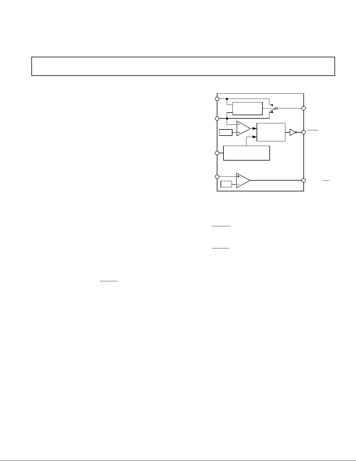
FUNCTIONAL BLOCK DIAGRAM
BATTERY
SWITCHOVER
CC
4.65V*
WATCHDOG
TRANSITION DETECTOR
(1.6s)
1.25V
*4.4V FOR ADM692A/ADM802M/ADM805M
( ) = ADM805L/M ONLY
RESET
GENERATOR
ADM690A
ADM692A
ADM802L
ADM802M
ADM805L
ADM805M
V
OUT
RESET
(RESET)
POWER FAIL
OUTPUT (PFO)
GENERAL DESCRIPTION
The ADM690A/ADM692A/ADM802L/M/ADM805L/M
family of supervisory circuits offers complete single chip
solutions for power supply monitoring and battery control
functions in microprocessor systems. These functions include
µP reset, backup battery switchover, watchdog timer, and power
failure warning.
The ADM690A/ADM692A/ADM802L/M/ADM805L/M are
available in 8-pin packages and provide:
1. Power-on reset output during power-up, power-down and
brownout conditions. The
RESET output remains opera-
tional with VCC as low as 1 V.
2. Battery backup switching for CMOS RAM, CMOS
microprocessor or other low power devices.
3. A reset pulse if the optional watchdog timer has not been
toggled within 1.6 seconds.
4. A 1.25 V threshold detector for power fail warning, low battery
detection, or to monitor a power supply other than +5 V.
On the ADM690A/ADM802L/ADM805L the reset voltage
threshold is 4.65 V. On the ADM692A/ADM802M/
ADM805M, the reset voltage threshold is 4.40 V.
The ADM802L/ADM802M guarantee power fail accuracies to
±2%.
The ADM805L/M provides an active high reset output, RESET
instead of
RESET.
The family of products is fabricated using an advanced epitaxial
CMOS process combining low power consumption and high
reliability.
RESET assertion is guaranteed with VCC as low as 1 V.
They provide a pin-compatible upgrade for the MAX690A/
MAX692A/MAX802L/MAX802M/MAX805L
All parts are available in 8-pin DIP and SOIC packages. The
ADM690A is also available in a new space-saving microSOIC
package.
REV. 0
Information furnished by Analog Devices is believed to be accurate and
reliable. However, no responsibility is assumed by Analog Devices for its
use, nor for any infringements of patents or other rights of third parties
which may result from its use. No license is granted by implication or
otherwise under any patent or patent rights of Analog Devices.
One Technology Way, P.O. Box 9106, Norwood, MA 02062-9106, U.S.A.
Tel: 617/329-4700 World Wide Web Site: http://www.analog.com
Fax: 617/326-8703 © Analog Devices, Inc., 1996

ADM690A/ADM692A/ADM802L/M/ADM805L/M–SPECIFICATIONS
(VCC = 4.75 V to 5.5 V (ADM690A/ADM802L/ADM805L), VCC = 4.5 V to 5.5 V, (ADM692A/ADM802M/ADM805M), V
unless otherwise noted)
Parameter Min Typ Max Units Test Conditions/Comments
V
CC/VBATT
OPERATION
1
VCC Operating Voltage Range 1.0 5.5 V
Supply Current (Excludes I
Supply Current in Battery Backup Mode 0.05 1.0 µAV
) 70 100 µA
OUT
CC
Battery Standby Current 5.5 V > V
(+ = Discharge, – = Charge) –0.1 +0.02 µA
V
Output Voltage VCC – 0.02 VCC – 0.01 V I
OUT
V
in Battery Backup Mode V
OUT
V
– 0.5 VCC – 0.05 V I
CC
BATT
– 0.05 V
V
– 0.02 V I
CC
– 0.002 V I
BATT
OUT
OUT
OUT
OUT
Battery Switchover Threshold 20 mV Power Up
–20 mV Power Down
Battery Switchover Hysteresis 40 mV
RESET THRESHOLD
Reset Voltage Threshold
ADM690A, ADM802L, ADM805L 4.5 4.65 4.75 V
ADM692A, ADM802M, ADM805M 4.25 4.4 4.5 V
ADM802L 4.55 4.7 V T
ADM802M 4.30 4.45 V T
A
A
Reset Threshold Hysteresis 40 mV
Reset Timeout Delay 140 200 280 ms
RESET Output Voltage VCC – 1.5 V I
0.4 V I
0.3 V I
RESET Output Voltage 0.8 V I
V
– 1.5 V ADM805L/M, I
CC
SOURCE
SINK
SINK
SOURCE
0.4 V ADM805L/M, I
WATCHDOG TIMER
Watchdog Timeout Period 1.0 1.6 2.25 s
WDI Input Pulse Width 50 ns V
IL
WDI Input Threshold
Logic Low 0.8 V
Logic High 3.5 V
WDI Input Current 10 µA WDI = V
–10 µA WDI = 0 V
= +2.8 V, TA = T
BATT
= 0 V, V
CC
BATT
> V
= 2.8 V
+ 0.2 V
BATT
= 5 mA
= 50 mA
= 250 mA
= 250 µA, V
= 25°C, V
= 25°C, V
CC
Falling
CC
Falling
CC
< V
= 800 µA
= 3.2 mA
= 100 µA, V
= 4 µA, V
= 1 V
CC
= 1.1 V
CC
SOURCE
= 3.2 mA
SINK
= 800 µA
= 0.4, VIH = 0.8 (VCC)
CC
MIN
BATT
to T
– 0.2 V
MAX
POWER FAIL DETECTOR
PFI Input Threshold 1.20 1.25 1.30 V ADM690A, ADM692A, ADM805L/M
1.225 1.25 1.275 V ADM802L/M
PFI Input Current –25 0.01 +25 nA
PFO Output Voltage VCC – 1.5 V I
0.4 V I
NOTES
1
Either VCC or V
Specifications subject to change without notice.
can be 0 V if the other > +2.0 V.
BATT
SOURCE
= 3.2 mA
SINK
= 800 µA
–2–
REV. 0

ADM690A/ADM692A/ADM802L/M/ADM805L/M
1
2
3
4
8
7
6
5
TOP VIEW
(Not to Scale)
ADM690A
ADM692A
ADM802L
ADM802M
ADM805L
ADM805M
PFO
WDI
RESET (RESET)
V
BATT
V
OUT
V
CC
GND
PFI
ABSOLUTE MAXIMUM RATINGS*
(TA = +25°C unless otherwise noted)
VCC . . . . . . . . . . . . . . . . . . . . . . . . . . . . . . . . . –0.3 V to +6 V
V
. . . . . . . . . . . . . . . . . . . . . . . . . . . . . . . –0.3 V to +6 V
BATT
All Other Inputs . . . . . . . . . . . . . . . . . .–0.3 V to VCC + 0.3 V
Input Current
VCC . . . . . . . . . . . . . . . . . . . . . . . . . . . . . . . . . . . . .200 mA
V
. . . . . . . . . . . . . . . . . . . . . . . . . . . . . . . . . . . 50 mA
BATT
GND . . . . . . . . . . . . . . . . . . . . . . . . . . . . . . . . . . . . 20 mA
Digital Output Current . . . . . . . . . . . . . . . . . . . . . . . . 20 mA
Power Dissipation, N-8 DIP . . . . . . . . . . . . . . . . . . . 400 mW
θJA Thermal Impedance . . . . . . . . . . . . . . . . . . . . 120°C/W
Power Dissipation, SO-8 SOIC . . . . . . . . . . . . . . . . . 500 mW
θJA Thermal Impedance . . . . . . . . . . . . . . . . . . . . 110°C/W
Operating Temperature Range
Industrial (A Version) . . . . . . . . . . . . . . . . –40°C to +85°C
Lead Temperature (Soldering, 10 sec) . . . . . . . . . . . .+300°C
Vapor Phase (60 sec) . . . . . . . . . . . . . . . . . . . . . . . .+215°C
Infrared (15 sec) . . . . . . . . . . . . . . . . . . . . . . . . . . . .+220°C
Storage Temperature Range . . . . . . . . . . . . –65°C to +150°C
ESD Rating . . . . . . . . . . . . . . . . . . . . . . . . . . . . . . . . . . >4 kV
*Stresses above those listed under “Absolute Maximum Ratings” may cause
permanent damage to the device. This is a stress rating only and functional
operation of the device at these or any other conditions above those listed in the
operational sections of this specification is not implied. Exposure to absolute
maximum ratings for extended periods of time may affect device reliability.
ORDERING GUIDE
Temperature Package
Model Range Option
ADM690AAN –40°C to +85°C N-8
ADM690AARN –40°C to +85°C SO-8
ADM690AARM –40°C to +85°C RM-8
ADM692AAN –40°C to +85°C N-8
ADM692AARN –40°C to +85°C SO-8
ADM802LAN –40°C to +85°C N-8
ADM802LARN –40°C to +85°C SO-8
ADM802MAN –40°C to +85°C N-8
ADM802MARN –40°C to +85°C SO-8
ADM805LAN –40°C to +85°C N-8
ADM805LARN –40°C to +85°C SO-8
ADM805MAN –40°C to +85°C N-8
ADM805MARN –40°C to +85°C SO-8
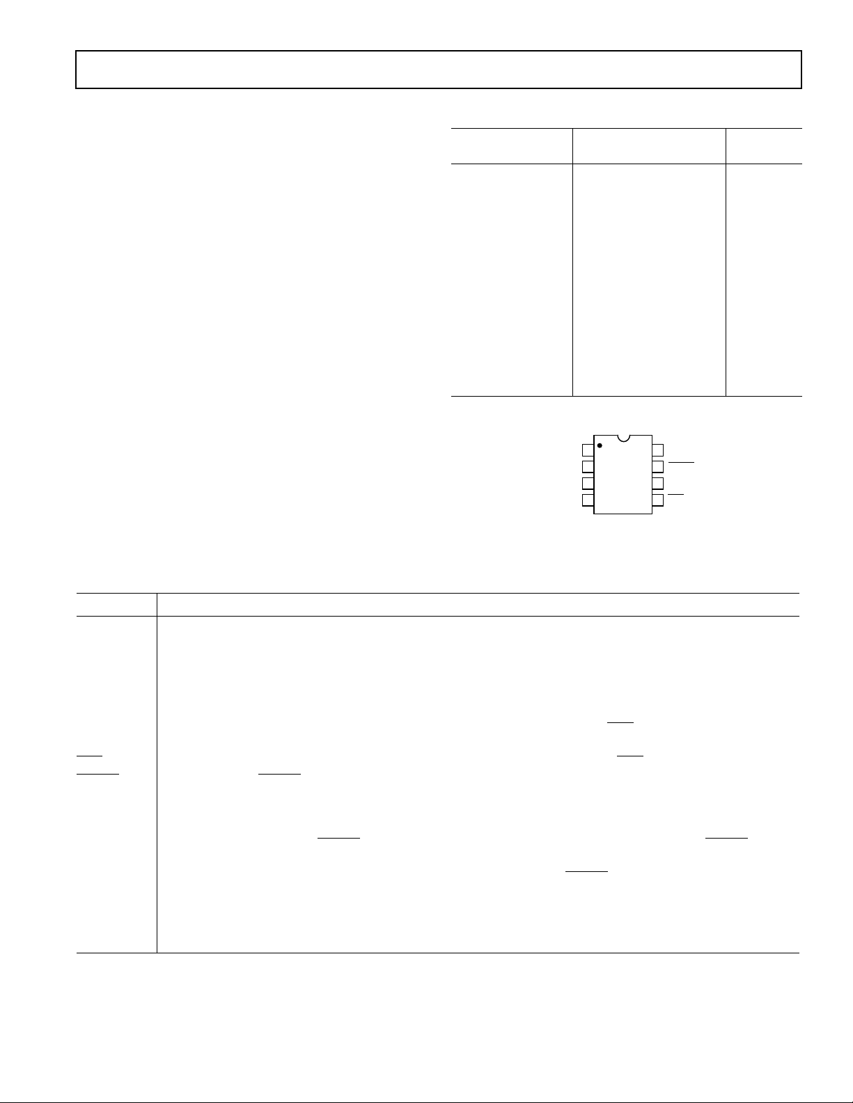
PIN CONFIGURATIONS
PIN FUNCTION DESCRIPTION
Mnemonic Function
V
V
V
CC
BATT
OUT
Power Supply Input: +5 V Nominal.
Backup Battery Input. As VCC falls below the reset threshold and below V
to V
Output Voltage. When VCC is above the reset threshold, V
When V
. On power-up as VCC rises to 20 mV above V
OUT
is below the reset threshold, the higher of VCC or V
CC
BATT
, V
will be switched back to VCC.
OUT
is connected to VCC through an on chip switch.
OUT
BATT
BATT
is connected to V
by 20 mV, V
.
OUT
will be switched
BATT
GND 0 V. Ground reference for all signals.
PFI Power Fail Comparator Input. If PFI is less than 1.25 V, the power fail output
should be connected to V
or GND.
CC
PFO goes low. If unused, PFI
PFO Power Fail Comparator Output. If PFI is less than 1.25 V, the power fail output PFO goes low.
RESET Logic Output. RESET goes low if
1. V
falls below the Reset Threshold
CC
2. The watchdog timer is not serviced within its timeout period (1.6 seconds)
The reset threshold is typically 4.65 V for the ADM690A/ADM802L/ADM805L and 4.4 V for the ADM692A/
ADM802M/ADM805M.
RESET remains low for 200 ms after VCC returns above the threshold. RESET also
goes low for 200 ms if the watchdog timer is enabled but not serviced within its timeout period.
RESET Active high RESET output (ADM805L/M only). This is the inverse of
or V
whichever is higher.
BATT
RESET. The asserted (high) level is V
CC
WDI Watchdog Input. WDI is a three level input. If WDI remains either high or low for longer than 1.6 s, (RESET)
(RESET) is activated. The timer resets with each transition on the WDI line. The watchdog timer may be
disabled if WDI is left floating or is connected to a high impedance three stated logic output.
REV. 0
–3–
 Loading...