

Datasheet ADM708ARM, ADM708AR, ADM708AN, ADM707ARM, ADM707AR Datasheet (Analog Devices)
...
Low Cost P
a
FEATURES
Guaranteed RESET Valid with V
190 A Quiescent Current
Precision Supply-Voltage Monitor
4.65 V (ADM705/ADM707)
4.40 V (ADM706/ADM708)
200 ms Reset Pulsewidth
Debounced TTL/CMOS Manual Reset Input (MR)
Independent Watchdog Timer—1.6 sec Timeout
(ADM705/ADM706)
Active High Reset Output (ADM707/ADM708)
Voltage Monitor for Power-Fail or Low Battery
Warning
Superior Upgrade for MAX705–MAX708
Also Available in MicroSOIC Packages
APPLICATIONS
Microprocessor Systems
Computers
Controllers
Intelligent Instruments
Critical P Monitoring
Automotive Systems
Critical P Power Monitoring
GENERAL DESCRIPTION
The ADM705–ADM708 are low cost µP supervisory circuits.
They are suitable for monitoring the 5 V power supply/battery
and can also monitor microprocessor activity.
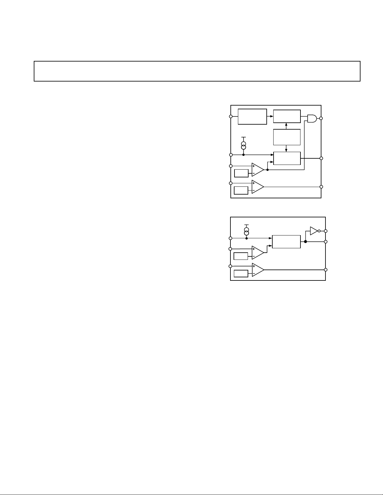
The ADM705/ADM706 provide the following functions:
1. Power-On Reset output during power-up, power-down and
brownout conditions. The RESET output remains operational with V
as low as 1 V.
CC
2. Independent watchdog timeout, WDO, that goes low if the
watchdog input has not been toggled within 1.6 seconds.
3. A 1.25 V threshold detector for power-fail warning, low
battery detection or to monitor a power supply other than
5V.
4. An active low debounced manual reset input (MR).
The ADM707/ADM708 differ in that:
1. A watchdog timer function is not available.
2. An active high reset output in addition to the active low
output is available.
= 1 V
CC
Supervisory Circuits
ADM705–ADM708
FUNCTIONAL BLOCK DIAGRAMS
WATCHDOG
INPUT (WDI)
MR
V
POWER-FAIL
INPUT (PFI)
MR
V
POWER-FAIL
INPUT (PFI)
Two supply-voltage monitor levels are available. The ADM705/
ADM707 generate a reset when the supply voltage falls below
4.65 V, while the ADM706/ADM708 require that the supply
fall below 4.40 V before a reset is issued.
All parts are available in 8-lead DIP and SOIC packages. The
ADM707 and ADM708 are also available in space-saving
microSOIC packages.
WATCHDOG
TRANSITION
DETECTOR
V
CC
250A
CC
4.65V*
1.25V
*VOLTAGE REFERENCE = 4.65V (ADM705), 4.40V (ADM706)
V
CC
250A
CC
4.65V*
1.25V
*VOLTAGE REFERENCE = 4.65V (ADM707), 4.40V (ADM708)
WATCHDOG
TIMER
RESET &
WATCHDOG
TIMEBASE
RESET
GENERATOR
ADM705/
ADM706
RESET
GENERATOR
ADM707/
ADM708
WATCHDOG
OUTPUT (WDO)
RESET
POWER-FAIL
OUTPUT (PFO)
RESET
RESET
POWER-FAIL
OUTPUT (PFO)
REV. B
Information furnished by Analog Devices is believed to be accurate and
reliable. However, no responsibility is assumed by Analog Devices for its
use, nor for any infringements of patents or other rights of third parties
which may result from its use. No license is granted by implication or
otherwise under any patent or patent rights of Analog Devices.
One Technology Way, P.O. Box 9106, Norwood, MA 02062-9106, U.S.A.
Tel: 781/329-4700 World Wide Web Site: http://www.analog.com
Fax: 781/326-8703 © Analog Devices, Inc., 2000

ADM705–ADM708–SPECIFICATIONS
(VCC = 4.75 V to 5.5 V, TA = T
MIN
to T
unless otherwise noted.)
MAX
Parameter Min Typ Max Unit Test Conditions/Comments
V
Operating Voltage Range 1.0 5.5 V
CC
Supply Current 190 250 µA
Reset Threshold 4.5 4.65 4.75 V ADM705, ADM707
4.25 4.40 4.50 V ADM706, ADM708
Reset Threshold Hysteresis 40 mV
Reset Pulsewidth 160 200 280 ms
RESET Output Voltage V
RESET Output Voltage V
Watchdog Timeout Period (t
WDI Pulsewidth (t
)50 nsV
WP
) 1.00 1.60 2.25 sec
WD
– 1.5 V I
CC
0.4 V I
0.3 V V
0.3 V V
– 1.5 V ADM707, ADM708, I
CC
0.4 V ADM707, ADM708, I
= 800 µA
SOURCE
= 3.2 mA
SINK
= 1 V, I
CC
= 1.2 V, I
CC
= 0.4 V, VIH = VCC × 0.8
IL
SINK
SINK
= 50 µA
= 100 µA
SOURCE
= 1.2 mA
SINK
= 800 µA
WDI Input Threshold
Logic Low 0.8 V
Logic High 3.5 V
WDI Input Current 50 150 µA WDI = V
CC
–150 –50 µA WDI = 0 V
WDO Output Voltage V
– 1.5 V I
CC
0.4 V I
SOURCE
= 1.2 mA
SINK
= 800 µA
MR Pull-Up Current 100 250 600 µA MR = 0 V
MR Pulsewidth 150 ns
MR Input Threshold 0.8 V
2.0 V
MR to Reset Output Delay 250 ns
PFI Input Threshold 1.2 1.25 1.3 V
PFI Input Current –25 0.01 25 nA
PFO Output Voltage V
Specifications subject to change without notice.
– 1.5 V I
CC
0.4 V I
SOURCE
= 3.2 mA
SINK
= 800 µA
ABSOLUTE MAXIMUM RATINGS*
(TA = 25°C unless otherwise noted)
VCC . . . . . . . . . . . . . . . . . . . . . . . . . . . . . . . . . . –0.3 V to +6 V
All Other Inputs . . . . . . . . . . . . . . . . . . –0.3 V to V
+ 0.3 V
CC
Input Current
V
. . . . . . . . . . . . . . . . . . . . . . . . . . . . . . . . . . . . . . 20 mA
CC
GND . . . . . . . . . . . . . . . . . . . . . . . . . . . . . . . . . . . . . 20 mA
Digital Output Current . . . . . . . . . . . . . . . . . . . . . . . . . 20 mA
Power Dissipation, N-8 DIP . . . . . . . . . . . . . . . . . . . . 727 mW
Thermal Impedance . . . . . . . . . . . . . . . . . . . . . 135°C/W
θ
JA
Power Dissipation, SO-8 SOIC . . . . . . . . . . . . . . . . . . 470 mW
θ
Thermal Impedance . . . . . . . . . . . . . . . . . . . . . 110°C/W
JA
Operating Temperature Range
Industrial (A Version) . . . . . . . . . . . . . . . . . –40°C to +85°C
Lead Temperature (Soldering, 10 sec) . . . . . . . . . . . . . 300°C
Vapor Phase (60 sec) . . . . . . . . . . . . . . . . . . . . . . . . . 215°C
Infrared (15 sec) . . . . . . . . . . . . . . . . . . . . . . . . . . . . . 220°C
Storage Temperature Range . . . . . . . . . . . . . –65°C to +150°C
ESD Rating . . . . . . . . . . . . . . . . . . . . . . . . . . . . . . . . . . .>5 kV
*Stresses above those listed under Absolute Maximum Ratings may cause perma-
nent damage to the device. This is a stress rating only; functional operation of the
device at these or any other conditions above those listed in the operational
sections of this specification is not implied. Exposure to absolute maximum
ratings for extended periods of time may affect device reliability
ORDERING GUIDE
Model Temperature Range Package Option
ADM705AN –40°C to +85°C N-8
ADM705AR –40°C to +85°C SO-8
ADM706AN –40°C to +85°C N-8
ADM706AR –40°C to +85°C SO-8
ADM707AN –40°C to +85°C N-8
ADM707AR –40°C to +85°C SO-8
ADM707ARM –40°C to +85°C RM-8
ADM708AN –40°C to +85°C N-8
ADM708AR –40°C to +85°C SO-8
ADM708ARM –40°C to +85°C RM-8
–2–
REV. B
ADM705–ADM708
PIN FUNCTION DESCRIPTION
Pin No.
ADM705 ADM707
ADM706 ADM708
Mnemonic DIP, SOIC DIP, SPOC MicroSOIC Function
MR 1 1 3 Manual Reset Input. When taken below 0.8 V, a RESET is gener-
ated. MR can be driven from TTL, CMOS logic or from a manual
reset switch as it is internally debounced. An internal 250 µA pull-up
current holds the input high when floating.
V
CC
GND 3 3 5 0 V. Ground reference for all signals.
PFI 4 4 6 Power-Fail Input. PFI is the noninverting input to the Power-Fail
PFO 5 5 7 Power-Fail Output. PFO is the output from the Power-Fail Compara-
WDI 6 N/A N/A Watchdog Input. WDI is a three-level input. If WDI remains either
NC N/A 6 8 No Connect.
RESET 7 7 1 Logic Output. RESET goes low for 200 ms when triggered. It can be
WDO 8 N/A N/A Logic Output. The Watchdog Output, WDO, goes low if the internal
RESET N/A 8 2 Logic Output. RESET is an active high output suitable for systems
2 2 4 5 V Power Supply Input.
Comparator. When PFI is less than 1.25 V, PFO goes low. If unused,
PFI should be connected to GND or V
tor. It goes low when PFI is less than 1.25 V.
high or low for longer than the watchdog timeout period, the watchdog output WDO goes low. The timer resets with each transition at
the WDI input.
Either a high-to-low or a low-to-high transition will clear the counter.
The internal timer is also cleared whenever reset is asserted. The
watchdog timer is disabled when WDI is left floating or connected to
a three-state buffer.
triggered either by V
being below the reset threshold or by a low
CC
signal on the manual reset (MR) input. RESET will remain low
whenever V
is below the reset threshold (4.65 V in ADM705, 4.4 V
CC
in ADM706). It remains low for 200 ms after V
reset threshold or MR goes from low to high. A watchdog timeout
will not trigger RESET unless WDO is connected to MR.
watchdog timer times out as a result of inactivity on the WDI input. It
remains low until the watchdog timer is cleared. WDO also goes low
during low line conditions. Whenever V
WDO remains low. As soon as V
WDO goes high immediately.
that use active high RESET logic. It is the inverse of RESET.
.
CC
goes above the
CC
is below the reset threshold,
CC
goes above the reset threshold,
CC
REV. B
PIN CONFIGURATION
DIP, SOIC DIP, SOIC MicroSOIC
1
MR
V
GND
PFI
CC
1
ADM705/
2
3
(Not to Scale)
4
ADM706
TOP VIEW
8
7
6
5
WDO
RESET
WDI
PFO
1
MR
2
V
CC
3
GND
(Not to Scale)
4
PFI
NC = NO CONNECT
ADM707/
ADM708
TOP VIEW
8
7
6
5
RESET
RESET
NC
PFO
RESET
2
RESET
3
MR
V
4
CC
NC = NO CONNECT
ADM707/
ADM708
TOP VIEW
(Not to Scale)
–3–
8
NC
PFO
7
6
PFI
GND
5

ADM705–ADM708
(
)
WATCHDOG
INPUT (WDI)
MR
V
POWER-FAIL
INPUT (PFI)
WATCHDOG
TRANSITION
DETECTOR
V
CC
250A
CC
4.65V*
1.25V
*VOLTAGE REFERENCE = 4.65V (ADM705), 4.40V (ADM706)
WATCHDOG
TIMER
RESET &
WATCHDOG
TIMEBASE
RESET
GENERATOR
ADM705/
ADM706
WATCHDOG
OUTPUT (WDO)
RESET
POWER-FAIL
OUTPUT (PFO)
Figure 1. ADM705/ADM706 Functional Block Diagram
V
CC
MR
V
POWER-FAIL
INPUT (PFI)
250A
GENERATOR
CC
4.65V*
1.25V
*VOLTAGE REFERENCE = 4.65V
RESET
ADM707/
ADM708
ADM707), 4.40V (ADM708
RESET
RESET
POWER-FAIL
OUTPUT (PFO)
Figure 2. ADM707/ADM708 Functional Block Diagram
CIRCUIT INFORMATION
Power-Fail RESET Output
RESET is an active low output that provides a RESET signal to
the Microprocessor whenever the V
input is below the reset
CC
threshold. An internal timer holds RESET low for 200 ms after
the voltage on V
rises above the threshold. This is intended as
CC
a power-on RESET signal for the microprocessor. It allows time
for both the power supply and the microprocessor to stabilize
after power-up. The RESET output is guaranteed to remain
valid (low) with V
as low as 1 V. This ensures that the micro-
CC
processor is held in a stable shutdown condition as the power
supply voltage ramps up.
In addition to RESET, an active high RESET output is also
available on the ADM707/ADM708. This is the complement of
RESET and is useful for processors requiring an active high
RESET signal.
Manual Reset (ADM707/ADM708)
The manual reset input (MR) allows other reset sources, such as
a manual reset switch, to generate a processor reset. The input
is effectively debounced by the timeout period (200 ms typical).
The MR input is TTL/CMOS compatible, so it may also be
driven by any logic reset output.
V
RESET
MR
WDO
CC
VRT VRT
Figure 3.
RESET, MR
t
RS
, and
WDO
MR EXTERNALLY
DRIVEN LOW
Timing
t
RS
Watchdog Timer (ADM705/ADM706)
The watchdog timer circuit may be used to monitor the activity
of the microprocessor in order to check that it is not stalled in an
indefinite loop. An output line on the processor is used to toggle
the Watchdog Input (WDI) line. If this line is not toggled
within the timeout period (1.6 sec), the watchdog output
(WDO) goes low. The WDO output may be connected to a
nonmaskable interrupt (NMI) on the processor; therefore, if the
watchdog timer times out, an interrupt is generated. The interrupt service routine should then be used to rectify the problem.
If a RESET signal is required when a timeout occurs, the WDO
output should be connected to the manual reset input (MR).
The watchdog timer is cleared by either a high-to-low or by a
low-to-high transition on WDI. It is also cleared by RESET
going low; therefore, the watchdog timeout period begins after
RESET goes high.
When V
falls below the reset threshold, WDO is forced low
CC
whether or not the watchdog timer has timed out. Normally,
this would generate an interrupt, but it is overridden by RESET
going low.
The watchdog monitor can be deactivated by floating the
Watchdog Input (WDI). The WDO output can now be used as
a low-line output since it will only go low when V
falls below
CC
the reset threshold.
WDI
t
WP
t
WD
t
WD
t
WD
WDO
RESET
RESET EXTERNALLY
TRIGGERED BY MR
t
RS
Figure 4. Watchdog Timing
–4–
REV. B

Power-Fail Comparator
The power-fail comparator is an independent comparator that
may be used to monitor the input power supply. The comparator’s
inverting input is internally connected to a 1.25 V reference
voltage. The noninverting input is available at the PFI input.
This input may be used to monitor the input power supply via
a resistive divider network. When the voltage on the PFI input
drops below 1.25 V, the comparator output (PFO) goes low,
indicating a power failure. For early warning of power failure,
the comparator may be used to monitor the preregulator input
simply by choosing an appropriate resistive divider network.
The PFO output can be used to interrupt the processor so that
a shutdown procedure is implemented before the power is lost.
INPUT
POWER
R1
R2
POWER-FAIL
INPUT
1.25V
PFI
ADM70x
PFO
POWER-FAIL
OUTPUT
ADM705–ADM708
[
.
RR
+
RR
125
12
RR
R
CC
.]
1251
V
=
H
.
=+
125 1
VR
L
MID
125
=
V
Valid RESET Below 1 V V
The ADM70x family of products is guaranteed to provide a
valid reset level with V
as low as 1 V; please refer to the Typi-
CC
cal Performance Characteristics. As V
internal transistor will not have sufficient drive to hold it ON so
the voltage on RESET will no longer be held at 0 V. A pull-down
resistor as shown in Figure 7 may be connected externally to
hold the line low if it is required.
23
+
23
×
.
V
CC
–
2
R
+
2
CC
1
R
– .
125
RE
drops below 1 V, the
Figure 5. Power-Fail Comparator
Adding Hysteresis to the Power-Fail Comparator
For increased noise immunity, hysteresis may be added to the
power-fail comparator. Since the comparator circuit is noninverting, hysteresis can be added simply by connecting a
resistor between the PFO output and the PFI input as shown in
Figure 6. When PFO is low, resistor R3 sinks current from the
summing junction at the PFI pin. When PFO is high, resistor
R3 sources current into the PFI summing junction. This results
in differing trip levels for the comparator. Further noise immunity may be achieved by connecting a capacitor between PFI
and GND.
7V TO 15V
INPUT POWER
ADM663
R1
R2
5V
PFO
5V
1.25V
PFI
V
CC
ADM70x
PFO
R3
TO P NMI
Figure 7.
ADM70x
RESET
GND
RESET
R1
Valid Below 1 V
0V
0V
V
H
V
L
V
IN
Figure 6. Adding Hysteresis to the Power-Fail Comparator
REV. B
–5–

ADM705–ADM708–Typical Performance Characteristics
V
= 5V
CC
= 25ⴗC
TA
1.2V
PFO
0V
V
RESET
4.50VA!
100
CC
90
10
0%
1V
1V
500msH
o
1.3V
PFI
4.4V
500ns/DIV
Figure 8.
V
RESET
RESET
100
CC
90
10
0%
Output Voltage vs. Supply Voltage
4.50VA1
1V
1V
500msH
o
Figure 9. ADM707/ADM708 RESET Output Voltage vs.
Supply Voltage
V
= 5V
CC
= 25ⴗC
T
A
1.3V
PFI
1.2V
Figure 11. PFI Comparator Deassertion Response Time
V
= V
CC
5V
0V
5V
RT
TA = 25ⴗC
RESET
Figure 12.
RESET
100ns/DIV
RESET
RESET
, RESET Assertion
V
= V
CC
RT
TA = 25ⴗC
RESET
5V
0V
5V
5V
PFO
0V
500ns/DIV
Figure 10. PFI Comparator Assertion Response Time
0V
Figure 13.
100ns/DIV
RESET
, RESET Deassertion
0V
REV. B–6–

ADM705–ADM708
5V
V
CC
5V
RESET
2s/DIV
Figure 14. ADM705/ADM707
TA = 25ⴗC
RESET
Response Time
4V
0V
APPLICATIONS
A Typical Operating Circuit is shown in Figure 15. The unregulated dc input supply is monitored using the PFI input via the
resistive divider network. Resistors R1 and R2 should be selected
so that when the supply voltage drops below the desired level
(e.g., 8 V), the voltage on PFI drops below the 1.25 V threshold
thereby generating an interrupt to the µP. Monitoring the pre-
regulator input gives additional time to execute an orderly
shutdown procedure before power is lost.
UNREGULATED
DC
R1
R2
ADM666
GNDIN OUT
V
CC
ADM705/
ADM706
PFI
MR
MANUAL
RESET
GND
RESET
WDI
WDO
PFO
5V
P
V
CC
RESET
I/O LINE
NMI
INTERRUPT
If, in the event of inactivity on the WDI line, a system reset is
required, then the WDO output should be connected to the MR
input as shown in Figure 16.
RESET
ADM705/
ADM706
MR
WDO
GND
Figure 16.
WDI
RESET
RESET
I/O LINE
from
P
WDO
Monitoring Additional Supply Levels
It is possible to use the power-fail comparator to monitor a
second supply as shown in Figure 17. The two sensing resistors,
R1 and R2, are selected so that the voltage on PFI drops below
1.25 V at the minimum acceptable input supply. The PFO
output may be connected to the MR input so that a RESET is
generated when the supply drops out of tolerance. In this case, if
either supply drops out of tolerance, a RESET will be generated.
ADM705/
ADM706
PFI
MR
GND
5V
V
CC
RESET
PFO
RESET
P
X
V
X
R1
R2
Figure 17. Monitoring 5 V and an Additional Supply, V
Ps With Bidirectional RESET
In order to prevent contention for microprocessors with a bidirectional reset line, a current limiting resistor should be inserted
between the ADM70x RESET output pin and the µP reset pin.
This will limit the current to a safe level if there are conflicting
output reset levels. A suitable resistor value is 4.7 kΩ. If the
reset output is required for other uses, it should be buffered as
shown in Figure 18.
Figure 15. Typical Application Circuit
Microprocessor activity is monitored using the WDI input. This
is driven using an output line from the processor. The software
routines should toggle this line at least once every 1.6 seconds.
If a problem occurs and this line is not toggled, WDO goes low
and a nonmaskable interrupt is generated. This interrupt routine may be used to clear the problem.
REV. B
–7–
5V
V
CC
ADM70x
RESET
GND
RESET
Figure 18. Bidirectional I-O
BUFFERED
RESET
P
GND
RESET

ADM705–ADM708
0.165 ± 0.01
(4.19 ± 0.25)
0.125 (3.18)
MIN
0.018 ± 0.003
(0.46 ± 0.08)
0.1574 (4.00)
0.1497 (3.80)
OUTLINE DIMENSIONS
Dimensions shown in inches and (mm).
8-Lead Plastic DIP
(N-8)
0.39 (9.91)
MAX
8
14
0.10 (2.54)
PIN 1
TYP
5
0.033
(0.84)
NOM
0.25
0.31
(6.35)
(7.87)
0.035 ± 0.01
(0.89 ± 0.25)
0.18 ± 0.03
(4.57 ± 0.76)
SEATING
PLANE
0.30 (7.62)
0° - 15°
8-Lead SOIC
(SO-8)
0.1968 (5.00)
0.1890 (4.80)
8
5
0.2440 (6.20)
41
0.2284 (5.80)
REF
0.011 ± 0.003
(4.57 ± 0.76)
C00088a–0–8/00 (rev. B)
0.0098 (0.25)
0.0040 (0.10)
SEATING
PLANE
0.122 (3.10)
0.114 (2.90)
0.006 (0.15)
0.002 (0.05)
SEATING
PLANE
PIN 1
0.0500
(1.27)
BSC
0.122 (3.10)
0.114 (2.90)
85
1
PIN 1
0.0256 (0.65) BSC
0.120 (3.05)
0.112 (2.84)
0.018 (0.46)
0.008 (0.20)
0.0688 (1.75)
0.0532 (1.35)
0.0192 (0.49)
0.0138 (0.35)
0.0098 (0.25)
0.0075 (0.19)
8-Lead MicroSOIC
(RM-8)
0.199 (5.05)
0.187 (4.75)
4
0.043 (1.09)
0.027 (0.68)
0.011 (0.28)
0.003 (0.08)
0.0196 (0.50)
0.0099 (0.25)
8°
0°
0.0500 (1.27)
0.0160 (0.41)
0.120 (3.05)
0.112 (2.84)
33°
27°
x 45°
0.027 (0.68)
0.015 (0.38)
PRINTED IN U.S.A.
–8–
REV. B
 Loading...