

Microprocessor Supervisory
V
www.BDTIC.com/ADI
FEATURES
Specified over temperature
Low power consumption (12 μA)
Precision monitoring of 2.5 V, 3 V, 3.3 V,
and 5
V power supply voltages
Reset timeout period of 140 ms (minimum)
Manual reset input
Output stages
Push-pull
Open-drain
Reset assertion down to 1 V V
Power supply glitch immunity
4-lead SC70 package
APPLICATIONS
Microprocessor systems
Computers
Controllers
Intelligent instruments
Automotive systems
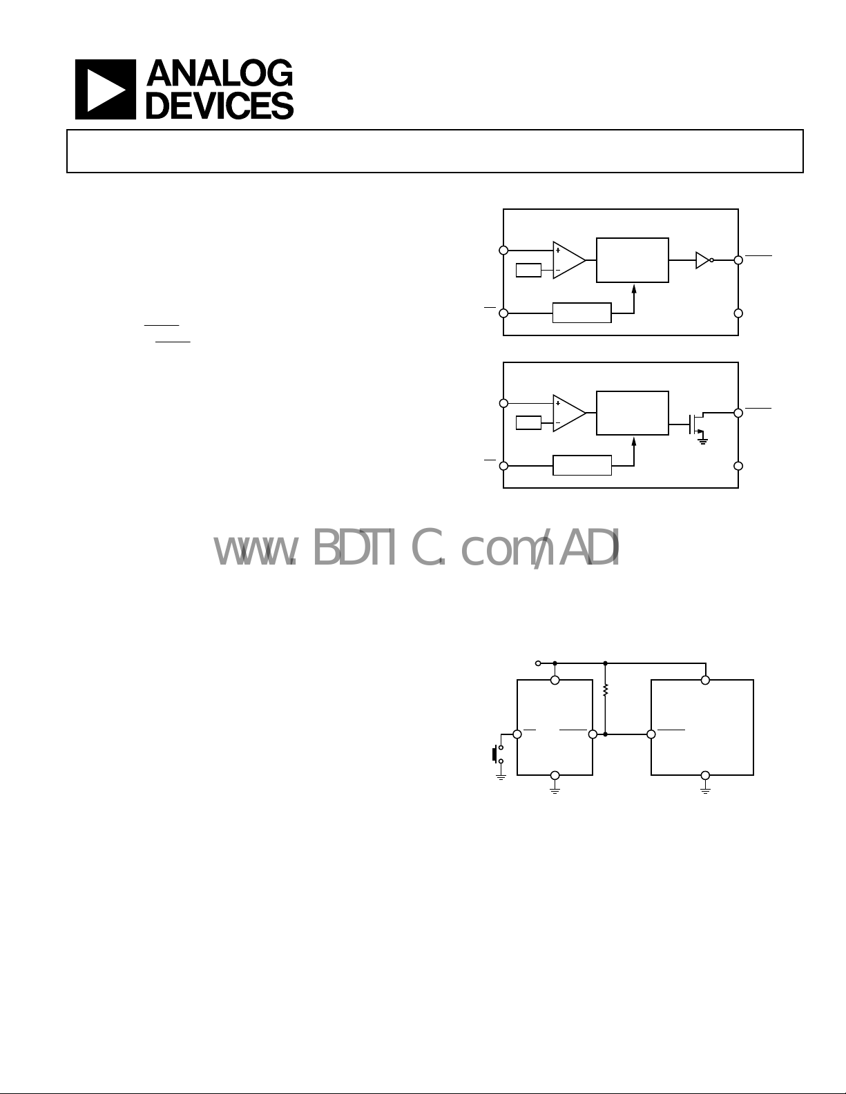
GENERAL DESCRIPTION
The ADM6711/ADM6713 are reset generator circuits suitable
for use in microprocessor-based systems. They provide a reset
signal on power-up, power-down, and whenever the supply
voltage falls below a preset threshold. In addition, both parts
have a debounced manual reset input so that a reset signal can
also be initiated with an external switch or logic signal.
With six different reset threshold options available ranging
from 2.32 V to 4.63 V, the ADM6711/ADM6713 are suitable for
monitoring 2.5 V, 3 V, 3.3 V, and 5 V supplies. A reset timeout
of at least 140 ms occurs when V
This gives the supply voltage time to stabilize before the
microprocessor starts up.
The ADM6711 has a push-pull output, so no additional
ernal components are needed. The ADM6713 open-drain
ext
output requires an external pull-up resistor that can be
connected to a voltage higher than V
output (ADM6711)
RESET
output (ADM6713)
RESET
CC
rises above the threshold.
CC
, if desired.
CC
Circuit in 4-Lead SC70
ADM6711/ADM6713
FUNCTIONAL BLOCK DIAGRAMS
ADM6711
CC
V
REF
MR
V
CC
MR
ADM6713
V
REF
DEBOUNCE
DEBOUNCE
The parts are highly reliable with accurate voltage references
a
nd immunity to fast, negative-going transients on V
current consumption and space-efficient, 4-lead SC70
packaging make the ADM6711/ADM6713 ideal for use in low
power portable applications.
V
CC
ADM6711/
ADM6713
RESET RESETMR
GND GND
Figure 3. Typical Operating Circuit
RESET
GENERATOR
240ms
Figure 1.
RESET
GENERATOR
240ms
Figure 2.
*R
PULL-UP
*ADM6713 ON LY
CC
V
MICROPROCESSOR
CC
SYSTEM
RESET
GND
RESET
GND
. Low
03754-002
3754-011
03754-001
Rev. A
Information furnished by Analog Devices is believed to be accurate and reliable. However, no
responsibility is assumed by Anal og Devices for its use, nor for any infringements of patents or ot her
rights of third parties that may result from its use. Specifications subject to change without notice. No
license is granted by implication or otherwise under any patent or patent rights of Analog Devices.
Trademarks and registered trademarks are the property of their respective owners.
One Technology Way, P.O. Box 9106, Norwood, MA 02062-9106, U.S.A.
Tel: 781.329.4700 www.analog.com
Fax: 781.461.3113 ©2006 Analog Devices, Inc. All rights reserved.

ADM6711/ADM6713
www.BDTIC.com/ADI
TABLE OF CONTENTS
Features .............................................................................................. 1
Applications....................................................................................... 1
Functional Block Diagrams............................................................. 1
General Description......................................................................... 1
Revision History ............................................................................... 2
Specifications..................................................................................... 3
Absolute Maximum Ratings............................................................ 5
ESD Caution.................................................................................. 5
Pin Configuration and Function Descriptions............................. 6
REVISION HISTORY
12/06—Rev. 0 to Rev. A
Updated Format..................................................................Universal
Changes to Specifications Table...................................................... 3
Changes to Figure 10........................................................................ 8
Changes to Ordering Guide............................................................ 9
8/03—Revision 0: Initial Version
Typical Perf or m an c e Charac t e r istics ..............................................7
Circuit Description............................................................................8
Manual Reset Input .......................................................................8
Power Supply Glitch Immunity ...................................................8
ADM6713
Ensuring a Valid
Outline Dimensions ..........................................................................9
Ordering Guide .............................................................................9
Output Logic Levels.....................................8
RESET
Output Down To V
RESET
CC
= 0 V ............8
Rev. A | Page 2 of 12
ADM6711/ADM6713
www.BDTIC.com/ADI
SPECIFICATIONS
VCC = full operating range; TA = T
unless otherwise noted.
Table 1.
Parameter Min Typ Max Unit Test Conditions/Comments
SUPPLY
VCC Operating Voltage Range 1.0 5.5 V TA = 0°C to 70°C
1.2 5.5 V TA = −40°C to +125°C
Supply Current 16 35 A VCC < 5.5 V, ADM671_L/M,
T
12 30 A VCC < 3.6 V, ADM671_R/S/T/Z,
T
60 A VCC < 5.5 V, ADM671_L/M,
T
60 A VCC < 3.6 V, ADM671_R/S/T/Z,
T
RESET VOLTAGE THRESHOLD
ADM671_L 4.56 4.63 4.70 V TA = 25°C
4.50 4.75 V TA = −40°C to +85°C
4.44 4.82 V TA = 85°C to 125°C
ADM671_M 4.31 4.38 4.45 V TA = 25°C
4.25 4.50 V TA = −40°C to +85°C
4.20 4.56 V TA = 85°C to 125°C
ADM671_T 3.04 3.08 3.11 V TA = 25°C
3.00 3.15 V TA = −40°C to +85°C
2.95 3.21 V TA = 85°C to 125°C
ADM671_S 2.89 2.93 2.96 V TA = 25°C
2.85 3.00 V TA = −40°C to +85°C
2.81 3.05 V TA = 85°C to 125°C
ADM671_R 2.59 2.63 2.66 V TA = 25°C
2.55 2.70 V TA = −40°C to +85°C
2.52 2.74 V TA = 85°C to 125°C
ADM671_Z 2.28 2.32 2.35 V TA = 25°C
2.25 2.38 V TA = −40°C to +85°C
2.22 2.42 V TA = 85°C to 125°C
RESET THRESHOLD TEMPERATURE
COEFFICIENT
VCC to RESET DELAY
RESET ACTIVE TIMEOUT PERIOD
100 640 ms TA = 85°C to 125°C
RESET OUTPUT VOLTAGE
Low (ADM6711/ADM6713) 0.3 V VCC = VTH min, I
ADM671_R/S/T/Z
0.4 V VCC = VTH min, I
ADM671_L/M
0.3 V VCC >1.0 V, I
High (ADM6711) 0.8 V
ADM6711R/S/T/Z
0.8 V
ADM6711L/M
to T
MIN
; VCC typ = 5 V for L/M models, 3.3 V for T/S models, 3 V for R models, and 2.5 V for Z models,
MAX
30 ppm/°C
20 s V
140 240 460 ms T
CC
CC
V VCC > VTH max, I
V VCC > VTH max, I
= −40°C to +85°C
A
= −40°C to +85°C
A
= 85°C to 125°C
A
= 85°C to 125°C
A
= VTH to (VTH − 100 mV)
CC
= −40°C to +85°C
A
= 1.2 mA,
SINK
= 3.2 mA,
SINK
= 50 A
SINK
SOURCE
SOURCE
= 500 A,
= 800 A,
Rev. A | Page 3 of 12
ADM6711/ADM6713
www.BDTIC.com/ADI
Parameter Min Typ Max Unit Test Conditions/Comments
RESET OPEN-DRAIN OUTPUT
LEAKAGE CURRENT
MANUAL RESET (MR)
Input Threshold 0.3 V
0.7 V
Pull-Up Resistance 10 20 kΩ
Minimum Pulse width 1 µs
Glitch Immunity 100 ns
Reset Delay 200 ns
1 µA
CC
V V
CC
V VIH
> VTH, RESET deasserted
V
CC
IL
Rev. A | Page 4 of 12

ADM6711/ADM6713
www.BDTIC.com/ADI
ABSOLUTE MAXIMUM RATINGS
TA = 25°C, unless otherwise noted.
Table 2.
Parameter Rating
V
CC
RESET (Push-Pull)
RESET (Open-Drain)
MR
Input Current
VCC, MR
Output Current
RESET
Rate of Rise, VCC 100 V/µs
θJA Thermal Impedance, SC70 146°C/W
Operating Temperature Range −40°C to +125°C
Storage Temperature Range −65°C to +150°C
Lead Temperature (Soldering, 10 sec) 300°C
Stresses above those listed under Absolute Maximum Ratings
ma
y cause permanent damage to the device. This is a stress
rating only; functional operation of the device at these or any
other conditions above those indicated in the operational
section of this specification is not implied. Exposure to absolute
maximum rating conditions for extended periods may affect
device reliability.
−0.3 V to +6 V
−0.3 V to ( V
−0.3 V to +6 V
−0.3 V to ( V
20 mA
20 mA
CC
CC
+ 0.3 V)
+ 0.3 V)
Table 3.
Model
ADM671_L 4.63
ADM671_M 4.38
ADM671_T 3.08
ADM671_S 2.93
ADM671_R 2.63
ADM671_Z 2.32
Threshold Options
RESET
RESET
ESD CAUTION
Threshold (V)
Rev. A | Page 5 of 12

ADM6711/ADM6713
www.BDTIC.com/ADI
PIN CONFIGURATION AND FUNCTION DESCRIPTIONS
1
GND
ADM6711/
ADM6713
TOP VIEW
(Not to Scale)
2
RESET
Figure 4. Pin Configuration
Table 4. Pin Function Descriptions
Pin No. Mnemonic Description
1 GND Ground Reference for All Signals (0 V).
2
3
RESET
MR
Active Low Logic Input. RESET remains low while VCC is below the reset threshold and remains low for
240 ms (typical) after V
rises above the reset threshold.
CC
Manual Reset. This active low debounced input ignores input pulses of 100 ns (typical) and is guaranteed
to accept input pulses greater than 1 µs. Leave floating when not used.
4 V
CC
Supply Voltage Being Monitored.
V
4
CC
3
MR
03754-003
Rev. A | Page 6 of 12

ADM6711/ADM6713
www.BDTIC.com/ADI
TYPICAL PERFORMANCE CHARACTERISTICS
12
10
8
(µA)
6
DD
I
4
2
0
–40 –20 0 20 5030 70 85 100 120
IDD @ VCC = 5.5V
IDD @ VCC = 3V
IDD @ VCC = 1V
TEMPERATURE (° C)
Figure 5. Supply Current vs. Temperature
1000
900
800
700
600
500
400
300
200
POWER-DOWN RESET DELAY (µs)
100
0
–40 –20 0 20 5030 70 85 100 120
Figure 6. Power-Down
900
800
700
600
500
400
300
200
POWER-DOWN RESET DELAY (µs)
100
0
–40
Figure 7. Power-Down
VOD = 20mV
VOD = 125mV
VOD = 200mV
TEMPERATURE (°C)
RESET
Delay vs. Temperature: ADM671_R/S/T/Z
VOD = 20mV
VOD = 125mV
VOD = 200mV
–20 0 20 5030 70 85 100 120
TEMPERATURE (°C)
RESET
Delay vs. Temperature: ADM671_L/M
03754-004
03754-005
03754-006
1.007
1.006
1.005
1.004
1.003
1.002
1.001
1.000
0.999
0.998
0.997
NORMALIZED RESET THRESHOLD
0.996
0.995
MAXIMUM TRANSIENT DURATIO N (µs)
–20 0 20 5030 70 85 100 120
–40
RESET
Figure 8.
400
350
300
250
200
150
100
ADM671_R/S/T /Z
50
0
0
RESET COMPARATOR OVERDRI VE, VTH – VCC(mV)
TEMPERATURE (° C)
Threshold Deviation vs. Temperature
ADM671_L/M
10 100 1000
Figure 9. Maximum Transient Duration (Without Causing a
RESET
Comparator Overdrive
RESET
03754-008
03754-009
Pulse) vs.
Rev. A | Page 7 of 12

ADM6711/ADM6713
V
V
www.BDTIC.com/ADI
CIRCUIT DESCRIPTION
The ADM6711/ADM6713 are designed to protect the integrity
of a system’s operation by ensuring the proper operation of the
system during power-up, power-down, and brownout conditions.
When the ADM6711/ADM6713 are powered up, the
output remains low for a period equal to the typical reset active
timeout period. This is designed to give the system time to
power up correctly and for the power supply to stabilize before
any devices are brought out of reset and allowed to begin
executing instructions. Initializing a system in this way provides
a more reliable startup for microprocessor systems.
MANUAL RESET INPUT
The ADM6711/ADM6713 manual reset (MR) input allows the
system operator to reset a system by means of an external
manual switch. Alternatively, a logic signal from another digital
circuit can be used to trigger a reset via the
The
input ignores negative-going pulses faster than 100 ns
MR
MR
input.
(typical) and is guaranteed to accept any negative-going input
pulse of a duration greater than or equal to 1 μs. The
output remains low while
(typical) after
If
is connected to long cables or is used in a noisy environ-
MR
returns high.
MR
ment, then placing a 0.1 μF capacitor between the
is held low and for 240 ms
MR
MR
and ground helps to remove any fast, negative-going transients.
POWER SUPPLY GLITCH IMMUNITY
The ADM6711/ADM6713 contain internal filtering circuitry
that provides immunity to fast transient glitches on the power
supply line. Figure 9 illustrates glitch immunity performance by
showing the maximum transient duration without causing a reset
pulse for glitches with amplitudes in the range of 1 mV to 1000 mV.
Glitch immunity makes the ADM6711/ADM6713 suitable for
in noisy environments. Mounting a 0.1 μF decoupling
use
capacitor as close as possible to the V
immunity further.
pin improves glitch
CC
RESET
RESET
input
ADM6713
The ADM6713 open-drain
OUTPUT LOGIC LEVELS
RESET
RESET
output is designed for use
with an external pull-up resistor. This resistor can be tied to V
or any other reasonable voltage level, offering the flexibility
to use the ADM6713 to drive a variety of different logic level
circuitry.
ENSURING A VALID
= 0 V
V
CC
When VCC falls below 0.8 V, the ADM6711/ADM6713
OUTPUT DOWN TO
RESET
RESET
output no longer sinks current, and a high impedance CMOS
logic input connected to
may drift to undetermined
RESET
logic levels. To eliminate this problem, a pull-down resistor is
connected from
not to load
RESET
ADM6711
CC
V
REF
MR
Figure 10. Ensuring a Valid
to ground. A 100 kΩ resistor is large enough
RESET
and small enough to pull
CC
V
CC
ADM6711
GND
DEBOUNCE
RESET
RESET
GENERATOR
240ms
RESET
100kΩ
Output Down to VCC = 0 V
RESET
03754-010
to ground.
RESET
GND
CC
3754-011
Rev. A | Page 8 of 12

ADM6711/ADM6713
www.BDTIC.com/ADI
OUTLINE DIMENSIONS
2.20
1.35
1.15
PIN 1
0.65 BSC
1.00
0.80
1.80
4
1
3
2
0.50 BSC
2.40
1.80
1.10
0.80
0.40
0.10
12°
8°
0.10 MAX
0.30
0.15
0.10 COPLANARITY
*
PACKAGE OUTLINE CORRESPONDS IN FULL TO EIAJ SC82
EXCEPT FOR WIDTH OF PIN 2 AS SHOWN.
Figure 11. 4-Lead Thin Shrink Small Outline Transistor Package [SC70]
Dimensions shown in millimeters
SEATING
PLANE
*
0.70
0.50
(EIAJ SC82 body)
(KS-4)
0.18
0.10
0.30
0.10
ORDERING GUIDE
RESET
Model
Threshold (V)
ADM6711LAKS-REEL 4.63 −40°C to +125°C 4-Lead SC70 KS-4 10 M0B
ADM6711LAKSZ-REEL1 4.63 −40°C to +125°C 4-Lead SC70 KS-4 10 M4U
ADM6711LAKS-REEL-7 4.63 −40°C to +125°C 4-Lead SC70 KS-4 3 M0B
ADM6711LAKSZ-REEL-71 4.63 −40°C to +125°C 4-Lead SC70 KS-4 3 M4U
ADM6711MAKS-REEL 4.38 −40°C to +125°C 4-Lead SC70 KS-4 10 M0C
ADM6711MAKS-REEL-7 4.38 −40°C to +125°C 4-Lead SC70 KS-4 3 M0C
ADM6711MAKSZ-REEL-71 4.38 −40°C to +125°C 4-Lead SC70 KS-4 3 M86
ADM6711TAKS-REEL 3.08 −40°C to +125°C 4-Lead SC70 KS-4 10 M0D
ADM6711TAKSZ-REEL1 3.08 −40°C to +125°C 4-Lead SC70 KS-4 10 M4A
ADM6711TAKS-REEL-7 3.08 −40°C to +125°C 4-Lead SC70 KS-4 3 M0D
ADM6711TAKSZ-REEL-71 3.08 −40°C to +125°C 4-Lead SC70 KS-4 3 M4A
ADM6711SAKS-REEL 2.93 −40°C to +125°C 4-Lead SC70 KS-4 10 M0E
ADM6711SAKSZ-REEL1 2.93 −40°C to +125°C 4-Lead SC70 KS-4 10 M4B
ADM6711SAKS-REEL-7 2.93 −40°C to +125°C 4-Lead SC70 KS-4 3 M0E
ADM6711SAKSZ-REEL-71 2.93 −40°C to +125°C 4-Lead SC70 KS-4 3 M4B
ADM6711RAKS-REEL 2.63 −40°C to +125°C 4-Lead SC70 KS-4 10 M0F
ADM6711RAKSZ-REEL1 2.63 −40°C to +125°C 4-Lead SC70 KS-4 10 M5F
ADM6711RAKS-REEL-7 2.63 −40°C to +125°C 4-Lead SC70 KS-4 3 M0F
ADM6711RAKSZ-REEL-71 2.63 −40°C to +125°C 4-Lead SC70 KS-4 3 M5F
ADM6711ZAKS-REEL 2.32 −40°C to +125°C 4-Lead SC70 KS-4 10 M0G
ADM6711ZAKSZ-REEL1 2.32 −40°C to +125°C 4-Lead SC70 KS-4 10 M4H
ADM6711ZAKS-REEL-7 2.32 −40°C to +125°C 4-Lead SC70 KS-4 3 M0G
ADM6711ZAKSZ-REEL-71 2.32 −40°C to +125°C 4-Lead SC70 KS-4 3 M4H
ADM6713LAKS-REEL 4.63 −40°C to +125°C 4-Lead SC70 KS-4 10 M0H
ADM6713LAKSZ-REEL1 4.63 −40°C to +125°C 4-Lead SC70 KS-4 10 M87
ADM6713LAKS-REEL-7 4.63 −40°C to +125°C 4-Lead SC70 KS-4 3 M0H
ADM6713LAKSZ-REEL-71 4.63 −40°C to +125°C 4-Lead SC70 KS-4 3 M87
ADM6713MAKS-REEL 4.38 −40°C to +125°C 4-Lead SC70 KS-4 10 M0J
ADM6713MAKS-REEL-7 4.38 −40°C to +125°C 4-Lead SC70 KS-4 3 M0J
ADM6713MAKSZ-REEL-71 4.38 −40°C to +125°C 4-Lead SC70 KS-4 3 M88
ADM6713TAKS-REEL 3.08 −40°C to +125°C 4-Lead SC70 KS-4 10 M0K
Temperature
Range
Package
Description
Package
Option
Ordering
Quantity (k) Branding
Rev. A | Page 9 of 12

ADM6711/ADM6713
www.BDTIC.com/ADI
RESET
Model
ADM6713TAKS-REEL-7 3.08 −40°C to +125°C 4-Lead SC70 KS-4 3 M0K
ADM6713TAKSZ-REEL-71 3.08 −40°C to +125°C 4-Lead SC70 KS-4 3 M89
ADM6713SAKS-REEL 2.93 −40°C to +125°C 4-Lead SC70 KS-4 10 M0L
ADM6713SAKSZ-REEL1 2.93 −40°C to +125°C 4-Lead SC70 KS-4 10 M57
ADM6713SAKS-REEL-7 2.93 −40°C to +125°C 4-Lead SC70 KS-4 3 M0L
ADM6713SAKSZ-REEL-71 2.93 −40°C to +125°C 4-Lead SC70 KS-4 3 M57
ADM6713RAKS-REEL 2.63 −40°C to +125°C 4-Lead SC70 KS-4 10 M0M
ADM6713RAKSZ-REEL1 2.63 −40°C to +125°C 4-Lead SC70 KS-4 10 M4S
ADM6713RAKS-REEL-7 2.63 −40°C to +125°C 4-Lead SC70 KS-4 3 M0M
ADM6713RAKSZ-REEL-71 2.63 −40°C to +125°C 4-Lead SC70 KS-4 3 M4S
ADM6713ZAKS-REEL 2.32 −40°C to +125°C 4-Lead SC70 KS-4 10 M0N
ADM6713ZAKSZ-REEL1 2.32 −40°C to +125°C 4-Lead SC70 KS-4 10 M4R
ADM6713ZAKS-REEL-7 2.32 −40°C to +125°C 4-Lead SC70 KS-4 3 M0N
ADM6713ZAKSZ-REEL-71 2.32 −40°C to +125°C 4-Lead SC70 KS-4 3 M4R
1
Z = Pb-free part.
Threshold (V)
Temperature
Range
Package
Description
Package
Option
Ordering
Quantity (k) Branding
Rev. A | Page 10 of 12

ADM6711/ADM6713
www.BDTIC.com/ADI
NOTES
Rev. A | Page 11 of 12

ADM6711/ADM6713
www.BDTIC.com/ADI
NOTES
©2006 Analog Devices, Inc. All rights reserved. Trademarks and
registered trademarks are the property of their respective owners.
C03754-0-12/06(A)
Rev. A | Page 12 of 12
 Loading...