

Quad Voltage Microprocessor
http://www.BDTIC.com/ADI
FEATURES
Accurate monitoring of up to four power supply voltages
6 factory-set threshold options: −5.0 V, +1.8 V, +2.5 V, +3.0 V,
+3.3 V, and +5.0 V
Adjustable input threshold options: −0.5 V (±2.0% accuracy),
+0.62 V (±0.8% accuracy), and +1.23 V
200 ms typical reset timeout
Open-drain
Reset output stage: active low, valid to IN
Low power consumption (55 μA)
Glitch immunity
Specified from −40°C to +85°C
6-lead SOT-23 package
APPLICATIONS
Telecommunications
Microprocessor systems
Data storage equipment
Servers/workstations
output (10 μA internal pull-up)
RESET
= 1 V or IN2 = 1 V
1
Supervisory Circuit
ADM6339
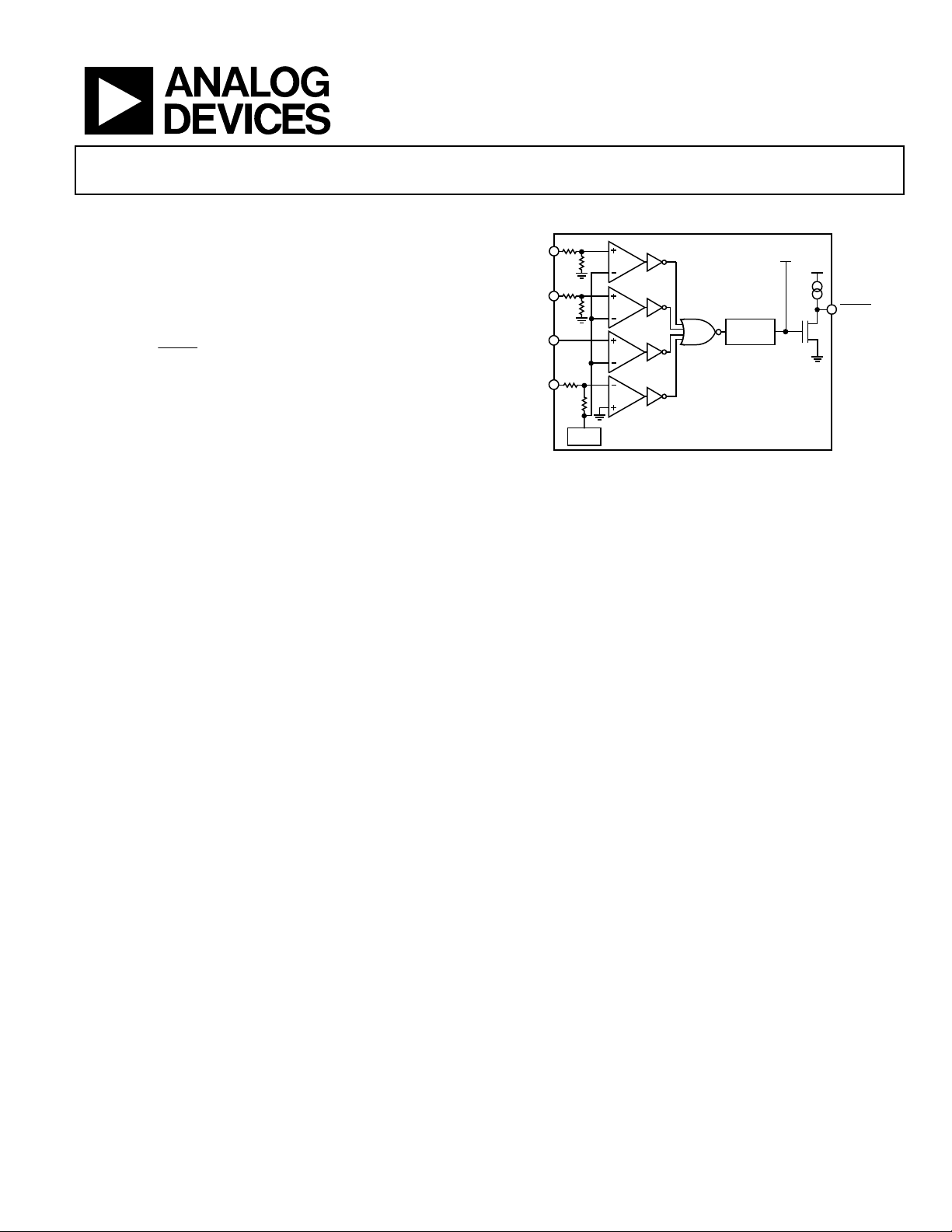
FUNCTIONAL BLOCK DIAGRAM
IN
IN
1
IN
2
200ms
IN
3
IN
4
V
REF
TIMEOUT
Figure 1.
1
5V PULLUP
ADM6339
IN
2
RESET
08169-001
GENERAL DESCRIPTION
The ADM6339 is a high accuracy supervisory circuit capable of
monitoring up to four system supply voltages.
The ADM6339 incorporates a variety of internally pretrimmed
undervoltage threshold options for monitoring −5.0 V, +1.8 V,
+2.5 V, +3.0 V, +3.3 V, and +5.0 V supply voltages. Tolerance levels
of ±5% and ±10% are available. The device is also available
with one to three adjustable threshold options. The adjustable
voltage threshold options are +1.23 V, +0.62 V, and −0.5 V. See
the Ordering Guide section for a list and description of all
available options.
If a monitored power supply voltage decreases below the minimum voltage threshold (or rises above the maximum voltage
threshold for the −0.5 V and −5.0 V input options), a single
active low output asserts, triggering a system reset. The output
is open drain with a weak internal pull-up to the monitored IN
supply of typically 10 µA. After all voltages exceed the selected
threshold level, the reset signal remains low for the reset
timeout period (200 ms typical).
The ADM6339 output remains valid as long as IN
or IN2 exceeds
1
1 V. Unused monitored inputs should not be allowed to float or
to be grounded; instead, they should be connected to a supply
voltage greater than their specified threshold voltages.
The ADM6339 is available in a 6-lead SOT-23 package. The
device operates over the extended temperature range of −40°C
to +85°C.
2
Rev. A
Information furnished by Analog Devices is believed to be accurate and reliable. However, no
responsibility is assumed by Analog Devices for its use, nor for any infringements of patents or other
rights of third parties that may result from its use. Specifications subject to change without notice. No
license is granted by implication or otherwise under any patent or patent rights of Analog Devices.
Trademarks and registered trademarks are the property of their respective owners.
One Technology Way, P.O. Box 9106, Norwood, MA 02062-9106, U.S.A.
Tel: 781.329.4700 www.analog.com
Fax: 781.461.3113 ©2009–2010 Analog Devices, Inc. All rights reserved.

ADM6339
http://www.BDTIC.com/ADI
TABLE OF CONTENTS
Features .............................................................................................. 1
Applications ....................................................................................... 1
Functional Block Diagram .............................................................. 1
General Description ......................................................................... 1
Revision History ............................................................................... 2
Specifications ..................................................................................... 3
Absolute Maximum Ratings ............................................................ 4
ESD Caution .................................................................................. 4
Pin Configuration and Function Descriptions ............................. 5
REVISION HISTORY
10/10—Rev. 0 to Rev. A
Added Figure 19 .............................................................................. 10
6/09—Revision 0: Initial Version
Typical Performance Characteristics ..............................................6
Theory of Operation .........................................................................8
Input Configuration ......................................................................8
Monitoring Negative Voltages < −5.0 V .....................................8
User Adjustable Threshold Options ...........................................8
RESET
Output Configuration .....................................................9
Outline Dimensions ....................................................................... 10
Ordering Guide .......................................................................... 10
Rev. A | Page 2 of 12
ADM6339
http://www.BDTIC.com/ADI
SPECIFICATIONS
V
= 1.0 V to 5.5 V, TA = −40°C to +85°C, unless otherwise noted. Typical values are V
IN2
Table 1.
Parameter Min Typ Max Units Test Conditions/Comments
OPERATING VOLTAGE RANGE (V
INPUT CURRENT
INx Input Current
55 115 μA V
−0.1 +0.1 μA V
0.4 1.5 μA V
−15 −20 μA V
−0.1 +0.1 μA V
−1 −3 −5 μA V
THRESHOLD VOLTAGE
Fixed Threshold Voltage (VTH) 4.50 4.63 4.75 V 5.0 V (−5% tolerance) threshold.
V
Decreasing 4.25 4.38 4.50 V 5.0 V (−10% tolerance) threshold.
INx
3.00 3.08 3.15 V 3.3 V (−5% tolerance) threshold.
2.85 2.93 3.00 V 3.3 V (−10% tolerance) threshold.
2.70 2.78 2.85 V 3.0 V (−5% tolerance) threshold.
2.55 2.63 2.70 V 3.0 V (−10% tolerance) threshold.
2.13 2.19 2.25 V 2.5 V (−10% tolerance) threshold.
1.53 1.58 1.62 V 1.8 V (−10% tolerance) threshold.
V
Increasing −4.75 −4.63 −4.50 V −5.0 V (+5% tolerance) threshold.
INx
−4.50 −4.38 −4.25 V −5.0 V (+10% tolerance) threshold.
Adjustable Threshold Voltage (VTH)
V
Decreasing 1.20 1.23 1.26 V
INx
0.615 0.620 0.625 V
V
Increasing −0.497 −0.487 −0.477 V −0.5 V threshold.
INx
RESET THRESHOLD HYSTERESIS (V
0.47 % VTH IN4, ADM6339Q model.
RESET THRESHOLD TEMPERATURE
COEFFICIENT (TCV
)
TH
INX to RESET DELAY (tRD) 30 μs V
RESET TIMEOUT PERIOD (tRP) 140 200 280 ms
RESET
OUTPUT LOW (VOL)
0.4 V V
RESET
OUTPUT HIGH (VOH)
RESET
OUTPUT HIGH SOURCE
CURRENT (I
1
The device is powered by Input IN2.
2
RESET
The
)
OH
output is guaranteed to be in the correct state for IN1 or IN2 down to 1 V.
1, 2
)
IN2
1.0
5.5 V
25 40 μA V
) 0.3 % VTH
HYST
60 ppm/°C
0.4 V V
0.4 V V
0.4 V V
0.4 V V
V
0.8 × V
IN2
10 μA
INx
IN2
also the device power supply. The supply splits into 25 μA for
the resistor divider and 30 μA for other circuits.
INx
IN1
INx
INx
INx
INx
V
INx
IN2
IN2
IN2
IN1
IN1
V
IN2
V
IN2
= 3.0 V to 3.3 V, TA = 25°C.
IN2
= nominal input voltage for 1.8 V, 2.5 V, and 5.0 V supplies.
= nominal input voltage for 3.0 V and 3.3 V supplies. V
= 0 V to V
(input threshold voltage = 1.23 V).
IN2
is
IN2
= 1.5 V (ADM6339K and ADM6639L models only).
= −5.0 V (INx input threshold voltage = −5.0 V).
= 0.62 V (INx input threshold voltage = 0.62 V).
= −0.5 V (INx input threshold voltage = −0.5 V).
= VTH to (VTH − 50 mV) for all inputs except −0.5 V and −5.0 V;
= VTH to (VTH + 50 mV) for −5.0 V and −0.5 V inputs only.
= 5.0 V, I
= 2.5 V, I
= V
=1V, V
=0 V, V
≥ 2.55 V, I
≥ 2.55 V,
= 1 V, I
IN1
SINK
SINK
= 0 V, I
IN2
= 1 V, I
IN2
RESET
SOURCE
= 2 mA.
= 1.2 mA.
= 50 μA.
SINK
= 20 μA
SINK
= 20 μA
SINK
= 6 μA,
not asserted.
RESET
not asserted.
Rev. A | Page 3 of 12
ADM6339
http://www.BDTIC.com/ADI
ABSOLUTE MAXIMUM RATINGS
Table 2.
Parameter Rating
VCC, RESET, GND
Continuous RESET Current
INx (Positive Reset Threshold) −0.3 V to +6 V
IN4 (Negative Reset Threshold, −5 V)
IN4 ADM6339Q Model (Negative Reset
Threshold,
Storage Temperature Range −65°C to +125°C
Operating Temperature Range −40°C to +85°C
Lead Temperature (10 sec) 300°C
Junction Temperature 135°C
Stresses above those listed under Absolute Maximum Ratings
may cause permanent damage to the device. This is a stress
rating only; functional operation of the device at these or any
other conditions above those indicated in the operational
section of this specification is not implied. Exposure to
absolute maximum rating conditions for extended periods may
affect device reliability.
−0.5 V)
−0.3 V to +6 V
20 mA
−6 V to +0.3 V
−2 V to +0.3 V
Table 3. Thermal Resistance
Package Type θJA Unit
6-Lead SOT-23 169.5 °C/W
ESD CAUTION
Rev. A | Page 4 of 12

ADM6339
http://www.BDTIC.com/ADI
PIN CONFIGURATION AND FUNCTION DESCRIPTIONS
IN
1
IN
2
IN
3
1
ADM6339
2
TOP VIEW
(Not to S cale)
3
6
5
4
RESET
GND
IN
4
08169-002
Figure 2. Pin Configuration
Table 4. Pin Function Descriptions
Pin No. Mnemonic Description
1 IN1 Monitored Input Voltage 1.
2 IN2 Monitored Input Voltage 2. IN2 is the power supply input for the ADM6339.
3 IN3 Monitored Input Voltage 3.
4 IN4 Monitored Input Voltage 4.
5 GND Ground.
6
Active Low RESET Output. RESET goes low when an input drops below the specified threshold (or above in the
RESET
case of the −0.5 V and −5.0 V input options). After all inputs rise above the threshold voltage, RESET
for 200 ms (typical) before going high. RESET
is open drain with a weak internal pull-up to IN2, typically 10 μA.
remains low
Rev. A | Page 5 of 12

ADM6339
http://www.BDTIC.com/ADI
TYPICAL PERFORMANCE CHARACTERISTICS
V
= VCC = 3.0 V, TA = 25°C, unless otherwise noted.
IN2
60
58
56
54
52
50
48
INPUT CURRENT (µ A)
2
46
IN
44
V
42
40
–40 85
–15 10 35 60
TEMPERATURE (ºC)
IN2
V
IN2
Figure 3. IN2 Input Current vs. Temperature
= 3.3V
= 3V
08169-010
100
90
80
70
60
50
40
TRANSIENT DURATION (µs)
X
30
20
10
MAXIMUM IN
0
01
100 200 300 400 500 600 700 800 900
RESET THRESHOLD OVERDRI V E ( mV )
RESET ASSERT ED ABOV E T HI S LINE
08169-012
000
Figure 6. Maximum INx Transient Duration vs. Reset Threshold Overdrive
120
100
80
60
40
INPUT CURRENT (µ A)
2
IN
20
0
05
0.5 1.0 1.5 2.0 2.5 3.0 3.5 4.0 4.5 5.0
IN2 VOLTAGE (V)
08169-011
.5
Figure 4. IN2 Input Current vs. IN2 Voltage
0.05
0
–0.05
–0.10
–0.15
NORMALIZED THRESHOLD E RRO R ( %)
–0.20
–40 –20 0 20 40 60 80
TEMPERATURE (°C)
5V
1.8V
08169-007
Figure 5. Normalized Threshold Error vs. Temperature
100
90
80
70
60
50
40
RESET DELAY (µs)
30
20
10
0
01
100 200 300 400 500 600 700 800 900
RESET
Figure 7.
214
212
210
208
206
RESET TIMEOUT DELAY (mS)
204
202
Delay vs. Reset Threshold Overdrive (INx Decreasing)
–40 85
Figure 8. Reset Timeout Delay vs. Temperature
RESET THRESHOLD OVERDRI V E ( mV )
–15103560
TEMPERATURE ( ºC)
08169-013
000
08169-014
Rev. A | Page 6 of 12

ADM6339
V
–
V
http://www.BDTIC.com/ADI
IN
C3
x
RESET
IN
C3
x
C2
C2 DC1M
BwL C3 DC1M
2.00V/div
–6.000V offset
RESET
Figure 9.
0.630
0.625
0.620
TRIP THRESHOL D ( V )
IN
0.615
0.62V
0.610
–40 –20 0 20 40 60 80
BwL Timebase 0.0µs
1.00V/div
2.040V offset
10.0 µs/div
2.0 GS/s200kS
Pull-Up and Pull-Down Response (10 μs/Div)
TEMPERATURE (°C)
Figure 10. 0.62 V Input Voltage Trip Threshold vs. Temperature
Trigger 0.0µs
–520mVSTOP
NEGATIVEEDGE
C2
08169-015
–0.495
–0.500
TRIP THRESHOL D ( V )
IN
–0.505
–0.5V
–0.510
8169-009
RESET
C2 DC1M
BwL C3
2.00V/div
–6.000V offset
Figure 11.
0.490
–40–200 20406080
BwL
DC1M –101ms C3Timebase
2.00V/div
2.000V offset
RESET
Timeout Delay (50 ms/Div)
TEMPERATURE (°C)
50.0 ms/div
1.0 MS/s500kS
Trigger DC
680mVNormal
PositiveEdge
08169-016
8169-008
Figure 12. −0.5 V Input Voltage Trip Threshold vs. Temperature
Rev. A | Page 7 of 12

ADM6339
V
http://www.BDTIC.com/ADI
THEORY OF OPERATION
The ADM6339 is a compact, low power supervisory circuit that
is capable of monitoring up to four voltages in a multisupply
application.
The device includes several factory-set voltage threshold options
f or m o n i t o r i n g − 5 . 0 V, +1 .8 V, + 2. 5 V, +3 . 0 V, + 3 . 3 V, a nd +5 .0 V
supplies. The ADM6339 is available with one to three adjustable
threshold options. The adjustable voltage threshold options
available are +1.23 V, +0.62 V, and −0.5 V. See the Ordering Guide
section for a list and description of all available options.
INPUT CONFIGURATION
Built-in hysteresis improves the ADM6339’s immunity to short
input transients, without noticeably reducing the threshold
accuracy. The internal comparators each have a hysteresis of
0.3% with respect to the reset threshold voltage. (The IN
input
4
of the ADM6339Q model has a hysteresis of 0.47% with respect
to its reset threshold voltage of −0.487 V.)
Monitored inputs are resistant to short power supply glitches.
Figure 6 depicts the ADM6339 glitch immunity data. To
increase noise immunity in noisy applications, place a 0.1 F
capacitor between the IN
to IN
, IN3, and IN4 also improves noise immunity.
1
MONITORED
SUPPLIES
Figure 13. Typical Applications Circuit
input and ground. Adding capacitance
2
ADM6339
IN
1
IN
2
RESET
IN
3
IN
4
GND
MICROPROCESSOR
08169-003
IN2 must always be used for normal operation because it is the
device’s power supply input. Do not allow unused monitor
inputs to float or to be grounded. Unused IN
positive thresholds can be connected directly to the IN
Unused IN
options with negative thresholds must be tied to a
4
or IN4 inputs with
3
input.
2
more negative supply.
MONITORING NEGATIVE VOLTAGES < −5.0 V
A number of ADM6339 models include a pretrimmed threshold
option to monitor −5.0 V voltage levels. Use a low impedance
resistor divider network similar to that shown in Figure 14 to
monitor supplies more negative than −5.0 V.
The current through the external resistor divider should be
greater than the input current for the −5.0 V monitor options.
For an input monitor current error of <1%, the resistor network
current should be greater than or equal to 2 mA (for I
maximum). Set R
V
reset threshold voltage, using the following equation:
INTH
= R2((V
R
1
= 2.5 k. Calculate R1 based on the desired
2
) − 1)
INTH/VTH
= 20 µA
IN4
where:
R
≤ 2.49 k.
2
V
is the desired threshold voltage.
INTH
V
is the internal threshold voltage.
TH
For example, when monitoring a nominal voltage of −12 V,
V
= −11.1 V, VTH = −4.63 V, and R2 = 2.49 k. Therefore,
INTH
using the previous equation, R
R
2
R
1
V
INTH
Figure 14. Negative Voltage Monitoring
= 3.48 k.
1
ADM6339
08169-004
USER ADJUSTABLE THRESHOLD OPTIONS
The ADM6339 offers the choice of three adjustable INx input
threshold voltages: +1.23 V, +0.62 V, or −0.5 V.
When using an adjustable threshold of 1.23 V (typical), to
monitor a voltage greater than 1.23 V, connect a resistor divider
network to the device as shown in Figure 15. V
threshold voltage, can be expressed as
V
= 1.23 V((R1 + R2)/(R2))
INTH
The ADM6339 has a guaranteed input current of ±0.1 µA on its
1.23 V adjustable input. Resistor values up to 100 k can be
used for R
with <1% error.
2
INTH
1
2
ADM6339
V
= 1.23V
REF
R
R
Figure 15. Setting the 1.23 V Adjustable Monitor
The same approach is taken when using the 0.62 V (typical)
adjustable threshold input. Use the following equation to solve
for the values of R
V
= 0.62 V((R1 + R2)/(R2))
INTH
and R2:
1
The 0.62 V (typical) adjustable threshold input offers high
threshold accuracy of ±0.8%.
INTH
8169-005
, the desired
Rev. A | Page 8 of 12

ADM6339
V
V
http://www.BDTIC.com/ADI
When monitoring a voltage more negative than −0.5 V, a
scheme similar to that previously described in the Monitoring
Negative Voltages < −5.0 V section is used. For an input
monitor current error of <1%, the resistor network current
should be ≥500 µA (for I
based on the desired V
= 5 µA maximum). Calculate R1
IN4
reset threshold voltage, using the
INTH
following equation:
R
where V
= R2((V
1
INTH/VTH
is the desired threshold voltage and VTH is the
INTH
) − 1)
internal threshold voltage, −0.487 V (typical).
RESET OUTPUT CONFIGURATION
RESET
The
drops below its voltage threshold (or goes above its associated
threshold in the case of the −0.5 V and −5.0 V input options).
After all voltages exceed their associated threshold level, the
reset signal remains low for the reset timeout period, t
(200 ms typical).
output asserts low if a monitored INx voltage
IN
V
x
TH
RP
RESET
is open drain with a weak internal pull-up to IN2 of
10 A (typical). Many applications that interface with other
logic devices do not require an external pull-up resistor.
However, if an external pull-up resistor is required and it is
connected to a voltage ranging from 0 V to 5.5 V, the resistor
overdrives the internal pull-up. Reverse current flow from the
external pull-up voltage to IN
is prevented by the internal
2
circuitry.
V
RESET
5
CC
08169-006
IN2= 3.3
ADM6339
Figure 17. Interfacing with a Different Logic Supply Voltage
100kΩ
RESET
RESET
t
RD
10%
Figure 16. ADM6339
RESET
t
RP
Timing
90%
08169-017
Rev. A | Page 9 of 12

ADM6339
0
0
http://www.BDTIC.com/ADI
OUTLINE DIMENSIONS
INDICATOR
.15 MAX
.05 MIN
1.30
1.15
0.90
3.00
2.90
2.80
1.70
1.60
1.50
PIN 1
65
123
4
1.90
BSC
0.50 MAX
0.30 MIN
COMPLIANT TO JEDEC STANDARDS MO-178-AB
0.95 BSC
1.45 MAX
0.95 MIN
3.00
2.80
2.60
SEATING
PLANE
0.20 MAX
0.08 MIN
Figure 18. 6-Lead Small Outline Transistor Package [SOT-23]
(RJ-6)
Dimensions shown in millimeters
ROUND SPROCKET HOLES
PIN 1 MARKER
10°
0.55
0.60
4°
BSC
0°
0.45
0.35
121608-A
DIRECTION OF FEED
08169-018
Figure 19. ADM6339 Reel Orientation
ORDERING GUIDE
1, 2
Model
ADM6339AARJZ-RL7 5.0 3.3 2.5 Adj (1.23) 10 −40°C to +85°C 6-Lead SOT-23 RJ-6 MBF
ADM6339BARJZ-RL7 5.0 3.3 2.5 Adj (1.23) 5 −40°C to +85°C 6-Lead SOT-23 RJ-6 MBH
ADM6339CARJZ-RL7 5.0 3.3 1.8 Adj (1.23) 10 −40°C to +85°C 6-Lead SOT-23 RJ-6 MBJ
ADM6339DARJZ-RL7 5.0 3.3 1.8 Adj (1.23) 5 −40°C to +85°C 6-Lead SOT-23 RJ-6 MBK
ADM6339EARJZ-RL7 5.0 3.0 2.5 Adj (1.23) 10 −40°C to +85°C 6-Lead SOT-23 RJ-6 MBL
ADM6339FARJZ-RL7 5.0 3.0 2.5 Adj (1.23) 5 −40°C to +85°C 6-Lead SOT-23 RJ-6 MBM
ADM6339GARJZ-RL7 5.0 3.0 1.8 Adj (1.23) 10 −40°C to +85°C 6-Lead SOT-23 RJ-6 MBN
ADM6339HARJZ-RL7 5.0 3.0 1.8 Adj (1.23) 5 −40°C to +85°C 6-Lead SOT-23 RJ-6 MBP
ADM6339IARJZ-RL7 5.0 3.3 2.5 1.8 10 −40°C to +85°C 6-Lead SOT-23 RJ-6 MBQ
ADM6339JARJZ-RL7 5.0 3.3 2.5 1.8 5 −40°C to +85°C 6-Lead SOT-23 RJ-6 MBR
ADM6339KARJZ-RL7 Adj (1.23) 3.3 2.5 Adj (1.23) 10 −40°C to +85°C 6-Lead SOT-23 RJ-6 MBS
ADM6339LARJZ-RL7 Adj (1.23) 3.3 2.5 Adj (1.23) 5 −40°C to +85°C 6-Lead SOT-23 RJ-6 MBU
ADM6339MARJZ-RL7 5.0 3.0 Adj (1.23) −5.0 10 −40°C to +85°C 6-Lead SOT-23 RJ-6 MB6
ADM6339NARJZ-RL7 5.0 3.0 Adj (1.23) −5.0 5 −40°C to +85°C 6-Lead SOT-23 RJ-6 MB7
ADM6339OARJZ-RL7 5.0 3.3 Adj (1.23) −5.0 10 −40°C to +85°C 6-Lead SOT-23 RJ-6 MB8
ADM6339PARJZ-RL7 5.0 3.3 Adj (1.23) −5.0 5 −40°C to +85°C 6-Lead SOT-23 RJ-6 MB5
ADM6339QARJZ-RL7 Adj (0.62) 3.3 Adj (0.62) Adj (−0.5) 10 −40°C to +85°C 6-Lead SOT-23 RJ-6 MBX
1
Z = RoHS Compliant Part.
2
Nominal input voltage is specified with 10% tolerance.
Nominal Input Voltage (V)
To le ra n ce
(%)
Temperature
Range
Package
Description
Package
Option
Branding IN1 IN2 IN3 IN4
Rev. A | Page 10 of 12

ADM6339
http://www.BDTIC.com/ADI
NOTES
Rev. A | Page 11 of 12

ADM6339
http://www.BDTIC.com/ADI
NOTES
©2009–2010 Analog Devices, Inc. All rights reserved. Trademarks and
registered trademarks are the property of their respective owners.
D08169-0-10/10(A)
Rev. A | Page 12 of 12
 Loading...