Supervisory Circuits with Watchdog
and Manual Reset in 5-Lead SOT-23
ADM6316/ADM6317/ADM6318/ADM6319/ADM6320/ADM6321/ADM6322
FEATURES
26 reset threshold options:
2.5 V to 5 V in 100 mV increments
4 reset timeout options:
1 ms, 20 ms, 140 ms, and 1120 ms (min)
V
CC
4 watchdog timeout options:
6.3 ms, 102 ms, 1600 ms, and 25.6s (typ)
Manual reset input
Reset output stages:
MR
Push-pull active-low
Open-drain active-low
Push-pull active-high
Low power consumption (5 µA)
Guaranteed reset output valid to V
Power supply glitch immunity
Specified over industrial temperature range
= 1 V
CC
5-lead SOT-23 package
APPLICATIONS
Microprocessor systems
Computers
Controllers
Intelligent instruments
Portable equipment
GENERAL DESCRIPTION
The ADM6316/ADM6317/ADM6318/ADM6319/ADM6320/
ADM6321/ADM6322 are supervisory circuits, which monitor
power supply voltage levels and code execution integrity in
microprocessor-based systems. As well as providing power on
reset signals, an on-chip watchdog timer can reset the microprocessor if it fails to strobe within a preset timeout period. A
reset signal can also be asserted by an external push-button,
through a manual reset input. The seven parts feature different
combinations of watchdog input, manual reset input, and
output stage configuration, as shown in Table 1.
Table 1. Selection Table
Part No. Watchdog Manual Reset
ADM6316 Yes Yes Push-Pull –
ADM6317 Yes Yes – Push-Pull
ADM6318 Yes – Push-Pull Push-Pull
ADM6319 – Yes Push-Pull Push-Pull
ADM6320 Yes Yes Open-Drain –
ADM6321 Yes - Open-Drain Push-Pull
ADM6322 – Yes Open-Drain Push-Pull
Each part is available in a choice of 26 reset threshold options
ranging from 2.5 V to 5 V in 100 mV increments. There are also
four reset timeout options of 1 ms, 20 ms, 140 ms, and 1120 ms
(min) and four watchdog timeout options of 6.3 ms, 102 ms,
1600 ms, and 25.6s (typ).
The ADM6316–ADM6322 are available in 5-lead SOT-23
packages and typically consume only 3 µA, making them
suitable for use in low power portable applications.
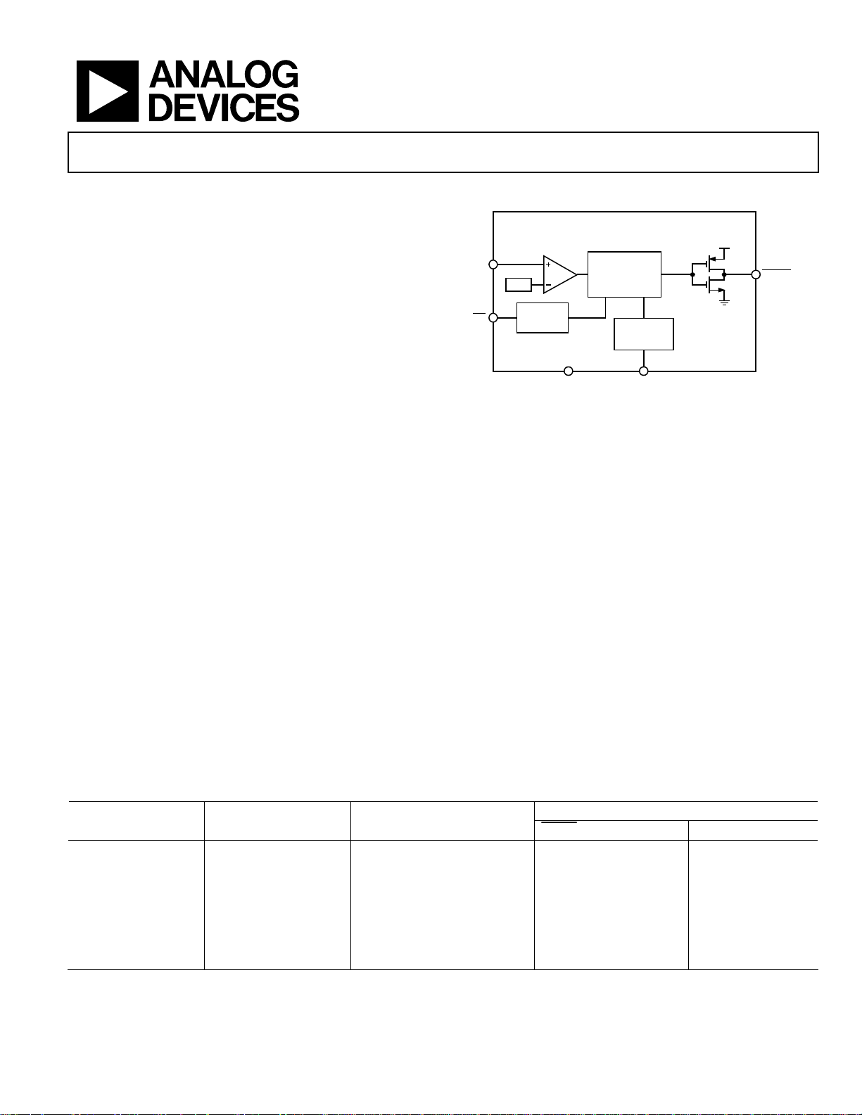
FUNCTIONAL BLOCK DIAGRAM
ADM6316
RESET
V
REF
DEBOUNCE
RESET
GENERATOR
WATCHDOG
DETECTOR
GND WDI
Figure 1.
Output Stage
V
CC
RESET
RESET
04533-0-001
Rev. 0
Information furnished by Analog Devices is believed to be accurate and reliable.
However, no responsibility is assumed by Analog Devices for its use, nor for any
infringements of patents or other rights of third parties that may result from its use.
Specifications subject to change without notice. No license is granted by implication
or otherwise under any patent or patent rights of Analog Devices. Trademarks and
registered trademarks are the property of their respective owners.
One Technology Way, P.O. Box 9106, Norwood, MA 02062-9106, U.S.A.
Tel: 781.329.4700
Fax: 781.326.8703 © 2004 Analog Devices, Inc. All rights reserved.
www.analog.com

ADM6316/ADM6317/ADM6318/ADM6319/ADM6320/ADM6321/ADM6322
TABLE OF CONTENTS
Specifications..................................................................................... 3
Watch d og I nput .......................................................................... 10
Absolute Maximum Ratings............................................................ 5
ESD Caution.................................................................................. 5
Pin Configurations and Function Descriptions ........................... 6
Typical Performance Characteristics ............................................. 7
Circuit Description......................................................................... 10
Reset Output ............................................................................... 10
Open-Drain
Manual Reset Input ....................................................................10
RESET
Output...................................................... 10
REVISION HISTORY
10/04—Revision 0: Initial Version
Application Information................................................................ 11
Watch d og I nput C ur r ent ........................................................... 11
Negative-Going V
Ensuring Reset Valid to V
Watchdog Software Considerations......................................... 11
Outline Dimensions ....................................................................... 12
Ordering Guide .......................................................................... 12
Transie n t s ................................................ 11
CC
= 0 V........................................... 11
CC
Rev. 0 | Page 2 of 12

ADM6316/ADM6317/ADM6318/ADM6319/ADM6320/ADM6321/ADM6322
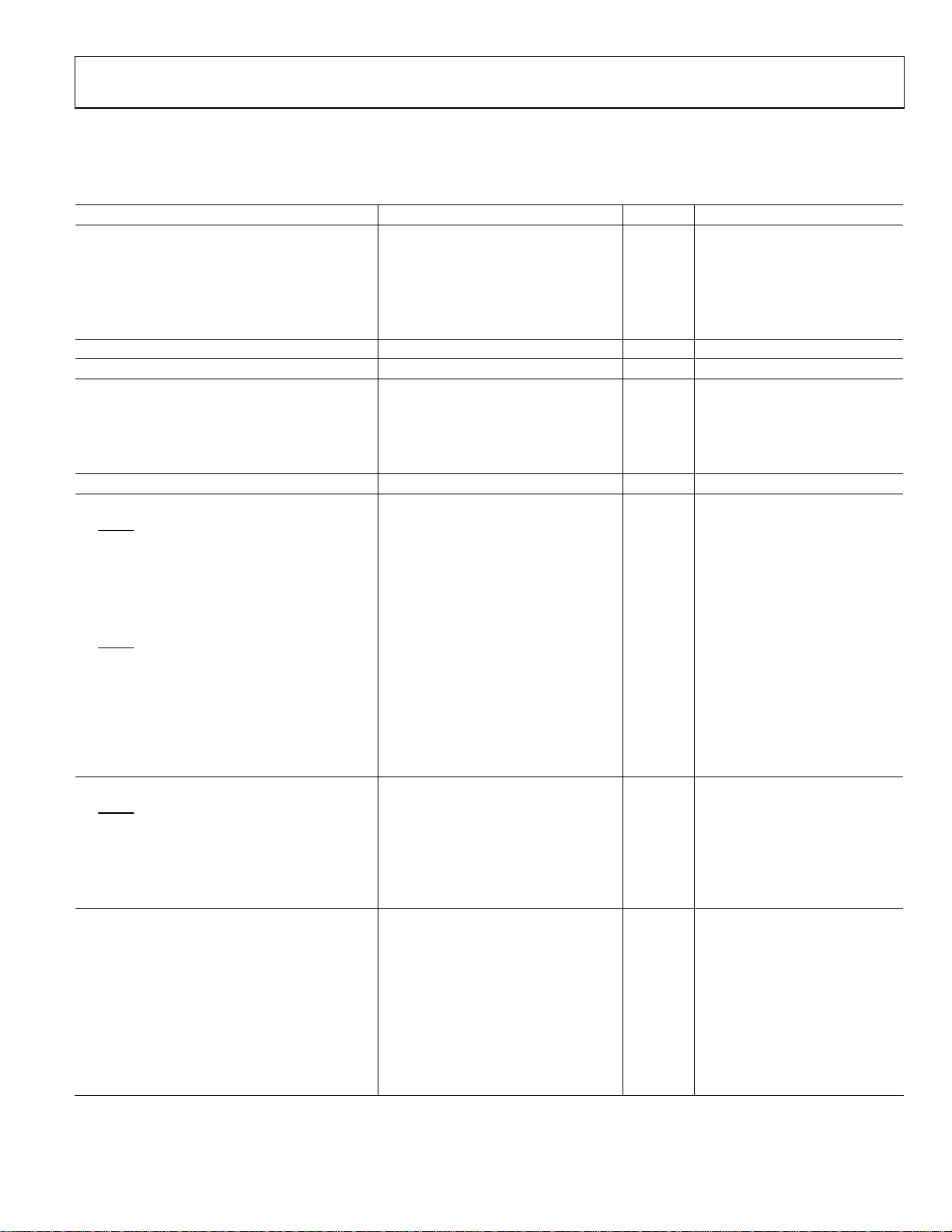
SPECIFICATIONS
VCC = full operating range, TA = T
Table 2.
Parameter Min Typ Max Unit Test Conditions/Comments
SUPPLY
VCC Operating Voltage Range 1 5.5 V
Supply Current 10 20 µA VCC = 5.5 V
5 12 µA VCC = 3.6 V
RESET THRESHOLD VOLTAGE
RESET THRESHOLD TEMPERATURE COEFFICIENT 40 ppm/°C
RESET THRESHOLD HYSTERESIS 3 mV
RESET TIMEOUT PERIOD
ADM63__A 1 1.4 2 ms
ADM63__B 20 28 40 ms
ADM63__C 140 200 280 ms
ADM63__D 1120 1600 2240 ms
VCC TO RESET DELAY 40 µs VCC falling at 1 mV/µs
PUSH-PULL OUTPUT (ADM6316, ADM6317,
ADM6318, ADM6319, ADM6321, ADM6322)
RESET Output Voltage
0.3 V
0.3 V VCC ≥ 2.7 V, I
0.4 V VCC ≥ 4.5 V, I
0.8 × V
V
RESET Rise Time
RESET Output Voltage 0.3 V VCC ≥ 2.7 V, I
0.4 V VCC ≥ 4.5 V, I
0.8 × V
0.8 × V
V
OPEN-DRAIN OUTPUT (ADM6320, ADM6321,
ADM6322)
RESET Output Voltage
0.3 V VCC ≥ 1.2 V, I
0.3 V VCC ≥ 2.7 V, I
0.4 V VCC ≥ 4.5 V, I
Open-Drain Reset Output Leakage Current 1 µA
WATCHDOG INPUT (ADM6316, ADM6317,
ADM6318, ADM6320, ADM6321)
Watchdog Timeout Period 4.3 6.3 9.3 ms ADM63___W
71 102 153 ms ADM63___X
1.12 1.6 2.4 s ADM63___Y
17.9 25.6 38.4 s ADM63___Z
WDI Pulse Width 50 ns VIL = 0.3 × VCC, VIH = 0.7 × V
WDI Input Threshold 0.3 × V
WDI Input Current 120 160 µA V
to T
MIN
, unless otherwise noted.
MAX
VTH − 1.5% V
VTH − 2.5% V
TH
TH
VTH + 1.5% V TA = +25°C
VTH + 2.5% V TA = −40°C to +85°C
0.3 V
V V
CC
− 1.5 V VCC ≥ 4.5 V, I
CC
5 25 ns
V V
CC
V V
CC
– 1.5 V VCC ≥ 4.5 V, I
CC
V
≥ 1.0 V, I
CC
V
≥ 1.2 V, I
CC
≥ 2.7 V, I
CC
= 50 µA
SINK
= 100 µA
SINK
= 1.2 mA
SINK
= 3.2 mA
SINK
SOURCE
SOURCE
= 500 µA
= 800 µA
From 10% to 90% VCC, CL = 5 pF,
V
= 3.3 V
CC
= 1.2 mA
SINK
= 3.2 mA
SINK
≥ 1.8 V, I
CC
≥ 2.7 V, I
CC
SOURCE
SOURCE
SOURCE
= 150 µA
= 500 µA
= 800 µA
0.3 V V
0.7 × V
CC
V
CC
−20 −15 µA V
≥ 1.0 V, I
CC
= VCC, time average
WDI
= 0, time average
WDI
= 50 µA
SINK
= 100 µA
SINK
= 1.2 mA
SINK
= 3.2 mA
SINK
CC
Rev. 0 | Page 3 of 12

ADM6316/ADM6317/ADM6318/ADM6319/ADM6320/ADM6321/ADM6322
Parameter Min Typ Max Unit Test Conditions/Comments
MANUAL RESET INPUT (ADM6316, ADM6317,
ADM6319, ADM6320, ADM6322)
MR Input Threshold
0.3 × V
MR Input Pulse Width
MR Glitch Rejection
MR Pull-up Resistance
MR to Reset Delay
0.8 2.0 V V
0.7 × V
CC
V VTH < 4.0 V
CC
> 4.0 V
TH
1 µs
100 ns
35 52 75 kΩ
230 ns V
= 5 V
CC
Rev. 0 | Page 4 of 12
 Loading...