

Page 1
Open-Drain Microprocessor
V
www.BDTIC.com/ADI
FEATURES
Specified over temperature
Low power consumption (5 μA typical)
Precision voltage monitor of voltages from 2.5 V to 5 V
a
t 100 mV increments
Reset assertion down to V
Reset timeout periods: 1 ms, 20 ms, 140 ms,
or 1120 ms
(minimum)
Built-in manual reset
Pin compatible with the ADM811
Available in SOT-143 package
APPLICATIONS
Microprocessor systems
Controllers
Intelligent instruments
Automotive systems
Safety systems
Portable instruments
> 1 V
CC
Supervisory Circuit in 4-Lead SOT-143
ADM6315
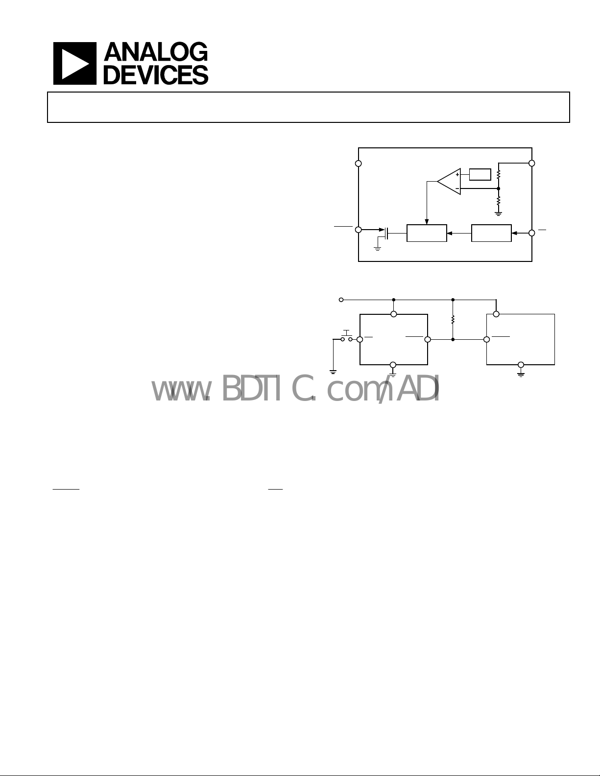
FUNCTIONAL BLOCK DIAGRAM
SYSTEM
V
CC
MR
00081-001
CC
GND
RESET
V
ADM6315
RESET
CIRCUITRY
Figure 1.
ADM6315
MR
RESET
GND GND
Figure 2. Typical Operating Circuit
10kΩ
REF
DEBOUNCE
SYSTEM POWER
MICROPROCESSOR
RESET
00081-011
GENERAL DESCRIPTION
The ADM6315 is a reliable voltage-monitoring device that is
suitable for use in most voltage-monitoring applications.
The ADM6315 is designed to monitor as little as a 1.8%
deg
radation of a power supply voltage. The ADM6315 can
monitor all voltages (at 100 mV increments) from 2.5 V to 5 V.
Included in this circuit is a debounced manual reset input.
RESET
can be activated using an ordinary switch (pulling MR
low), a low input from another digital device, or a degradation
of the supply voltage.
The manual reset function is very useful, especially if the circuit
in
which the ADM6315 is operating enters into a state that can
be detected only by the user. Allowing the user to reset a system
manually can reduce the damage or danger that could otherwise
be caused by an out-of-control or locked-up system.
The ADM6315 is available in a cost- and space-efficient
T-143 package.
SO
Rev. E
Information furnished by Analog Devices is believed to be accurate and reliable. However, no
responsibility is assumed by Anal og Devices for its use, nor for any infringements of patents or ot her
rights of third parties that may result from its use. Specifications subject to change without notice. No
license is granted by implication or otherwise under any patent or patent rights of Analog Devices.
Trademarks and registered trademarks are the property of their respective owners.
One Technology Way, P.O. Box 9106, Norwood, MA 02062-9106, U.S.A.
Tel: 781.329.4700 www.analog.com
Fax: 781.461.3113 ©1999–2007 Analog Devices, Inc. All rights reserved.
Page 2

ADM6315
www.BDTIC.com/ADI
TABLE OF CONTENTS
Features.............................................................................................. 1
Applications....................................................................................... 1
Functional Block Diagram .............................................................. 1
General Description ......................................................................... 1
Revision History ............................................................................... 2
Specifications..................................................................................... 3
Absolute Maximum Ratings............................................................ 4
Thermal Resistance ...................................................................... 4
ESD Caution.................................................................................. 4
Pin Configuration and Function Descriptions............................. 5
REVISION HISTORY
9/07—Rev. D to Rev. E
Changes to Absolute Maximum Ratings....................................... 4
Updated Outline Dimensions......................................................... 8
Changes to Ordering Guide............................................................ 8
4/06—Rev. C to Rev. D
pdated Format..................................................................Universal
U
Updated Outline Dimensions......................................................... 8
Changes to Ordering Guide............................................................ 8
12/03—Rev. B to Rev. C
E
dit to Absolute Maximum Ratings............................................... 3
Edits to Ordering Guide .................................................................. 4
Deleted Table I and Table II ............................................................ 6
Deleted Table III and Table IV........................................................ 7
Updated Outline Dimensions......................................................... 8
Typical Performance Characteristics..............................................6
Theory of Operation .........................................................................7
Interfacing to Output of Other Devices .....................................7
Benefits of a Very Accurate
Detailed Description.....................................................................7
Manual Reset Input.......................................................................7
Transient Immunity ......................................................................7
Outline Dimensions..........................................................................8
Ordering Guide .............................................................................8
2/03—Rev. A to Rev. B
E
dits to Features.................................................................................1
Edits to Specifications.......................................................................2
Edits to Absolute Maximum Ratings..............................................3
Edits to Ordering Guide...................................................................3
Edits to Table I and Table II .............................................................6
Edits to Table III and Table IV.........................................................7
Updated Outline Dimensions..........................................................8
10/01—Rev. 0 to Rev. A
dits to Table III ................................................................................7
E
Edits to Table IV ................................................................................7
1999—Revision 0: Initial Version
RESET
Threshold .............................7
Rev. E | Page 2 of 12
Page 3
ADM6315
www.BDTIC.com/ADI
SPECIFICATIONS
VCC = full operating range, TA = T
Table 1.
Parameter Min Typ Max Unit Test Conditions/Comments
SUPPLY
Operating Voltage 1 5.5 V TA = −40°C to +85°C
VCC Supply Current 5 12 μA VCC = 5.5 V, no load, TA = −40°C to +85°C
15 μA VCC = 5.5 V, no load, TA = −40°C to +125°C
4 10 μA VCC = 3.6 V, no load, TA = −40°C to +85°C
12 μA VCC = 3.6 V, no load, TA = −40°C to +125°C
RESET VOLTAGE THRESHOLD (VTH)
V
V
RESET THRESHOLD TEMPERATURE COEFFICIENT
VCC TO RESET DELAY 35 μs VCC = falling at 1 mV/μs
RESET ACTIVE TIMEOUT PERIOD
ADM6315xxD1 1 1.4 2 ms TA = −40°C to +85°C
0.8 2.4 ms TA = −40°C to +125°C
ADM6315xxD2 20 28 40 ms TA = −40°C to +85°C
16 48 ms TA = −40°C to +125°C
ADM6315xxD3 140 200 280 ms TA = −40°C to +85°C
112 336 ms TA = −40°C to +125°C
ADM6315xxD4 1120 1570 2240 ms TA = −40°C to +85°C
896 2688 ms TA = −40°C to +125°C
MANUAL RESET
Input Threshold 0.8 V VTH > 4 V (VIL)
2.4 V VTH > 4 V (VIH)
0.3 × VCC V VTH < 4 V (VIL)
0.7 × VCC V VTH < 4 V (VIH)
Minimum Input Pulse 1 μs
Glitch Rejection 100 ns
To Reset Delay 500 ns
Pull-Up Resistance 32 63 100 kΩ
RESET OUTPUT
Output Voltage 0.4 V VCC > 4.25 V, I
0.3 V VCC > 2.5 V, I
0.3 V VCC > 1 V, I
Output Leakage Current 1 μA
MIN
to T
, VCC typical = 5 V, unless otherwise noted.
MAX
V
− 1.8% VTH VTH + 1.8% V TA = 25°C
TH
− 2.5% VTH + 2.5% V TA = −40°C to +85°C
TH
− 3.5% VTH + 3.5% V TA = −40°C to +125°C
TH
60 ppm/°C
= 3.2 mA
SINK
= 1.2 mA
SINK
= 80 μA
SINK
> VTH, RESET deasserted
V
CC
Rev. E | Page 3 of 12
Page 4
ADM6315
www.BDTIC.com/ADI
ABSOLUTE MAXIMUM RATINGS
TA = 25°C, unless otherwise noted.
Table 2.
Parameter Rating
Terminal Voltage (with Respect to Ground)
VCC −0.3 V to +6 V
All Other Inputs −0.3 V to +6 V
Input Current
20 mA
V
CC
Output Current
RESET
Operating Temperature Range −40°C to +125°C
Storage Temperature Range −65°C to +160°C
Lead Temperature (Soldering, 10 sec) 300°C
Vapor Phase (60 sec) 215°C
Infrared (15 sec) 220°C
ESD Rating 2.5 kV
Stresses above those listed under Absolute Maximum Ratings
y cause permanent damage to the device. This is a stress
ma
rating only; functional operation of the device at these or any
other conditions above those indicated in the operational
section of this specification is not implied. Exposure to absolute
maximum rating conditions for extended periods may affect
device reliability.
20 mA
THERMAL RESISTANCE
θJA is specified for the worst-case conditions, that is, a device
soldered in a circuit board for surface-mount packages.
Table 3. Thermal Resistance
Package Type θ
4-Lead SOT-143 330 °C/W
Unit
JA
ESD CAUTION
Rev. E | Page 4 of 12
Page 5

ADM6315
www.BDTIC.com/ADI
PIN CONFIGURATION AND FUNCTION DESCRIPTIONS
1
GND
2
RESET
Figure 3. Pin Configuration
Table 4. Pin Function Descriptions
Pin No. Mnemonic Description
1 GND Ground Reference for All Signals, 0 V.
2
Active Low Logic Output. RESET remains low while VCC is below the reset threshold or when MR is low. RESET
RESET
then remains low for a minimum of 1 ms, 20 ms, 140 ms, or 1120 ms after VCC rises above the reset threshold
and MR
is high.
3
Manual Reset. This active low debounced input ignores input pulses of 100 ns (typical) and is guaranteed to
MR
accept input pulses of greater than 1 μs. Leave floating when not used.
4 V
Monitored Supply Voltage.
CC
ADM6315
TOP VIEW
(Not to Scale)
V
4
CC
3
MR
00081-002
Rev. E | Page 5 of 12
Page 6

ADM6315
www.BDTIC.com/ADI
TYPICAL PERFORMANCE CHARACTERISTICS
10
8
= 5.5V
V
CC
6
(µA)
DD
I
4
2
0
–20 0 20 40 60 80 100 125
–40
= 3V
V
CC
V
= 1V
CC
TEMPERATURE (° C)
Figure 4. Supply Current vs. Temperature
00081-003
50
45
40
35
30
25
20
15
10
MAXIMUM TRANSI ENT DURATI ON (µs)
5
0
0 100 200 300 400 500 600 700 800 900 1000
RESET COMPARATOR OVERDRIVE, (VTH– VCC) (mV)
RESET
Figure 7. Maximum Transient Durati on vs.
Comparator Overdrive
00081-012
450
400
350
300
250
200
150
100
POWER-DOWN RESET DELAY (µs)
50
0
–40
–20 0 20 40 60 80 100 125
1.06
1.04
1.02
1.00
0.98
0.96
NORMALIZED RESET TIMEOUT PERIOD (ms)
0.94
–40
–20 0 20 40 60 80 100 125
TEMPERATURE (° C)
TEMPERATURE (° C)
V
OD
V
OD
VOD = 20mV
= 125mV
= 200mV
Figure 6. Normalized Reset Timeout Period vs. Temperature (V
Rising)
CC
1.005
1.000
0.995
NORMALIZED RESET THRESHO LD (V)
0.990
–40 –20 0 20 40 60 80 100 125
00081-004
Figure 8. Normalized Reset Threshold vs. Temperature (V
12
10
8
6
4
SUPPLY CURRENT (µA)
2
0
0
0081-005
TEMPERATURE ( °C)
1
SUPPLY VOLTAGE (V)
00081-007
Falling) Figure 5. Power-Down Reset Delay vs. Temperature
CC
+85°C
4
–40°C
5
0081-008
+25°C
2
3
Figure 9. Supply Current vs. Supply Voltage
Rev. E | Page 6 of 12
Page 7

ADM6315
V
www.BDTIC.com/ADI
THEORY OF OPERATION
INTERFACING TO OUTPUT OF OTHER DEVICES
The ADM6315 series is designed to integrate with as many devices
RESET
as p
ossible. One feature of the ADM6315 is the
opendrain output, which can sink current from sources with a
voltage greater than the V
of the ADM6315 input, making it
CC
suitable for use in more diverse applications.
BENEFITS OF A VERY ACCURATE RESET THRESHOLD
Because the ADM6315 series can operate effectively even when
there are large degradations of the supply voltages (due to an
accurate internal voltage reference circuit), the possibility of a
malfunction during a power failure is greatly reduced.
CC
TRIP POINT (MAX)
V
CC
RESET
Figure 10. V
TRIP POINT
V
CC
V
TO RESET
CC
DELAY
Power-Down/Brownout Timing Diagram
CC
VCC TRIP POINT (MIN)
VOL
00081-009
DETAILED DESCRIPTION
The ADM6315 is designed to protect the integrity of a system’s
operation by ensuring the proper operation of the system
during power-up, power-down, and brownout conditions.
When the ADM6315 is powered up, the
ADM6315 remains low for a period typically equal to the
active timeout period. This feature allows adequate time for the
system to power up correctly and for the power supply to
stabilize before any devices are brought out of reset and allowed
to begin executing instructions. Initializing a system in this way
provides a more reliable startup for microprocessor systems.
When a brownout condition occurs (assuming V
1 mV/μs), the ADM6315 produces a reset in 35 μs typical.
Producing a reset this fast means that the entire system can be
reset together before any part of the system’s voltage falls below
its recommended operating voltage. This system reset can avoid
dangerous and/or erroneous operation of a microprocessorbased system.
RESET
output of the
RESET
is falling at
CC
MANUAL RESET INPUT
The ADM6315 also provides an additional input, MR. This
input can be used either as a means for the system operator to
reset the system manually via a switch or for a digital circuit to
reset the system.
MR
The
input (typically) ignores negative-going pulses that are
faster than 100 ns, and it is guaranteed to accept any negativegoing input pulse of a duration greater than or equal to 1 μs. If
MR
is connected to long cables or is used in a noisy environment,
placing a 1 μF decoupling capacitor between the
MR
input and
ground further improves the glitch immunity of the ADM6315.
VCC TRIP POINT (MAX)
TRIP POINT
V
VCC TRIP POINT (MIN)
V
CC
RESET
Figure 11. V
CC
RESET ACTIVE TIMEOUT
Power-Up Timing Diagram
CC
00081-010
TRANSIENT IMMUNITY
As well as being an accurate reset circuit, the ADM6315 has
go
od immunity from negative-going transients (see Figure 7).
ecause of this characteristic, the ADM6315 is suitable for use
B
in noisy environments.
Figure 7 shows the
magnitude of negative-going pulses with respect to the typical
reset threshold) vs. the pulse duration without a reset.
RESET
comparator overdrive (the maximum
Rev. E | Page 7 of 12
Page 8

ADM6315
www.BDTIC.com/ADI
OUTLINE DIMENSIONS
3.04
2.90
2.80
0.20
BSC
1.40
1.30
1.20
1.22
0.80
4
12
1.92 BSC
0.89
0.76
COMPLIANT TO JEDEC STANDARDS TO-253-AA
2.64
3
2.10
1.07
0.90
0.75
0.50
0.30
0.100
0.013
SEATING
PLANE
0.20
0.08
0.54 REF
0.60
0.50
0.40
8°
0°
073105-A
Figure 12. 4-Lead Small Outline Transistor Package [SOT-143]
(RA-4)
Dim
ensions shown in millimeters
ORDERING GUIDE
Temperature
Range
ription Branding
ADM6315-46D1ARTRL7 −40°C to +125°C 4-Lead Small Outline Transistor [SOT-143] RA-4 4.63 1 MDV
ADM6315-46D1ART-RL −40°C to +125°C 4-Lead Small Outline Transistor [SOT-143] RA-4 4.63 1 MDV
ADM6315-46D1ARTZR7
−40°C to +125°C 4-Lead Small Outline Transistor [S
OT-143] RA-4 4.63 1 M9Q
1
ADM6315-45D1ARTRL7 −40°C to +125°C 4-Lead Small Outline Transistor [SOT-143] RA-4 4.50 1 MDU
ADM6315-45D1ART-RL −40°C to +125°C 4-Lead Small Outline Transistor [SOT-143] RA-4 4.50 1 MDU
ADM6315-45D1ARTZR7 −40°C to +125°C 4-Lead Small Outline Transistor [S
1
OT-143] RA-4 4.50 1 M81
ADM6315-44D1ARTRL7 −40°C to +125°C 4-Lead Small Outline Transistor [SOT-143] RA-4 4.39 1 MDT
ADM6315-44D1ART-RL −40°C to +125°C 4-Lead Small Outline Transistor [SOT-143] RA-4 4.39 1 MDT
ADM6315-31D1ARTRL7 −40°C to +125°C 4-Lead Small Outline Transistor [SOT-143] RA-4 3.08 1 MDG
ADM6315-31D1ART-RL −40°C to +125°C 4-Lead Small Outline Transistor [SOT-143] RA-4 3.08 1 MDG
ADM6315-31D1ARTZR7
ADM6315-31D1ARTZRL
−40°C to +125°C 4-Lead Small Outline Transistor [S
1
−40°C to +125°C 4-Lead Small Outline Transistor [SOT-143] RA-4 3.08 1 M7X
OT-143] RA-4 3.08 1 M7X
1
ADM6315-29D1ARTRL7 −40°C to +125°C 4-Lead Small Outline Transistor [SOT-143] RA-4 2.93 1 MDC
ADM6315-29D1ART-RL −40°C to +125°C 4-Lead Small Outline Transistor [SOT-143] RA-4 2.93 1 MDC
1
ADM6315-29D1ARTZR7
−40°C to +125°C 4-Lead Small Outline Transistor [SOT-143] RA-4 2.93 1
ADM6315-26D1ARTRL7 −40°C to +125°C 4-Lead Small Outline Transistor [SOT-143] RA-4 2.63 1 MDB
ADM6315-26D1ART-RL −40°C to +125°C 4-Lead Small Outline Transistor [SOT-143] RA-4 2.63 1 MDB
ADM6315-26D1ARTZR7
ADM6315-26D1ARTZRL
−40°C to +125°C 4-Lead Small Outline Transistor [S
1
−40°C to +125°C 4-Lead Small Outline Transistor [SOT-143] RA-4 2.63 1 MDB#
OT-143] RA-4 2.63 1 MDB#
1
ADM6315-46D2ARTRL7 −40°C to +125°C 4-Lead Small Outline Transistor [SOT-143] RA-4 4.63 20 MEV
ADM6315-46D2ART-RL −40°C to +125°C 4-Lead Small Outline Transistor [SOT-143] RA-4 4.63 20 MEV
1
ADM6315-46D2ARTZR7
−40°C to +125°C 4-Lead Small Outline Transistor [SOT-143] RA-4 4.63 20
ADM6315-45D2ARTRL7 −40°C to +125°C 4-Lead Small Outline Transistor [SOT-143] RA-4 4.50 20 MEU
ADM6315-45D2ART-RL –40°C to +125°C 4-Lead Small Outline Transistor [SOT-143] RA-4 4.50 20 MEU
ADM6315-45D2ARTZR7
–40°C to +125°C 4-Lead Small Outline Transistor [S
OT-143] RA-4 4.50 20 MA8
1
ADM6315-44D2ARTRL7 −40°C to +125°C 4-Lead Small Outline Transistor [SOT-143] RA-4 4.39 20 MET
ADM6315-44D2ART-RL −40°C to +125°C 4-Lead Small Outline Transistor [SOT-143] RA-4 4.39 20 MET
1
ADM6315-44D2ARTZR7
−40°C to +125°C 4-Lead Small Outline Transistor [SOT-143] RA-4 4.39 20 M80
Package
Option
Trip
Point
Minimum
Timeout (ms) Model Package Desc
M7T
M83
Rev. E | Page 8 of 12
Page 9

ADM6315
www.BDTIC.com/ADI
Model
Range Package Description
ADM6315-31D2ARTRL7 −40°C to +125°C 4-Lead Small Outline Transistor [SOT-143] RA-4 3.08 20 MEG
ADM6315-31D2ART-RL −40°C to +125°C 4-Lead Small Outline Transistor [SOT-143] RA-4 3.08 20 MEG
ADM6315-31D2ARTZR71−40°C to +125°C 4-Lead Small Outline Transistor [SOT-143] RA-4 3.08 20 M7Y
ADM6315-31D2ARTZRL1−40°C to +125°C 4-Lead Small Outline Transistor [SOT-143] RA-4 3.08 20 M7Y
ADM6315-29D2ARTRL7 −40°C to +125°C 4-Lead Small Outline Transistor [SOT-143] RA-4 2.93 20 MEC
ADM6315-29D2ART-RL −40°C to +125°C 4-Lead Small Outline Transistor [SOT-143] RA-4 2.93 20 MEC
Temperature
1
ADM6315-29D2ARTZR7
−40°C to +125°C 4-Lead Small Outline Transistor [SOT-143] RA-4 2.93 20 M7U
ADM6315-26D2ARTRL7 −40°C to +125°C 4-Lead Small Outline Transistor [SOT-143] RA-4 2.63 20 MEB
ADM6315-26D2ART-RL −40°C to +125°C 4-Lead Small Outline Transistor [SOT-143] RA-4 2.63 20 MEB
1
ADM6315-26D2ARTZR7
ADM6315-26D2ARTZRL
−40°C to +125°C 4-Lead Small Outline Transistor [SOT-143] RA-4 2.63 20 MEB#
1
−40°C to +125°C 4-Lead Small Outline Transistor [SOT-143] RA-4 2.63 20 MEB#
ADM6315-46D3ARTRL7 −40°C to +125°C 4-Lead Small Outline Transistor [SOT-143] RA-4 4.63 140 MFV
ADM6315-46D3ART-RL −40°C to +125°C 4-Lead Small Outline Transistor [SOT-143] RA-4 4.63 140 MFV
1
ADM6315-46D3ARTZR7
−40°C to +125°C 4-Lead Small Outline Transistor [SOT-143] RA-4 4.63 140 M84
ADM6315-45D3ARTRL7 −40°C to +125°C 4-Lead Small Outline Transistor [SOT-143] RA-4 4.50 140 MFU
ADM6315-45D3ART-RL −40°C to +125°C 4-Lead Small Outline Transistor [SOT-143] RA-4 4.50 140 MFU
1
ADM6315-45D3ARTZR7
−40°C to +125°C 4-Lead Small Outline Transistor [SOT-143] RA-4 4.50 140 M82
ADM6315-44D3ARTRL7 −40°C to +125°C 4-Lead Small Outline Transistor [SOT-143] RA-4 4.39 140 MFT
ADM6315-44D3ART-RL −40°C to +125°C 4-Lead Small Outline Transistor [SOT-143] RA-4 4.39 140 MFT
1
ADM6315-44D3ARTZR7
ADM6315-44D3ARTZRL
−40°C to +125°C 4-Lead Small Outline Transistor [SOT-143] RA-4 4.39 140 MFT#
1
−40°C to +125°C 4-Lead Small Outline Transistor [SOT-143] RA-4 4.39 140 MFT#
ADM6315-31D3ARTRL7 −40°C to +125°C 4-Lead Small Outline Transistor [SOT-143] RA-4 3.08 140 MFG
ADM6315-31D3ART-RL −40°C to +125°C 4-Lead Small Outline Transistor [SOT-143] RA-4 3.08 140 MFG
1
ADM6315-31D3ARTZR7
ADM6315-31D3ARTZRL
−40°C to +125°C 4-Lead Small Outline Transistor [SOT-143] RA-4 3.08 140 M4G
1
−40°C to +125°C 4-Lead Small Outline Transistor [SOT-143] RA-4 3.08 140 M4G
ADM6315-29D3ARTRL7 −40°C to +125°C 4-Lead Small Outline Transistor [SOT-143] RA-4 2.93 140 MFC
ADM6315-29D3ART-RL −40°C to +125°C 4-Lead Small Outline Transistor [SOT-143] RA-4 2.93 140 MFC
1
ADM6315-29D3ARTZR7
−40°C to +125°C 4-Lead Small Outline Transistor [SOT-143] RA-4 2.93 140 M7V
ADM6315-26D3ARTRL7 −40°C to +125°C 4-Lead Small Outline Transistor [SOT-143] RA-4 2.63 140 MFB
ADM6315-26D3ART-RL −40°C to +125°C 4-Lead Small Outline Transistor [SOT-143] RA-4 2.63 140 MFB
1
ADM6315-26D3ARTZR7
ADM6315-26D3ARTZRL
−40°C to +125°C 4-Lead Small Outline Transistor [SOT-143] RA-4 2.63 140 MFB#
1
−40°C to +125°C 4-Lead Small Outline Transistor [SOT-143] RA-4 2.63 140 MFB#
ADM6315-46D4ARTRL7 −40°C to +125°C 4-Lead Small Outline Transistor [SOT-143] RA-4 4.63 1120 MGV
ADM6315-46D4ART-RL −40°C to +125°C 4-Lead Small Outline Transistor [SOT-143] RA-4 4.63 1120 MGV
1
ADM6315-46D4ARTZR7
−40°C to +125°C 4-Lead Small Outline Transistor [SOT-143] RA-4 4.63 1120 M85
ADM6315-45D4ARTRL7 −40°C to +125°C 4-Lead Small Outline Transistor [SOT-143] RA-4 4.50 1120 MGU
ADM6315-45D4ART-RL −40°C to +125°C 4-Lead Small Outline Transistor [SOT-143] RA-4 4.50 1120 MGU
ADM6315-44D4ARTRL7 −40°C to +125°C 4-Lead Small Outline Transistor [SOT-143] RA-4 4.39 1120 MGT
ADM6315-44D4ART-RL −40°C to +125°C 4-Lead Small Outline Transistor [SOT-143] RA-4 4.39 1120 MGT
1
ADM6315-44D4ARTZRL
ADM6315-44D4ARTZRL
−40°C to +125°C 4-Lead Small Outline Transistor [SOT-143] RA-4 4.39 1120 M9H
1
−40°C to +125°C 4-Lead Small Outline Transistor [SOT-143] RA-4 4.39 1120 M9H
ADM6315-31D4ARTRL7 −40°C to +125°C 4-Lead Small Outline Transistor [SOT-143] RA-4 3.08 1120 MGG
ADM6315-31D4ART-RL −40°C to +125°C 4-Lead Small Outline Transistor [SOT-143] RA-4 3.08 1120 MGG
1
ADM6315-31D4ARTZR7
−40°C to +125°C 4-Lead Small Outline Transistor [SOT-143] RA-4 3.08 1120 M7Z
ADM6315-29D4ARTRL7 −40°C to +125°C 4-Lead Small Outline Transistor [SOT-143] RA-4 2.93 1120 MGC
ADM6315-29D4ART-RL −40°C to +125°C 4-Lead Small Outline Transistor [SOT-143] RA-4 2.93 1120 MGC
1
ADM6315-29D4ARTZR7
−40°C to +125°C 4-Lead Small Outline Transistor [SOT-143] RA-4 2.93 1120 M7W
ADM6315-26D4ARTRL7 −40°C to +125°C 4-Lead Small Outline Transistor [SOT-143] RA-4 2.63 1120 MGB
ADM6315-26D4ART-RL –40°C to +125°C 4-Lead Small Outline Transistor [SOT-143] RA-4 2.63 1120 MGB
1
ADM6315-26D4ARTZR7
ADM6315-26D4ARTZRL
1
Z = RoHS-Compliant Part, # denotes lead-free product may be top or bottom marked.
−40°C to +125°C 4-Lead Small Outline Transistor [SOT-143] RA-4 2.63 1120 MGB#
1
–40°C to +125°C 4-Lead Small Outline Transistor [SOT-143] RA-4 2.63 1120 MGB#
Rev. E | Page 9 of 12
Package
Option
Trip
Point
Minimum
Timeo
ut (ms) Branding
Page 10

ADM6315
www.BDTIC.com/ADI
NOTES
Rev. E | Page 10 of 12
Page 11

ADM6315
www.BDTIC.com/ADI
NOTES
Rev. E | Page 11 of 12
Page 12

ADM6315
www.BDTIC.com/ADI
NOTES
©1999–2007 Analog Devices, Inc. All rights reserved. Trademarks and
registered trademarks are the property of their respective owners.
D00081-0-9/07(E)
Rev. E | Page 12 of 12
 Loading...