

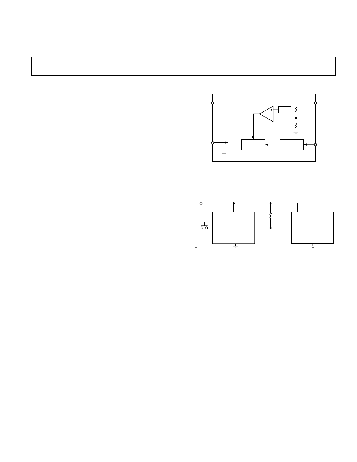
Open-Drain Microprocessor
V
REF
DEBOUNCE
RESET
CIRCUITRY
ADM6315
V
CC
MR
GND
RESET
a
FEATURES
Superior Upgrade for MAX6315
Specified Over Temperature
Low Power Consumption (5 A Typ)
Precision Voltage Monitor of Voltages from 2.5 V to
5 V at 100 mV Increments
Reset Assertion Down to V
Built-In Manual Reset
Pin Compatible with the ADM811
APPLICATIONS
Microprocessor Systems
Controllers
Intelligent Instruments
Automotive Systems
Safety Systems
Portable Instruments
GENERAL DESCRIPTION
CC
> 1 V
Supervisory Circuit in 4-Lead SOT-143
The ADM6315 is a reliable voltage monitoring device that is
suitable for use in most voltage monitoring applications.
The ADM6315 is designed to monitor as little as a 1.8% degradation of a power supply voltage. Voltages that can be monitored by the ADM6315 are all voltages (at 100 mV increments)
from 2.5 V to 5 V.
Included in this circuit is a debounced Manual Reset input.
Reset can be activated using an ordinary switch (pulling MR
low), by a low input from another digital device or by a degradation of the supply voltage. The manual reset function is very
useful, especially if the circuit in which the ADM6315 is operating, enters into a state that can only be detected by the user.
Allowing the user to manually reset a system can reduce the
damage or danger that could be otherwise caused by an out of
control or locked-up system.
The ADM6315 comes in a cost and space efficient SOT-143
package.
ADM6315
FUNCTIONAL BLOCK DIAGRAM
V
CC
10kV
MR
ADM6315
RESET
GND
Figure 1. Typical Operating Circuit
SYSTEM POWER
mP
SYSTEM
RESET
GND
REV. 0
Information furnished by Analog Devices is believed to be accurate and
reliable. However, no responsibility is assumed by Analog Devices for its
use, nor for any infringements of patents or other rights of third parties
which may result from its use. No license is granted by implication or
otherwise under any patent or patent rights of Analog Devices.
One Technology Way, P.O. Box 9106, Norwood, MA 02062-9106, U.S.A.
Tel: 781/329-4700 World Wide Web Site: http://www.analog.com
Fax: 781/326-8703 © Analog Devices, Inc., 1999

ADM6315–SPECIFICATIONS
P
arameter Min Typ Max Units Test Conditions/Comments
(VCC = Full Operating Range, TA = T
MIN
to T
, VCC Typ = 5 V unless otherwise noted)
MAX
SUPPLY
Operating Voltage 1.0 5.5 V T
Supply Current 5 12 µAV
V
CC
412 µAV
1
RESET VOLTAGE THRESHOLD (V
TH
)
V
– 1.8% V
TH
V
– 2.5% V
TH
TH
V
+ 1.8% V T
TH
+ 2.5% V T
TH
= 0°C to +70°C
A
= 5.5 V (No Load)
CC
= 3.6 V (No Load)
CC
= +25°C
A
= 0°C to +70°C
A
RESET THRESHOLD TEMPERATURE
COEFFICIENT 60 ppm/°C
V
TO RESET DELAY 35 µsV
CC
= Falling at 1 mV/µs
CC
RESET ACTIVE TIMEOUT PERIOD 1 1.4 2.6 ms ADM6315xxD1
20 28 53 ms ADM6315xxD2
140 200 370 ms ADM6315xxD3
1120 1570 2960 ms ADM6315xxD4
MANUAL RESET
Input Threshold 0.8 V VTH > 4.0 V (VIL)
0.3 V
CC
2.4 V V
VV
0.7 V
CC
VV
> 4.0 V (VIH)
TH
< 4.0 V (VIL)
TH
< 4.0 V (VIH)
TH
Minimum Input Pulse 1 µs
Glitch Rejection 100 ns
To Reset Delay 500 ns
Pull-Up Resistance 32 63 100 kΩ
RESET OUTPUT
Output Voltage 0.4 V VCC > 4.25 V, I
0.3 V V
0.3 V V
Output Leakage Current 1 µAV
NOTES
1
The ADM6315 is available with preset reset threshold values from 2.5 V to 5 V at 100 mV increments.
Specifications subject to change without notice.
> 2.5 V, I
CC
> 1 V, I
CC
> VTH, RESET Deasserted
CC
SINK
SINK
= 80 mA
SINK
= 3.2 mA
= 1.2 mA
–2–
REV. 0
ADM6315
ABSOLUTE MAXIMUM RATINGS*
(T
= +25°C unless otherwise noted)
A
Terminal Voltage (With Respect to Ground)
V
. . . . . . . . . . . . . . . . . . . . . . . . . . . . . . . –0.3 V to +6 V
CC
All Other Inputs . . . . . . . . . . . . . . . . .–0.3 V to V
+ 0.3 V
CC
Input Current
V
. . . . . . . . . . . . . . . . . . . . . . . . . . . . . . . . . . . . . 20 mA
CC
Output Current
RESET . . . . . . . . . . . . . . . . . . . . . . . . . . . . . . . . . . 20 mA
Power Dissipation (T
= +70°C)
A
RT-4, SOT-143
Derate by 4 mW/°C above +70°C . . . . . . . . . . . 320 mW
Thermal Impedance . . . . . . . . . . . . . . . . . . . . 330°C/W
θ
JA
Operating Temperature Range . . . . . . . . . . . –40°C to +85°C
Storage Temperature Range . . . . . . . . . . . . –65°C to +160°C
Lead Temperature (Soldering, 10 secs) . . . . . . . . . . . .+300°C
Vapor Phase (60 sec) . . . . . . . . . . . . . . . . . . . . . . . .+215°C
Infrared (15 sec) . . . . . . . . . . . . . . . . . . . . . . . . . . . .+220°C
ESD Rating . . . . . . . . . . . . . . . . . . . . . . . . . . . . . . . . . . 2.5 kV
*Stresses above those listed under Absolute Maximum Ratings may cause perma-
nent damage to the device. This is a stress rating only; functional operation of the
device at these or any other conditions above those listed in the operational
sections of this specification is not implied. Exposure to absolute maximum ratings
for extended periods of time may affect device reliability.
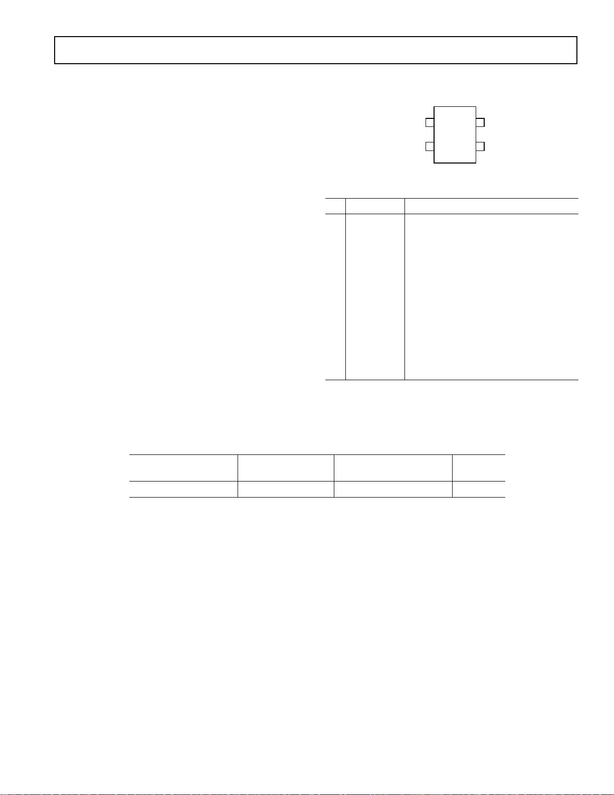
PIN CONFIGURATION
1
GND
ADM6315
TOP VIEW
(Not to Scale)
23
RESET
4
V
CC
MR
PIN FUNCTION DESCRIPTIONS
Pin Mnemonic Function
1 GND 0 V. Ground reference for all signals.
2 RESET Active Low Logic Output. RESET re-
mains low while V
is below the reset
CC
threshold or when MR is low, RESET
then remains low for either 1 ms (min),
20 ms (min), 140 ms (min) or 1120 ms
(min) after V
rises above the reset
CC
threshold and MR is high.
3 MR Manual Reset. This active low de-
bounced input will ignore input pulses of
100 ns (typical) and is guaranteed to
accept input pulses of greater than 1 µs.
Leave floating when not used.
4V
CC
Monitored supply voltage.
ORDERING GUIDE
Temperature Package Package
Model Range Description Option
ADM6315–xxxxxxx-xx* –40°C to +85°C Plastic Surface Mount SOT-143
*Refer to Tables I to IV.
REV. 0
–3–

ADM6315
–Typical Performance Characteristics
10
8
VCC = 5.5
6
– mA
DD
I
4
VCC = 3
2
0
–20 0 20 40 60 80 100 125
–40
VCC = 1
TEMPERATURE – 8C
Figure 2. Supply Current vs. Temperature
450
400
350
300
250
200
150
100
POWER-DOWN RESET DELAY – ms
50
0
–20 0 20 40 60 80 100 125
–40
TEMPERATURE – 8C
VOD = 20mV
VOD = 125mV
VOD = 200mV
Figure 3. Power-Down Reset Delay vs. Temperature
800
700
600
500
400
300
200
100
MAXIMUM TRANSIENT DURATION – ms
0
–100
0
4
8 20 60 100 400
RESET COMPARATOR OVERDRIVE, VTH-VCC – mV
Figure 5. Maximum Transient Duration vs.
800 1200 1600
RESET
Com-
parator Overdrive
1.005
1.000
0.995
NORMALIZED THRESHOLD – V
0.990
–20 0 20 40 60 80 100 125
–40
TEMPERATURE – 8C
Figure 6. Normalized Reset Threshold vs. Temperature
Falling)
(V
CC
1.06
1.04
1.02
1.00
0.98
0.96
NORMALIZED RESET TIMEOUT – ms
0.94
–20 0 20 40 60 80 100 125
–40
TEMPERATURE – 8C
Figure 4. Normalized Reset Timeout Period vs. Temperature (V
Rising)
CC
–4–
12
+858C
10
8
6
+258C
4
SUPPLY CURRENT – mA
2
0
0
1234
SUPPLY VOLTAGE – V
–408C
Figure 7. Supply Current vs. Supply Voltage
5
REV. 0

ADM6315
VCC TRIP-POINT (MIN)
V
CC
TRIP-POINT (MAX)
V
CC
TRIP-POINT
RESET ACTIVE TIMEOUT
RST
V
CC
INTERFACING TO OTHER DEVICES
OUTPUT
The ADM6315 series is designed to integrate with as many
devices as possible. One feature of the ADM6315 is the RESET
open drain output, which can sink current from sources with a
voltage greater than the V
of the ADM6315 input making it
CC
suitable for use in more diverse applications.
THE BENEFITS OF A VERY ACCURATE RESET
THRESHOLD
Because the ADM6315 series can operate effectively even when
there are large degradations of the supply voltages (due to an
accurate internal voltage reference circuit), the possibility of a
malfunction during a power failure is greatly reduced.
V
CC
VCC TRIP-POINT(MAX)
RST
VCC TRIP-POINT
V
TO RESET
CC
DELAY
VCC TRIP-POINT(MIN)
VOL
Figure 8. VCC Power-Down/Brownout Timing Diagram
DETAILED DESCRIPTION
The ADM6315 is designed to protect the integrity of a systems
operation by ensuring the proper operation of the system during
power-up, power-down and brownout conditions.
When the ADM6315 is powered-up (depending on the selected
reset active timeout), the RESET output of the ADM6315 will
remain low for a period typically equalling the Reset Active
Timeout Period. This is designed to give the system time to
power-up correctly and for the power supply to stabilize before
any devices are brought out of reset and allowed to begin executing instructions. Initializing a system in this way provides a
more reliable start-up for microprocessor systems.
When a brownout condition occurs (assuming V
is falling at
CC
1 mV/µs), the ADM6315 will produce a reset in typically 35 µs.
Producing a reset this fast means that the entire system can be
reset together before any part of the systems’ voltage falls below
its recommended operating voltage. This can avoid dangerous
and/or erroneous operation of a microprocessor-based system.
The MR input will (typical) ignore negative going pulses faster
than 100 ns and is guaranteed to accept any negative going
input pulse of a duration greater than or equal to 1 µs. If MR is
connected to long cables or used in a noisy environment, then
placing a 1 µF decoupling capacitor between the MR input and
ground will further improve the glitch immunity of the ADM6315.
Figure 9. VCC Power-Up Timing Diagram
TRANSIENT IMMUNITY
As well as being an accurate reset circuit, the ADM6315 has
good immunity to negative going transients (Figure 5). Because
of this characteristic, the ADM6315 is suitable for use in noisy
environments.
Figure 5 shows the reset comparator overdrive (the maximum
magnitude of negative going pulses with respect to the typical
reset threshold) versus pulse duration, without causing a reset.
MANUAL RESET INPUT
The ADM6315 also provides an additional input, MR. This
input can be used as either a means for the system operator to
manually reset the system via a switch or for a digital circuit to
reset the system.
REV. 0
–5–

ADM6315
Table I.
Min
Trip- Timeout
Model* Point (ms) Brand
ADM6315-50D1ART-RL7 5.00 1 MDZ
ADM6315-50D1ART-RL 5.00 1 MDZ
ADM6315-49D1ART-RL7 4.90 1 MDY
ADM6315-49D1ART-RL 4.90 1 MDY
ADM6315-48D1ART-RL7 4.80 1 MDX
ADM6315-48D1ART-RL 4.80 1 MDX
ADM6315-47D1ART-RL7 4.70 1 MDW
ADM6315-47D1ART-RL 4.70 1 MDW
ADM6315-46D1ART-RL7 4.63 1 MDV
ADM6315-46D1ART-RL 4.63 1 MDV
ADM6315-45D1ART-RL7 4.50 1 MDU
ADM6315-45D1ART-RL 4.50 1 MDU
ADM6315-44D1ART-RL7 4.39 1 MDT
ADM6315-44D1ART-RL 4.39 1 MDT
ADM6315-43D1ART-RL7 4.30 1 MDS
ADM6315-43D1ART-RL 4.30 1 MDS
ADM6315-42D1ART-RL7 4.20 1 MDR
ADM6315-42D1ART-RL 4.20 1 MDR
ADM6315-41D1ART-RL7 4.10 1 MDQ
ADM6315-41D1ART-RL 4.10 1 MDQ
ADM6315-40D1ART-RL7 4.00 1 MDP
ADM6315-40D1ART-RL 4.00 1 MDP
ADM6315-39D1ART-RL7 3.90 1 MDO
ADM6315-39D1ART-RL 3.90 1 MDO
ADM6315-38D1ART-RL7 3.80 1 MDN
ADM6315-38D1ART-RL 3.80 1 MDN
ADM6315-37D1ART-RL7 3.70 1 MDM
ADM6315-37D1ART-RL 3.70 1 MDM
ADM6315-36D1ART-RL7 3.60 1 MDL
ADM6315-36D1ART-RL 3.60 1 MDL
ADM6315-35D1ART-RL7 3.50 1 MDK
ADM6315-35D1ART-RL 3.50 1 MDK
ADM6315-34D1ART-RL7 3.40 1 MDJ
ADM6315-34D1ART-RL 3.40 1 MDJ
ADM6315-33D1ART-RL7 3.30 1 MDI
ADM6315-33D1ART-RL 3.30 1 MDI
ADM6315-32D1ART-RL7 3.20 1 MDH
ADM6315-32D1ART-RL 3.20 1 MDH
ADM6315-31D1ART-RL7 3.08 1 MDG
ADM6315-31D1ART-RL 3.08 1 MDG
ADM6315-30D1ART-RL7 3.00 1 MDF
ADM6315-30D1ART-RL 3.00 1 MDF
ADM6315-29D1ART-RL7 2.93 1 MDE
ADM6315-29D1ART-RL 2.93 1 MDE
ADM6315-28D1ART-RL7 2.80 1 MDD
ADM6315-28D1ART-RL 2.80 1 MDD
ADM6315-27D1ART-RL7 2.70 1 MDC
ADM6315-27D1ART-RL 2.70 1 MDC
ADM6315-26D1ART-RL7 2.63 1 MDB
ADM6315-26D1ART-RL 2.63 1 MDB
ADM6315-25D1ART-RL7 2.50 1 MDA
ADM6315-25D1ART-RL 2.50 1 MDA
NOTES
ADM6315-xxxxxxx-RL7 are in reels of 3,000 pieces.
ADM6315-xxxxxxx-RL are in reels of 10,000 pieces.
*Only available in reels.
Table II.
Min
Trip- Timeout
Model* Point (ms) Brand
ADM6315-50D2ART-RL7 5.00 20 MEZ
ADM6315-50D2ART-RL 5.00 20 MEZ
ADM6315-49D2ART-RL7 4.90 20 MEY
ADM6315-49D2ART-RL 4.90 20 MEY
ADM6315-48D2ART-RL7 4.80 20 MEX
ADM6315-48D2ART-RL 4.80 20 MEX
ADM6315-47D2ART-RL7 4.70 20 MEW
ADM6315-47D2ART-RL 4.70 20 MEW
ADM6315-46D2ART-RL7 4.63 20 MEV
ADM6315-46D2ART-RL 4.63 20 MEV
ADM6315-45D2ART-RL7 4.50 20 MEU
ADM6315-45D2ART-RL 4.50 20 MEU
ADM6315-44D2ART-RL7 4.39 20 MET
ADM6315-44D2ART-RL 4.39 20 MET
ADM6315-43D2ART-RL7 4.30 20 MES
ADM6315-43D2ART-RL 4.30 20 MES
ADM6315-42D2ART-RL7 4.20 20 MER
ADM6315-42D2ART-RL 4.20 20 MER
ADM6315-41D2ART-RL7 4.10 20 MEQ
ADM6315-41D2ART-RL 4.10 20 MEQ
ADM6315-40D2ART-RL7 4.00 20 MEP
ADM6315-40D2ART-RL 4.00 20 MEP
ADM6315-39D2ART-RL7 3.90 20 MEO
ADM6315-39D2ART-RL 3.90 20 MEO
ADM6315-38D2ART-RL7 3.80 20 MEN
ADM6315-38D2ART-RL 3.80 20 MEN
ADM6315-37D2ART-RL7 3.70 20 MEM
ADM6315-37D2ART-RL 3.70 20 MEM
ADM6315-36D2ART-RL7 3.60 20 MEL
ADM6315-36D2ART-RL 3.60 20 MEL
ADM6315-35D2ART-RL7 3.50 20 MEK
ADM6315-35D2ART-RL 3.50 20 MEK
ADM6315-34D2ART-RL7 3.40 20 MEJ
ADM6315-34D2ART-RL 3.40 20 MEJ
ADM6315-33D2ART-RL7 3.30 20 MEI
ADM6315-33D2ART-RL 3.30 20 MEI
ADM6315-32D2ART-RL7 3.20 20 MEH
ADM6315-32D2ART-RL 3.20 20 MEH
ADM6315-31D2ART-RL7 3.08 20 MEG
ADM6315-31D2ART-RL 3.08 20 MEG
ADM6315-30D2ART-RL7 3.00 20 MEF
ADM6315-30D2ART-RL 3.00 20 MEF
ADM6315-29D2ART-RL7 2.93 20 MEE
ADM6315-29D2ART-RL 2.93 20 MEE
ADM6315-28D2ART-RL7 2.80 20 MED
ADM6315-28D2ART-RL 2.80 20 MED
ADM6315-27D2ART-RL7 2.70 20 MEC
ADM6315-27D2ART-RL 2.70 20 MEC
ADM6315-26D2ART-RL7 2.63 20 MEB
ADM6315-26D2ART-RL 2.63 20 MEB
ADM6315-25D2ART-RL7 2.50 20 MEA
ADM6315-25D2ART-RL 2.50 20 MEA
–6–
REV. 0

ADM6315
Table III.
Min
Trip- Timeout
Model* Point (ms) Brand
ADM6315-50D3ART-RL7 5.00 140 MFZ
ADM6315-50D3ART-RL 5.00 140 MFZ
ADM6315-49D3ART-RL7 4.90 140 MFY
ADM6315-49D3ART-RL 4.90 140 MFY
ADM6315-48D3ART-RL7 4.80 140 MFX
ADM6315-48D3ART-RL 4.80 140 MFX
ADM6315-47D3ART-RL7 4.70 140 MFW
ADM6315-47D3ART-RL 4.70 140 MFW
ADM6315-46D3ART-RL7 4.63 140 MFV
ADM6315-46D3ART-RL 4.63 140 MFV
ADM6315-45D3ART-RL7 4.50 140 MFU
ADM6315-45D3ART-RL 4.50 140 MFU
ADM6315-44D3ART-RL7 4.39 140 MFT
ADM6315-44D3ART-RL 4.39 140 MFT
ADM6315-43D3ART-RL7 4.30 140 MFS
ADM6315-43D3ART-RL 4.30 140 MFS
ADM6315-42D3ART-RL7 4.20 140 MFR
ADM6315-42D3ART-RL 4.20 140 MFR
ADM6315-41D3ART-RL7 4.10 140 MFQ
ADM6315-41D3ART-RL 4.10 140 MFQ
ADM6315-40D3ART-RL7 4.00 140 MFP
ADM6315-40D3ART-RL 4.00 140 MFP
ADM6315-39D3ART-RL7 3.90 140 MFO
ADM6315-39D3ART-RL 3.90 140 MFO
ADM6315-38D3ART-RL7 3.80 140 MFN
ADM6315-38D3ART-RL 3.80 140 MFN
ADM6315-37D3ART-RL7 3.70 140 MFM
ADM6315-37D3ART-RL 3.70 140 MFM
ADM6315-36D3ART-RL7 3.60 140 MFL
ADM6315-36D3ART-RL 3.60 140 MFL
ADM6315-35D3ART-RL7 3.50 140 MFK
ADM6315-35D3ART-RL 3.50 140 MFK
ADM6315-34D3ART-RL7 3.40 140 MFJ
ADM6315-34D3ART-RL 3.40 140 MFJ
ADM6315-33D3ART-RL7 3.30 140 MFI
ADM6315-33D3ART-RL 3.30 140 MFI
ADM6315-32D3ART-RL7 3.20 140 MFH
ADM6315-32D3ART-RL 3.20 140 MFH
ADM6315-31D3ART-RL7 3.08 140 MFG
ADM6315-31D3ART-RL 3.08 140 MFG
ADM6315-30D3ART-RL7 3.00 140 MFF
ADM6315-30D3ART-RL 3.00 140 MFF
ADM6315-29D3ART-RL7 2.93 140 MFE
ADM6315-29D3ART-RL 2.93 140 MFE
ADM6315-28D3ART-RL7 2.80 140 MFD
ADM6315-28D3ART-RL 2.80 140 MFD
ADM6315-27D3ART-RL7 2.70 140 MFC
ADM6315-27D3ART-RL 2.70 140 MFC
ADM6315-26D3ART-RL7 2.63 140 MFB
ADM6315-26D3ART-RL 2.63 140 MFB
ADM6315-25D3ART-RL7 2.50 140 MFA
ADM6315-25D3ART-RL 2.50 140 MFA
NOTES
All parts in bold are ex-stock. Consult factory for availability of orders.
ADM6315-xxxxxxx-RL7 are in reels of 3,000 pieces.
ADM6315-xxxxxxx-RL are in reels of 10,000 pieces.
*Only available in reels.
Table IV.
Min
Trip- Timeout
Model* Point (ms) Brand
ADM6315-50D4ART-RL 5.00 1120 MGZ
ADM6315-50D4ART-RL7 5.00 1120 MGZ
ADM6315-49D4ART-RL 4.90 1120 MGY
ADM6315-49D4ART-RL7 4.90 1120 MGY
ADM6315-48D4ART-RL 4.80 1120 MGX
ADM6315-48D4ART-RL7 4.80 1120 MGX
ADM6315-47D4ART-RL 4.70 1120 MGW
ADM6315-47D4ART-RL7 4.70 1120 MGW
ADM6315-46D4ART-RL 4.63 1120 MGV
ADM6315-46D4ART-RL7 4.63 1120 MGV
ADM6315-45D4ART-RL 4.50 1120 MGU
ADM6315-45D4ART-RL7 4.50 1120 MGU
ADM6315-44D4ART-RL 4.39 1120 MGT
ADM6315-44D4ART-RL7 4.39 1120 MGT
ADM6315-43D4ART-RL 4.30 1120 MGS
ADM6315-43D4ART-RL7 4.30 1120 MGS
ADM6315-42D4ART-RL 4.20 1120 MGR
ADM6315-42D4ART-RL7 4.20 1120 MGR
ADM6315-41D4ART-RL 4.10 1120 MGQ
ADM6315-41D4ART-RL7 4.10 1120 MGQ
ADM6315-40D4ART-RL 4.00 1120 MGP
ADM6315-40D4ART-RL7 4.00 1120 MGP
ADM6315-39D4ART-RL 3.90 1120 MGO
ADM6315-39D4ART-RL7 3.90 1120 MGO
ADM6315-38D4ART-RL 3.80 1120 MGN
ADM6315-38D4ART-RL7 3.80 1120 MGN
ADM6315-37D4ART-RL 3.70 1120 MGM
ADM6315-37D4ART-RL7 3.70 1120 MGM
ADM6315-36D4ART-RL 3.60 1120 MGL
ADM6315-36D4ART-RL7 3.60 1120 MGL
ADM6315-35D4ART-RL 3.50 1120 MGK
ADM6315-35D4ART-RL7 3.50 1120 MGK
ADM6315-34D4ART-RL 3.40 1120 MGJ
ADM6315-34D4ART-RL7 3.40 1120 MGJ
ADM6315-33D4ART-RL 3.30 1120 MGI
ADM6315-33D4ART-RL7 3.30 1120 MGI
ADM6315-32D4ART-RL 3.20 1120 MGH
ADM6315-32D4ART-RL7 3.20 1120 MGH
ADM6315-31D4ART-RL 3.08 1120 MGG
ADM6315-31D4ART-RL7 3.08 1120 MGG
ADM6315-30D4ART-RL 3.00 1120 MGF
ADM6315-30D4ART-RL7 3.00 1120 MGF
ADM6315-29D4ART-RL 2.93 1120 MGE
ADM6315-29D4ART-RL7 2.93 1120 MGE
ADM6315-28D4ART-RL 2.80 1120 MGD
ADM6315-28D4ART-RL7 2.80 1120 MGD
ADM6315-27D4ART-RL 2.70 1120 MGC
ADM6315-27D4ART-RL7 2.70 1120 MGC
ADM6315-26D4ART-RL 2.63 1120 MGB
ADM6315-26D4ART-RL7 2.63 1120 MGB
ADM6315-25D4ART-RL 2.50 1120 MGA
ADM6315-25D4ART-RL7 2.50 1120 MGA
REV. 0
–7–

ADM6315
OUTLINE DIMENSIONS
Dimensions shown in inches and (mm).
4-Lead Plastic Surface Mount Package
(SOT-143)
0.079 (2.00)
0.071 (1.80)
0.055 (1.40)
0.047 (1.20)
PIN 1
78
0.004 (0.10)
0.001 (0.03)
SEATING
PLANE
4
1 2
0.080 (2.03)
0.070 (1.78)
0.120 (3.05)
0.105 (2.67)
0.037 (0.94)
0.030 (0.77)
3
0.021 (0.54)
0.015 (0.38)
0.098 (2.50)
0.083 (2.10)
0.040 (1.02)
0.031 (0.79)
0.0059 (0.089)
0.0035 (0.15)
0.010 (0.25)
0.005 (0.13)
C3460–8–3/99
88
08
–8–
PRINTED IN U.S.A.
REV. 0
 Loading...