

Supervisory ICs
ADM6305/ADM6306
Rev. A
Information furnished by Analog Devices is believed to be accurate and reliable. However, no
Trademarks and registered trademarks are the property of their respective owners.
Fax: 781.461.3113 ©2010–2012 Analog Devices, Inc. All rights reserved.
RESET
GENERATOR
RESET
0.4V/1.23V
RST IN1
V
CC
GND
0.4V/1.23V
RST IN2
ADM6305
09345-001
RESET
GENERATOR
GLITCH
REJECTION
RESET
1.23V
GND
0.4V/1.23V
RST IN
MR
ADM6306
V
CC
V
CC
09345-002
Data Sheet
FEATURES
Adjustable input threshold voltage options: 0.4 V and 1.23 V
Pre-trimmed V
Increments between 2.5 V and 5 V
Manual reset input (ADM6306)
4 factory programmed reset timeout delays
1 ms, 20 ms, 140 ms, and 1.12 sec (minimum)
Reset output stage: active low, open drain
Low power consumption: 5 µA typical
Power supply glitch immunity
5-lead SOT-23 package
Temperature range: −40°C to +125°C
APPLICATIONS
Portable/battery-operated equipment
Microprocessor systems
Multivoltage applications
threshold options (ADM6306)
CC
Multiple Input Programmable
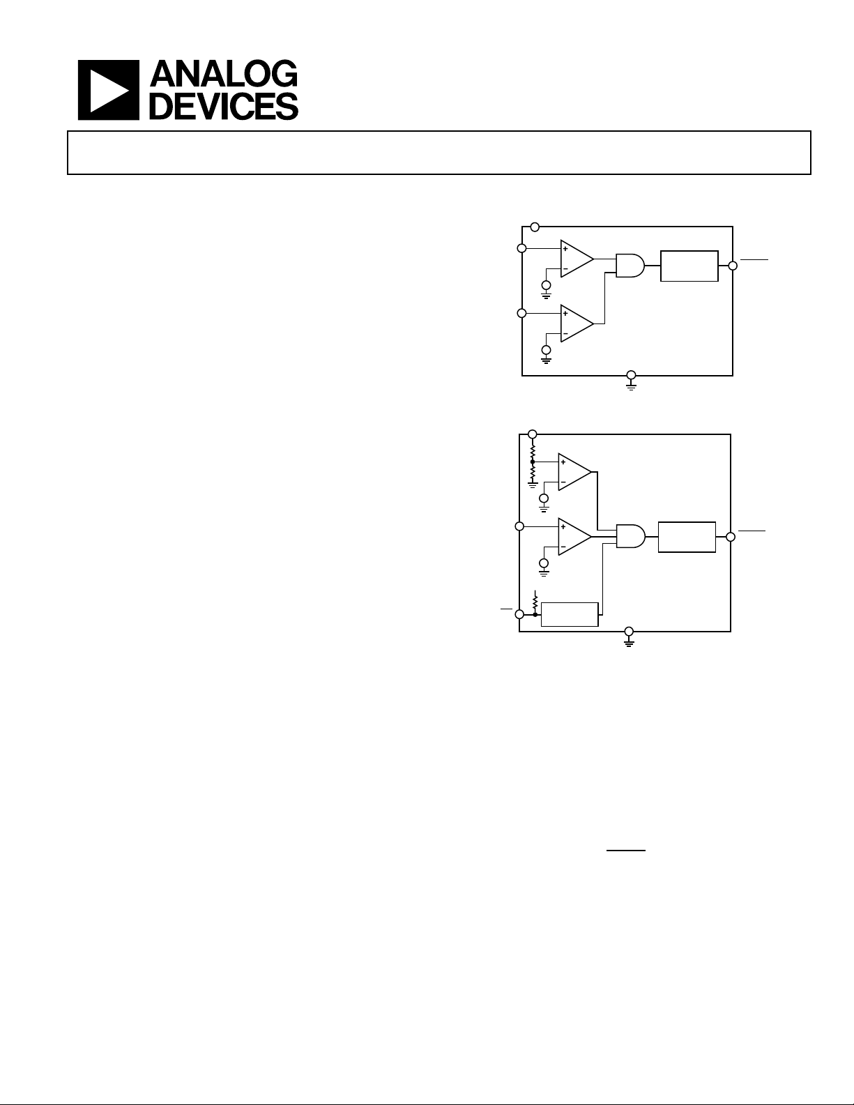
FUNCTIONAL BLOCK DIAGRAMS
Figure 1.
GENERAL DESCRIPTION
The ADM6305/ADM6306 are dual voltage supervisors
designed to monitor two supplies and provide a reset signal to
DSP- and microprocessor-based systems. Low supply current
and a small form factor make these devices suitable for portable
and battery-operated applications.
If a monitored power supply voltage falls below the minimum
voltage threshold, a single active low output asserts triggering a
system reset. Once all voltages rise above the selected threshold
level, the reset signal remains low for the reset timeout period.
Four reset timeout options are available.
The ADM6305 monitors two supplies via two adjustable
resistor-programmable undervoltage reset inputs. Both RST
IN1 and RST IN2 have a reset threshold of either 0.4 V or
1.23 V depending on the particular model; that is, the RST IN1
and RST IN2 threshold of the ADM6305DxARJZ model is
responsibility is assumed by Analog Devices for its use, nor for any infringements of patents or other
rights of third parties that may result from its use. Specifications subject to change without n otice. No
license is granted by implication or otherwise under any patent or patent rights of Analog Devices.
Figure 2.
1.23 V, while in the case of ADM6305DxARJZ1 model, it is
0.4 V. The V
input of the ADM6305 is not a monitored input.
CC
The ADM6306 has one adjustable undervoltage reset input,
RST IN, which features a choice of reset threshold, 0.4 V or
1.23 V (see the Ordering Guide for more information). The
ADM6306 incorporates a variety of internally pretrimmed V
undervoltage threshold options for monitoring supply voltages
in increments between 2.5 V and 5 V. The ADM6306 also
includes a manual reset input.
The ADM6305/ADM6306
as V
exceeds 0.9 V.
CC
RESET
output remains valid as long
The ADM6305/ADM6306 are available in a 5-lead SOT-23
package. These devices are specified over the temperature range
of −40°C to +125°C.
One Technology Way, P.O. Box 9106, Norwood, MA 02062-9106, U.S.A.
Tel: 781.329.4700
www.analog.com
CC

ADM6305/ADM6306 Data Sheet
TABLE OF CONTENTS
Features .............................................................................................. 1
Applications ....................................................................................... 1
Functional Block Diagrams ............................................................. 1
General Description ......................................................................... 1
Revision History ............................................................................... 2
Specifications ..................................................................................... 3
Absolute Maximum Ratings ............................................................ 4
Thermal Resistance ...................................................................... 4
ESD Caution .................................................................................. 4
REVISION HISTORY
4/12—Rev. 0 to Rev. A
Changes to Figure 1 and Figure 2 ................................................... 1
Change to V
Changes to Table 9 .......................................................................... 10
Updated Outline Dimensions ....................................................... 11
Changes to Ordering Guide .......................................................... 11
10/10—Revision 0: Initial Version
Pin Description, Tabl e 5 ........................................ 5
CC
Pin Configurations and Function Descriptions ............................5
Typical Performance Characteristics ..............................................6
Theory of Operation .........................................................................8
Input Configuration ......................................................................8
Reset Output Configuration ........................................................8
Manual Reset ..................................................................................8
Options ...............................................................................................9
Outline Dimensions ....................................................................... 11
Ordering Guide .......................................................................... 11
Rev. A | Page 2 of 12
Data Sheet ADM6305/ADM6306
1
0.9 V VCC that guarantees valid output
ADM630xD1
1.0
1.4
2.0
ms
ADM630xD4
1120
1570
2240
ms
SINK
SINK
RSTH
RST IN
RSTH
0.4 V ADJUSTABLE RESET COMPARTOR INPUT
RST INx
SPECIFICATIONS
VCC = 2.5 V to 5 V for the ADM6305, VCC = (VTH + 2.5%) to 5.5 V for the ADM6306. TA = −40°C to +125°C, unless otherwise noted.
Typ i cal values are at T
Table 1.
Parameter Min Typ Max Unit Test Conditions/Comments
OPERATING VOLTAGE RANGE, V
INPUT CURRENT, ICC 5 16 µA VCC = 5.5 V, TA = −40°C to +85°C
5 20 µA VCC = 5.5 V, TA = −40°C to +125°C
VCC THRESHOLD VOLTAGE (ADM6306)2 VTH − 1% VTH VTH + 1% V TA = 25°C
VTH − 1.5% VTH VTH + 1.5% V TA = −40°C to +85°C
VTH − 2.5% VTH VTH + 2.5% V TA = −40°C to +125°C
RESET THRESHOLD TEMPERATURE COEFFICIENT 25 ppm/°C
RESET THRESHOLD HYSTERESIS (V
RESET
TIMEOUT PERIOD (tRP)
ADM630xD2 20 28 40 ms
ADM630xD3 140 200 280 ms
= 25°C.
A
0.9 5.5 V
CC
) 2 × V
HYST
mV
TH
RESET
OUTPUT VOLTAGE (VOL)
0.3 V VCC > 2.5 V, I
0.3 V VCC > 1.2 V, I
0.3 V VCC > 1 V, I
0.3 V VCC > 0.9 V, I
MR
INPUT (ADM6306)
0.4 V
V
> 4.25 V, I
CC
= 3.2 mA
SINK
= 1.2 mA
SINK
= 500 μA
= 50 μA
= 25 μA
SINK
VIL 0.8 V VTH > 4.0 V
0.3 × VCC V VTH < 4.0 V
VIH 2.4 V VTH > 4.0 V
0.7 × VCC V VTH < 4.0 V
MR
Minimum Input Pulse Width
1 µs T
= 0°C to +70°C
A
1.5 µs TA = −40°C to +125°C
MR
Glitch Rejection
MR
To Reset Delay
MR
Pull-Up Resistance
0.1 µs
500 ns
32 63.5 100 kΩ
1.23 V ADJUSTABLE RESET COMPARATOR INPUT
RST INx Input Threshold, V
1.22 1.23 1.24 V TA = 25°C
1.211 1.23 1.249 TA = −40°C to +85°C
1.20 1.26 V TA = −40°C to +125°C
RST INx Input Current, I
−25 +25 nA V
−25 +25 nA 0 V < V
RST INx
< VCC – 0.3 V3, TA = −40°C to +85°C
RST IN
= V
RST INx Hysteresis 2.5 mV
RST INx Input Threshold, V
0.396 0.40 0.404 V TA = 25°C
RSTH
0.394 0.40 0.406 V TA = −40°C to +85°C
0.39 0.40 0.41 V TA = −40°C to +125°C
RST INx Input Current, I
−25 +25 nA V
1
The ADM6305 switches from undervoltage reset to normal operation when 1.5 V > VCC < 2.5 V.
2
The AMD6306 monitors VCC through an internal factory trimmed voltage divider, which programs the nominal reset threshold. Factory-trimmed reset thresholds are
available in approximately 100 mV increments from 2.5 V to 5 V.
3
Guaranteed by design.
−25 +25 nA
RST INx
0 V < V
RST IN
< VCC – 0.3 V3, TA = −40°C to +85°C
= V
RSTH
Rev. A | Page 3 of 12
ADM6305/ADM6306 Data Sheet
All Pins (Except VCC)
−0.3 V to (VCC + 0.3 V)
ABSOLUTE MAXIMUM RATINGS
Table 2.
Parameter Rating
VCC −0.3 V to +6 V
Input/Output Current 20 mA
Rate of Rise, VCC 100 V/µs
Storage Temperature Range −65°C to +160°C
Operating Temperature Range −40°C to +125°C
Lead Temperature (10 sec) 300°C
Junction Temperature 150°C
THERMAL RESISTANCE
Table 3.
Package Type θJA Unit
5-Lead SOT-23 240 °C/W
ESD CAUTION
Stresses above those listed under Absolute Maximum Ratings
may cause permanent damage to the device. This is a stress
rating only and functional operation of the device at these or
any other conditions above those indicated in the operational
section of this specification is not implied. Exposure to absolute
maximum rating conditions for extended periods may affect
device reliability.
Rev. A | Page 4 of 12

Data Sheet ADM6305/ADM6306
impedance allows the use of an external resistor divider to program the monitoring threshold. Connect this pin to
resistor divider to program the monitoring threshold. Connect this pin to
external resistor divider to program the monitoring threshold. Connect this pin to
RESET
1
RST IN1
3
GND
2
V
CC
5
RST IN2
3
ADM6305
TOP VIEW
(Not to Scale)
09345-003
RESET
1
MR
3
GND
2
V
CC
5
RST IN
3
ADM6306
TOP VIEW
(Not to Scale)
09345-004
PIN CONFIGURATIONS AND FUNCTION DESCRIPTIONS
Figure 3. ADM6305 Pin Configuration
Table 4. ADM6305 Pin Function Descriptions
Pin No. Mnemonic Description
1
Active Low, Open-Drain
RESET
RESET
Output.
2 GND Ground.
3 RST IN1 Adjustable Reset Comparator Input. This pin asserts
RESET
VCC if it is not used.
4 RST IN2 Adjustable Reset Comparator Input. This pin asserts
RESET
impedance allows the use of an external
VCC if it is not used.
5 VCC Power Supply Input. VCC is not monitored on the ADM6305.
Figure 4. ADM6306 Pin Configuration
Table 5. ADM6306 Pin Function Descriptions
Pin No. Mnemonic Description
1
Active Low, Open-Drain
RESET
RESET
Output.
2 GND Ground.
3
4 RST IN Adjustable Reset Comparator Input. This pin asserts
Manual Reset Input.
MR
RESET
impedance allows the use of an
VCC if it is not used.
5 VCC Power Supply Input. VCC is monitored on the ADM6306.
if the input voltage is below threshold. Its high input
if the input voltage is below threshold. Its high input
if the input voltage is below threshold. Its high input
Rev. A | Page 5 of 12

ADM6305/ADM6306 Data Sheet
6.0
3.0
3.5
4.0
4.5
5.0
5.5
–40 –20 0 20 40 60 80 100 120 125
SUPPLY CURRENT (µA)
TEMPERATURE (°C)
V
CC
= 2.5V
V
CC
= 3.5V
V
CC
= 4.5V
V
CC
= 5.5V
09345-005
1.10
0.85
0.90
0.95
1.00
1.05
–40 –20 0 20 40 60 80 100 120 125
NORMALIZED RESET TIMEOUT
TEMPERATURE (°C)
09345-006
1.010
0.990
0.992
0.994
0.996
0.998
1.000
1.002
1.004
1.006
1.008
–40 –20 0 20 40 60 80 100 120 125
NORMALIZED RESET THRESHOLD (V/V)
TEMPERATURE (°C)
09345-007
90
80
70
60
50
40
30
20
10
0
–40 –20 0 20 40 60 80 100 120 125
PROPAGAT ION DELAY (µs)
TEMPERATURE (°C)
1mV/1µs
10mV/1µs
09345-008
10k
1k
100
10
1
0 400 800 1200
TRANSIENT DURATION (µs)
OVERDRIVE, VTH – V
CC
(mV)
TRANSIENT DURATION
(µs) V
TH
= 5V
TRANSIENT DURATION
(µs) V
TH
= 2.5V
09345-009
09345-010
120
0
20
40
60
80
100
–40 –20 0 20 40 60 80 100 120 125
PROPAGAT ION DELAY (µs)
TEMPERATURE (°C)
1mV/1µs
10mV/1µs
TYPICAL PERFORMANCE CHARACTERISTICS
Figure 5. Supply Current vs. Temperature
Figure 6. Reset Timeout vs. Temperature
Figure 8. VCC Falling Propagation Delay vs. Temperature
Figure 9. Maximum Transient Duration vs. VCC Reset Threshold Overdrive
Figure 7. Reset Threshold vs. Temperature
Figure 10. RST IN(VTH = 1.23 V) Falling Propagation Delay vs. Temperature
Rev. A | Page 6 of 12

Data Sheet ADM6305/ADM6306
10k
1k
100
10
1
0 12001000800600400200
TRANSIENT DURATION (µs)
OVERDRIVE, V
REF
– V
RST IN
(mV)
TRANSIENT DURATION
(µs) 5V
TRANSIENT DURATION
(µs) 3V
09345-011
120
0
20
40
60
80
100
–40 –20 0 20 40 60 80 100 120 125
RST INx PRO P AGATION DELAY (µs)
TEMPERATURE (°C)
1mV/1µs
10mV/1µs
09345-012
10k
1k
100
10
1
0
100 200 300
TRANSIENT DURATION (µs)
OVERDRIVE, V
REF
– V
RST IN
(mV)
TRANSIENT DURATION
(µs) 5V
TRANSIENT DURATION
(µs) 3V
09345-013
Figure 11. Maximum Transient Duration vs. RST IN (VTH = 1.23 V) Threshold
Overdrive
Figure 12. RST INx (VTH = 0.4 V) Falling Propagation Delay vs. Temperature
Figure 13. Maximum Transient Duration vs. RST INx (VTH = 0.4 V) Threshold
Overdrive
Rev. A | Page 7 of 12

ADM6305/ADM6306 Data Sheet
V
THEORY OF OPERATION
The ADM6305/ADM6306 are compact, low power supervisory
circuits capable of monitoring two voltage rails. If a monitored
voltage drops below its associated threshold, the active low reset
output asserts low.
The ADM6305 monitors two supplies via two adjustable
resistor-programmable undervoltage reset inputs. Both RST
IN1 and RST IN2 have a reset threshold of either 0.4 V or
1.23 V depending on the particular model; that is, the RST
IN1 and RST IN2 threshold of the ADM6305DxARJZ model
is 1.23 V, while in the case of ADM6305DxARJZ1 model, it is
0.4 V. The V
input of the ADM6305 is not a monitored input.
CC
The ADM6306 has one adjustable undervoltage reset input,
RST IN, which features a choice of reset threshold, 0.4 V or
1.23 V (see the Ordering Guide for more information). The
ADM6306 incorporates a variety of internally pretrimmed V
CC
undervoltage threshold options for monitoring supply voltages
in increments between 2.5 V to 5 V. The ADM6306 also
includes a manual reset input.
INPUT CONFIGURATION
The threshold voltage at an adjustable input is either 0.4 V or
1.23 V. To monitor a voltage greater than the typical adjustable
threshold, V
circuit as depicted in Figure 14, where
, connect a resistor divider network to the
RSTH
R2R1
R2
IN
R1
R2
VV
RSTHTH
on this input. The ADM6305/ADM6306 are powered via V
Figure 9 shows the maximum transient duration vs. V
threshold overdrive, for which reset pulses are not generated.
Figure 9 depicts the maximum pulse width that a negative going
V
transient may typically have without causing
CC
RESET
asserted. As the amplitude of the transient increases, the
maximum allowable pulse width decreases. The addition of a
bypass capacitor on V
provides additional transient immunity.
CC
RESET OUTPUT CONFIGURATION
The ADM6305/ADM6306 are available in a choice of four
reset timeouts. Once the monitored supplies rise above their
associated threshold level, the
the reset timeout period before deasserting. Subsequently, if
a monitored supply falls below its associated threshold, the
RESET
output reasserts. The open-drain
ADM6305/ADM6306 remains valid as long as V
The ADM6305 remains in UVLO when V
RESET
output is controlled by RTS INx if VCC exceeds 2.5 V.
The open-drain
RESET
ADM6306 to interface easily with microprocessors and
devices with bidirectional reset pins. Connecting the supervisory devices
RESET
RESET
output directly to the microcontrollers
pin with a single pull-up resistor allows either device
to issue a system reset (see Figure 15).
V
CC
ADM6305/
ADM6306
RESET
RESET
signal remains low for
RESET
output of the
exceeds 0.9 V.
CC
is below 1.5 V. The
CC
output allows the ADM6305 and
R
PULL-UP
MICROPROCESSOR
RESET
CC
CC
reset
to be
.
V
RSTH
Figure 14. Setting the Adjustable Monitor
09345-014
The high input impedance (leakage of ±25 nA) of the adjustable
inputs minimizes the offset error caused by the leakage current
and external resistor divider. This allows the user to apply a divider
with large resistance to minimize the loss. The offset voltage
caused by the leakage current is calculated by R1 × ±25 nA.
The RST INx inputs are designed to ignore fast voltage
transients (see Figure 11 and Figure 12). Increase the noise
immunity by connecting a 0.1 µF bypass capacitor between
RST INx and ground. Note that adding capacitance to RST
INx slows the overall response time of the device.
There is no hysteresis associated with the 0.4 V adjustable
inputs; instead, a time-based glitch filter to prevent false
triggering is used. The glitch filter avoids the need to use a
portion of the operating supply range to provide hysteresis
Rev. A | Page 8 of 12
09345-015
Figure 15. Interfacing to Microprocessors with Bidirectional
RESET
Output
MANUAL RESET
The ADM6306 features a manual reset input (MR) which, when
MR
driven low, asserts the reset output. When
low to high, reset remains asserted for the duration of the reset
active timeout period before deasserting. The
63.5 k internal pull-up resistor so that the input is always
high when unconnected. An external push-button switch can
be connected between
MR
and ground so that the user can
generate a reset. Debounce circuitry is integrated on-chip for
this purpose. Noise immunity is provided on the
and fast, negative-going transients of up to 0.1 µs (typical) are
ignored. If required, a 0.1 F capacitor between
provides additional noise immunity.
transitions from
MR
input has a
MR
input,
MR
and ground

Data Sheet ADM6305/ADM6306
27
2.66
2.7
2.741
2.633
2.768
V
32
3.152
3.2
3.248
3.12
3.28
V
33
3.251
3.3
3.35
3.218
3.383
V
44
4.314
4.38
4.446
4.27
4.49
V
ADM630xD1
1.0
1.4
2.0
ms
Model
RST IN1
RST IN2
RST IN
OPTIONS
Table 6. ADM6306 VCC Reset Voltage Threshold Options
TA = 25°C TA= −40°C to +125°C
Reset Threshold Number
25 2.463 2.5 2.538 2.438 2.563 V
26 2.591 2.63 2.669 2.564 2.696 V
28 2.758 2.8 2.842 2.73 2.87 V
29 2.886 2.93 2.974 2.857 3 V
30 2.955 3 3.045 2.925 3.075 V
31 3.034 3.08 3.126 3.003 3.157 V
34 3.349 3.4 3.451 3.315 3.485 V
35 3.448 3.5 3.553 3.413 3.588 V
36 3.546 3.6 3.654 3.51 3.69 V
37 3.645 3.7 3.756 3.608 3.793 V
38 3.743 3.8 3.857 3.705 3.895 V
39 3.842 3.9 3.959 3.803 3.998 V
40 3.94 4 4.06 3.9 4.1 V
41 4.039 4.1 4.162 3.998 4.203 V
42 4.137 4.2 4.263 4.095 4.305 V
43 4.236 4.3 4.365 4.193 4.408 V
Unit Min Typ Max Min Max
45 4.433 4.5 4.568 4.388 4.613 V
46 4.561 4.63 4.699 4.514 4.746 V
47 4.63 4.7 4.771 4.583 4.818 V
48 4.728 4.8 4.872 4.68 4.92 V
49 4.827 4.9 4.974 4.778 5.023 V
50 4.925 5.0 5.075 4.875 5.125 V
Table 7. Reset Timeout Options
TA= −40°C to +125°C
Reset Timeout Period Code
ADM630xD2 20 28 40 ms
ADM630xD3 140 200 280 ms
ADM630xD4 1120 1570 2240 ms
Unit Min Typ Max
Table 8. Adjustable Input Threshold Options
ADM6305_ _ _ _ _Z-RL7 1.23 V 1.23 V N/A
ADM6305_ _ _ _ _Z1-RL7 0.4 V 0.4 V N/A
ADM6306_ _ _ _ _ _ _Z-R7 N/A N/A 1.23 V
ADM6306_ _ _ _ _ _ _Z1-R7 N/A N/A 0.4 V
Monitored Input Threshold
Rev. A | Page 9 of 12

ADM6305/ADM6306 Data Sheet
ADM6305D_ARJZ_-RL7
PACKING MATERI AL
RL7 = 7” TAPE & REEL
(3000 PIECE Q UANT ITY)
RST IN1 & RST IN2 ADJUSTABLE THRESHOLD
1:0.4V & 0.4V
BLANK: 1.23V & 1. 23V
Z = LEAD-FREE
PACKING MATERI AL
R7 = 7” TAPE & REE L
(3000 PIECE QUANTITY)
RST IN ADJUSTABLE THRESHOLD
1:0.4V
DASH: 1.23V
Z = LEAD-FREE
09345-017
Minimum Reset Timeout
09345-016
Table 9. Standard Models
Model
ADM6305D3ARJZ-RL7
ADM6305D3ARJZ1-RL7
ADM6306D131ARJZ-R7
ADM6306D131ARJZ1R7
ADM6306D329ARJZ-R7
ADM6306D330ARJZ-R7
ADM6306D331ARJZ-R7
ADM6306D344ARJZ-R7
ADM6306D346ARJZ-R7
RESET TIMEOUT PERIOD CODE (1 TO 4)
TEMPERATURE RANG E
A: –40°C TO + 125°C
PACKAGE DESIG NAT OR
RJ = SOT-23
Figure 16. ADM6305 Ordering Code Structure
ADM6306D_ _ _ARJZ_R7
RESET TIMEOUT (1 TO 4)
RESET THRES HOLD NUMBER
(SEE TABLE 6)
TEMPERATURE RANGE
A: –40°C TO + 125°C
PACKAGE DESIG NATOR
RJ = SOT-23
Figure 17. ADM6306 Ordering Code Structure
Monitored Input Threshold
RST IN1 RST IN2 VCC Reset RST IN
1.23 V 1.23 V N/A N/A 140 ms
0.4 V 0.4 V N/A N/A 140 ms
N/A N/A 3.08 V 1.23 V 1 ms
N/A N/A 3.08 V 0.4 V 1 ms
N/A N/A 2.93 V 1.23 V 140 ms
N/A N/A 3 V 1.23 V 140 ms
N/A N/A 3.08 V 1.23 V 140 ms
N/A N/A 4.38V 1.23 V 140 ms
N/A N/A 4.63 V 1.23 V 140 ms
Rev. A | Page 10 of 12

Data Sheet ADM6305/ADM6306
0
0
OUTLINE DIMENSIONS
3.00
2.90
2.80
1.30
1.15
0.90
.15 MAX
.05 MIN
1.70
1.60
1.50
5
123
4
1.90
BSC
0.50 MAX
0.35 MIN
COMPLIANT TO JEDEC STANDARDS MO-178-AA
0.95 BSC
1.45 MAX
0.95 MIN
3.00
2.80
2.60
SEATING
PLANE
0.20 MAX
0.08 MIN
10°
5°
0°
0.60
BSC
0.55
0.45
0.35
11-01-2010-A
Figure 18. 5-Lead Small Outline Transistor Package [SOT-23]
(RJ-5)
Dimensions shown in millimeters
ROUND SPROCKET HOLES
PIN 1 MARK ER
DIRECTION OF FEED
09345-019
Figure 19. ADM6305/ADM6306 Reel Orientation
ORDERING GUIDE
1, 2, 3
Model
ADM6305D3ARJZ-RL7 −40°C to +125°C 3,000 5-Lead SOT-23 RJ-5 LG9
ADM6305D3ARJZ1-RL7 −40°C to +125°C 3,000 5-Lead SOT-23 RJ-5 LG8
ADM6306D131ARJZ-R7 −40°C to +125°C 3,000 5-Lead SOT-23 RJ-5 LGA
ADM6306D131ARJZ1R7 −40°C to +125°C 3,000 5-Lead SOT-23 RJ-5 LGC
ADM6306D329ARJZ-R7 −40°C to +125°C 3,000 5-Lead SOT-23 RJ-5
ADM6306D330ARJZ-R7 −40°C to +125°C 3,000 5-Lead SOT-23 RJ-5
ADM6306D331ARJZ-R7 −40°C to +125°C 3,000 5-Lead SOT-23 RJ-5 LG6
ADM6306D344ARJZ-R7 −40°C to +125°C 3,000 5-Lead SOT-23 RJ-5
ADM6306D346ARJZ-R7 −40°C to +125°C 3,000 5-Lead SOT-23 RJ-5
1
ADM6305 and ADM6306 follow the C2 Pin 1 orientation standard for tape and reel packaging (see Figure 19).
2
If ordering nonstandard models, complete the ordering code shown in Figure 16 and Figure 17 by inserting the reset threshold, reset timeout, and adjustable
threshold suffixes. Contact Sales for availability of nonstandard models, quoting ADM6305-NTSD or ADM6306-NTSD first, and then the complete ordering code.
3
Z = RoHS Compliant Part.
4
A minimum of 10,000 must be ordered for nonstandard models.
Temperature Range Ordering Quantity4 Package Description Package Option Branding
LLY
LM0
LM1
LLZ
Rev. A | Page 11 of 12

ADM6305/ADM6306 Data Sheet
©2010–2012 Analog Devices, Inc. All rights reserved. Trademarks and
NOTES
registered trademarks are the property of their respective owners.
D09345-0-4/12(A)
Rev. A | Page 12 of 12
 Loading...