One Technology Way, P.O. Box 9106, Norwood. MA 02062-9106, U.S.A.
Tel: 617/329-4700 Fax: 617/326-8703
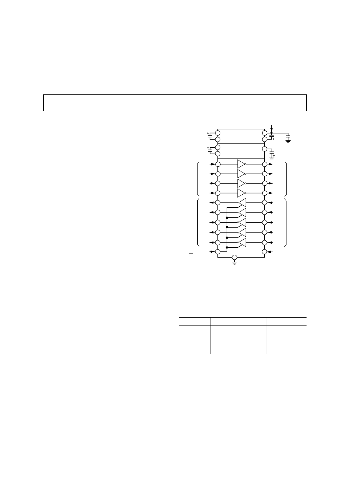
FUNCTIONAL BLOCK DIAGRAM
REV. 0
Information furnished by Analog Devices is believed to be accurate and
reliable. However, no responsibility is assumed by Analog Devices for its
use, nor for any infringements of patents or other rights of third parties
which may result from its use. No license is granted by implication or
otherwise under any patent or patent rights of Analog Devices.
a
Ultralow Power, +3.3 V, RS-232
Notebook PC Serial Port Drivers/Receivers
ADM560/ADM561
FEATURES
RS-232 Compatible
Operates with 3 V or 5 V Logic
Ultralow Power CMOS: 1.3 mA Operation
Low Power Shutdown: 0.2 µA
Suitable for Serial Port Mice
116 kbits/s Data Rate
1 µF Charge Pump Capacitors
Single +3 V to +3.6 V Power Supply
Two Receivers Active in Shutdown (ADM560)
APPLICATIONS
Laptop Computers
Palmtop Computers
Notebook Computers
Peripherals
Modems
Printers
Battery Operated Equipment
GENERAL DESCRIPTION
The ADM560/ADM561 are four driver/five receiver interface
devices designed to meet the EIA-232 standard while operating
with a single +3.3 V power supply. The devices feature an onboard dc-to-dc converter, eliminating the need for dual ±5 V
power supplies. This dc-dc converter contains a voltage doubler
and voltage inverter which internally generates ±6.6 V from the
input +3.3 V power supply.
The ADM560 and ADM561 consume only 5 mW making
them ideally suited for battery and other power-sensitive applications. A shutdown facility is also provided which reduces the
power to 0.66 µW.
The ADM560 contains active low shutdown and active high
receiver enable signals. In shutdown mode, two receivers remain
active thereby allowing monitoring of peripheral devices. This
feature allows the device to be shut down until a peripheral
device begins communication. The active receivers can alert the
processor which can then take the ADM560 out of the shutdown mode.
The ADM561 features active high shutdown and an active
low receiver enable. In this device all receivers are disabled in
shutdown.
The ADM560/ADM561 is fabricated using CMOS technology
for minimal power consumption. It features a high level of overvoltage protection and latch-up immunity. The receiver inputs
ADM560
ADM561
GND
10
SHDN (ADM561)
SHDN (ADM560)
25
CMOS
OUTPUTS
24
R5
IN
R5
OUT
R5
1819
R4
IN
R4
OUT
R4
23
22
R1
IN
R1
OUT
R1
R3
IN
R3
OUT
R3
2726
9
R2
IN
R2
OUT
R2
4
5
8
T1
IN
EIA/TIA-232
OUTPUTS
CMOS
INPUTS
T1
OUT
T3
IN
T3
OUT
T3
20
7
2
1
T1
+3.3V TO +6.6V
VOLTAGE
DOUBLER
+6.6V TO –6.6V
VOLTAGE
INVERTER
16
15
14
12
17
1µF
10V
13
1µF
6.3V
+3.3V INPUT
V
CC
V+
V–
C1+
C1–
C2+
C2–
1µF
10V
1µF
10V
T4
IN
T4
OUT
T4
21 28
11
0.1µF
T2
IN
T2
OUT
6
3
T2
EIA/TIA-232
INPUTS
EN (ADM560)
EN (ADM561)
can withstand up to ±25 V levels. The transmitter inputs can be
driven from either 3 V or 5 V logic levels. This allows operation
in mixed 3 V/5 V power supply systems.
The ADM560/ADM561 is packaged in a 28-pin SO and a
28-pin SSOP package.
ORDERING GUIDE
Model Temperature Range Package Option
ADM560JR 0°C to +70°C R-28
ADM560JRS 0°C to +70°C RS-28
ADM561JR 0°C to +70°C R-28
ADM561JRS 0°C to +70°C RS-28

Parameter Min Typ Max Units Test Conditions/Comments
Output Voltage Swing ±5.0 ±5.5 Volts V
CC
= 3.3 V, Three Transmitter Outputs
Loaded with 3 kΩ to Ground
±4 ±4.5 Volts V
CC
= 3.0 V, All Transmitter Outputs
Loaded into 3 kΩ to Ground
V
CC
Power Supply Current 1.3 2 mA No Load, TIN = V
CC
2.2 3.0 mA No Load,TIN = GND
Shutdown Supply Current 0.2 5 µA
SHDN = GND (ADM560); SHDN
= V
CC
(ADM561), TIN = V
CC
Input Logic Threshold Low, V
INL
0.4 V T
IN,
EN, EN, SHDN, SHDN,
Input Logic Threshold High, V
INH
2.4 V T
IN,
EN, EN, SHDN, SHDN
Logic Pullup Current 3 20 µAT
IN
= GND
EIA-232 Input Voltage Range –25 +25 V
EIA-232 Input Threshold Low 0.4 0.8 V
EIA-232 Input Threshold High 1.1 2.4 V
EIA-232 Input Hysteresis 0.3 V
EIA-232 Input Resistance 3 5 7 kΩ
CMOS Output Voltage Low, V
OL
0.4 V I
OUT
= 1.6 mA
CMOS Output Voltage High, V
OH
2.8 V I
OUT
= –40 µA
CMOS Output Leakage Current 0.05 ±5 µA
EN = VCC, EN = GND, 0 V ≤ R
OUT
≤ V
CC
Output Enable Time 200 ns
Output Disable Time 300 ns
Receiver Propagation Delay
TPHL 0.4 1 µs
TPLH 1.3 2 µs
Instantaneous Slew Rate 30 V/µsC
L
= 50 pF, RL = 3 kΩ–7 kΩ
Transition Region Slew Rate 5.0 V/µsR
L
= 3 kΩ, CL = 2500 pF
Measured from +3 V to –3 V or
–3 V to +3 V
Transmitter Output Resistance 300 Ω V
CC
= V+ = V– = 0 V, V
OUT
= ±2 V
RS-232 Output Short Circuit Current ±10 mA
Specifications subject to change without notice.
ADM560/ADM561–SPECIFICATIONS
REV. 0
–2–
(VCC = +3.3 V ±10%, C1–C4 = 1 µF. All specifications T
MIN
to T
MAX
unless otherwise noted.)
ABSOLUTE MAXIMUM RATINGS*
(TA = +25°C unless otherwise noted)
VCC . . . . . . . . . . . . . . . . . . . . . . . . . . . . . . . . . . –0.3 V to +6 V
V+ . . . . . . . . . . . . . . . . . . . . . . . . . . . . . (V
CC
–0.3 V) to +14 V
V– . . . . . . . . . . . . . . . . . . . . . . . . . . . . . . . . . . +0.3 V to –14 V
Input Voltages
T
IN
. . . . . . . . . . . . . . . . . . . . . . . . . –0.3 V to (V+, +0.3 V)
R
IN
. . . . . . . . . . . . . . . . . . . . . . . . . . . . . . . . . . . . . . . .±25 V
Output Voltages
T
OUT
. . . . . . . . . . . . . . . . . . . (V+, +0.3 V) to (V–, –0.3 V)
R
OUT
. . . . . . . . . . . . . . . . . . . . . . . . –0.3 V to (VCC +0.3 V)
Short Circuit Duration
T
OUT
. . . . . . . . . . . . . . . . . . . . . . . . . . . . . . . . . Continuous
Power Dissipation
SSOP . . . . . . . . . . . . . . . . . . . . . . . . . . . . . . . . . . . . 900 mW
SOIC . . . . . . . . . . . . . . . . . . . . . . . . . . . . . . . . . . . . 900 mW
Operating Temperature Range
Commercial (J Version) . . . . . . . . . . . . . . . . . .0°C to +70°C
Storage Temperature Range . . . . . . . . . . . . .–65°C to +150°C
Lead Temperature (Soldering, 10 sec). . . . . . . . . . . . . +300°C
ESD Rating . . . . . . . . . . . . . . . . . . . . . . . . . . . . . . . . .>2000 V
*This is a stress rating only and functional operation of the device at these or any
other conditions above those indicated in the operation sections of this specification is not implied. Exposure to absolute maximum rating conditions for extended
periods of time may affect reliability.
 Loading...