

Ultralow Power +3.3 V, RS-232
www.BDTIC.com/ADI
Notebook PC Serial Port Drivers/Receivers
FEATURES
RS-232 compatible
Operates with 3 V or 5 V logic
Ultralow power CMOS: 1.3 mA operation
Low power shutdown: 0.2 μA
Suitable for serial port mice
116 kbps data rate
1 μF charge pump capacitors
Single +3 V to +3.6 V power supply
Two receivers active in shutdown (ADM560)
APPLICATIONS
Notebook computers
Peripherals
Modems
Printers
Battery-operated equipment
CMOS
INPUTS
CMOS
OUTPUTS
EN (ADM560)
EN (ADM561)
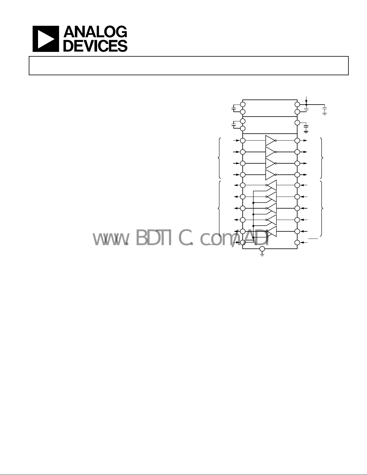
ADM560/ADM561
FUNCTIONAL BLOCK DIAGRAM
+3.3V INPUT
R1
R2
R3
R4
R5
1µF
10V
1µF
10V
12
C1+
14
C1–
15
C2+
16
C2–
7
6
20
21
8
5
26
22
19
24
+3.3V TO +6.6V
VOLTAGE
DOUBLER
+6.6V TO –6. 6V
VOLTAGE
INVERTER
T1
T2
T3
T4
R1
R2
R3
R4
R5
ADM560/
GND
ADM561
10
+
+
T1
IN
T2
IN
T3
IN
T4
IN
OUT
OUT
OUT
OUT
OUT
Figure 1.
11
V
CC
13
V+
17
V–
2
3
1
28
9
4
27
23
18
25
C3
+
1µF
6.3V
C4
+
1µF
10V
T1
T2
T3
T4
R1
R2
R3
R4
R5
SHDN (ADM560)
SHDN (ADM561)
OUT
OUT
OUT
OUT
IN
IN
IN
IN
IN
0.1µF
EIA/TI A-232
OUTPUTS
EIA/TI A-232
INPUTS
05667-001
GENERAL DESCRIPTION
The ADM560/ADM561 are four driver/five receiver interface
devices designed to meet the EIA-232 standard and operate with
a single +3.3 V power supply. The devices feature an on-board
dc-to-dc converter, eliminating the need for dual ±5 V power
supplies. This dc-to-dc converter contains a voltage doubler
and voltage inverter, both of which internally generate ±6.6 V
from the input +3.3 V power supply.
The ADM560 and the ADM561 consume only 5 mW making
em ideally suited for battery and other power-sensitive appli-
th
cations. A shutdown facility is also provided to reduce the power
to 0.66 μW.
The ADM560 contains active low shutdown and an active high
r
eceiver enable signal. In shutdown mode, two receivers remain
active, thereby allowing monitoring of peripheral devices. This
feature allows the device to be shut down until a peripheral
Rev. B
Information furnished by Analog Devices is believed to be accurate and reliable. However, no
responsibility is assumed by Anal og Devices for its use, nor for any infringements of patents or ot her
rights of third parties that may result from its use. Specifications subject to change without notice. No
license is granted by implication or otherwise under any patent or patent rights of Analog Devices.
Trademarks and registered trademarks are the property of their respective owners.
device begins communication. The active receivers alert the
p
rocessor, and then take the ADM560 out of shutdown mode.
The ADM561 features active high shutdown and an active
lo
w receiver enable. In this device, all receivers are disabled
in shutdown.
The ADM560/ADM561 are fabricated using CMOS technology
or minimal power consumption. They feature a high level of
f
over-voltage protection and latch-up immunity. The receiver
inputs can withstand up to ±25 V levels. The transmitter inputs
can be driven from either 3 V or 5 V logic levels. This allows
operation in mixed 3 V/5 V power supply systems.
The ADM560/ADM561 are packaged in a 28-lead SOIC and
a 28-lead SSO
P package.
One Technology Way, P.O. Box 9106, Norwood, MA 02062-9106, U.S.A.
Tel: 781.329.4700 www.analog.com
Fax: 781.461.3113 ©2006 Analog Devices, Inc. All rights reserved.

ADM560/ADM561
www.BDTIC.com/ADI
TABLE OF CONTENTS
Features.............................................................................................. 1
Pin Configuration and Function Descriptions..............................5
Applications....................................................................................... 1
Functional Block Diagram .............................................................. 1
General Description ......................................................................... 1
Revision History ............................................................................... 2
Specifications..................................................................................... 3
Absolute Maximum Ratings............................................................ 4
ESD Caution.................................................................................. 4
REVISION HISTORY
9/06—Rev. A to Rev. B
Updated Format..................................................................Universal
Changes to Specifications................................................................ 3
10/05—Rev. 0 to Rev. A
U
pdated Format..................................................................Universal
Changes to Specifications................................................................ 3
Update to Outline Dimensions....................................................... 9
Changes to Ordering Guide.......................................................... 10
Typical Performance Characteristics..............................................6
Theory of Operation .........................................................................8
Circuit Description .......................................................................8
Enable and Shutdown...................................................................8
Outline Dimensions..........................................................................9
Ordering Guide .......................................................................... 10
7/94—Revision 0: Initial Version
Rev. B | Page 2 of 12
ADM560/ADM561
www.BDTIC.com/ADI
SPECIFICATIONS
VCC = +3.3 V ± 10%, C1 to C4 = 1 μF, all specifications T
Table 1.
Parameter Min Typ Max Unit Test Conditions/Comments
Output Voltage Swing ±5.0 ±5.5 V VCC = 3.3 V, three transmitter outputs loaded with 3 kΩ to ground
±4 ±4.5 V VCC = 3.0 V, all transmitter outputs, loaded with 3 kΩ to ground
VCC Power Supply Current 3.5 5 mA No load, TIN = VCC
3.5 5 mA No load, TIN = GND
Shutdown Supply Current 0.2 5 μA
Input Logic Threshold Low, V
Input Logic Threshold High, V
Logic Pull-Up Current 3 20 μA TIN = GND
EIA-232 Input Voltage Range –25 +25 V
EIA-232 Input Threshold Low 0.4 0.8 V
EIA-232 Input Threshold High 1.1 2.4 V
EIA-232 Input Hysteresis 0.3 V
EIA-232 Input Resistance 3 5 7 kΩ
CMOS Output Voltage Low, VOL 0.4 V I
CMOS Output Voltage High, VOH 2.8 V I
CMOS Output Leakage Current +0.05 ±5 μA
Output Enable Time 100 ns
Output Disable Time 50 ns
Receiver Propagation Delay
TPHL 0.1 1 μs
TPLH 0.5 2 μs
Transition Region Slew Rate 4.5 V/μs
Transmitter Output Resistance 300 Ω VCC = V+ = V− = 0 V, V
RS-232 Output Short-Circuit Current ±10 mA
0.4 V
INL
2.4 V
INH
MIN
to T
, unless otherwise noted.
MAX
= GND (ADM560), SHDN = VCC (ADM561), TIN = VCC
SHDN
, EN, EN , SHDN, SHDN
T
IN
, EN, EN, SHDN, SHDN
T
IN
= 1.6 mA
OUT
= −40 mA
OUT
= VCC, EN = GND, 0 V ≤ R
EN
= 3 kΩ, CL = 2500 pF measured from +3 V to −3 V or
R
L
−3 V to +3 V
= ±2 V
OUT
OUT
≤ VCC
Rev. B | Page 3 of 12
ADM560/ADM561
www.BDTIC.com/ADI
ABSOLUTE MAXIMUM RATINGS
TA = 25°C, unless otherwise noted.
Table 2.
Parameter Rating
VCC −0.3 V to +6 V
V+ (VCC − 0.3 V) to +14 V
V− +0.3 V to −14 V
Input Voltages
TIN −0.3 V to (V+, +0.3 V)
RIN 25 V
Output Voltages
T
(V+, +0.3 V) to (V−, −0.3 V)
OUT
R
−0.3 V to (VCC + 0.3 V)
OUT
Short-Circuit Duration
T
Continuous
OUT
Power Dissipation
SSOP 900 mW
SOIC 900 mW
Operating Temperature Range
Commercial (J Version) 0°C to +70°C
Storage Temperature Range −65°C to +150°C
Lead Temperature
(Soldering, 10 sec)
ESD Rating >2000 V
+300°C
Stresses above those listed under Absolute Maximum Ratings
ma
y cause permanent damage to the device. This is a stress
rating only; functional operation of the device at these or any
other conditions above those indicated in the operational
section of this specification is not implied. Exposure to absolute
maximum rating conditions for extended periods may affect
device reliability.
ESD CAUTION
ESD (electrostatic discharge) sensitive device. Electrostatic charges as high as 4000 V readily accumulate on
the human body and test equipment and can discharge without detection. Although this product features
proprietary ESD protection circuitry, permanent damage may occur on devices subjected to high energy
electrostatic discharges. Therefore, proper ESD precautions are recommended to avoid performance
degradation or loss of functionality.
Rev. B | Page 4 of 12

ADM560/ADM561
www.BDTIC.com/ADI
PIN CONFIGURATION AND FUNCTION DESCRIPTIONS
T3
1
OUT
2
T1
OUT
T2
3
OUT
R2
4
IN
ADM560
5
R2
OUT
T2
IN
T1
IN
R1
OUT
R1
IN
GND
V
CC
C1+
V+
C1–
6
7
8
9
10
11
12
13
14
TOP VIEW
(Not to Scale)
T4
28
OUT
R3
27
IN
26
R3
OUT
SHDN
25
EN
24
23
R4
IN
R4
22
OUT
T4
21
IN
T3
20
IN
19
R5
OUT
R5
18
IN
V–
17
16
C2–
C2+
15
05667-002
Figure 2.ADM560 Pin Configuration Fig
Table 3. Pin Function Descriptions
Pin No. Mnemonic Description
2, 3, 1, 28 T1
9, 4, 27, 23, 18 R1IN to R5IN
OUT
to T4
Transmitter (Driver) Outputs. Typically ±6 V.
OUT
Receiver Inputs. These inputs accept RS-232 signal levels
connected on each of these inputs.
8, 5, 26, 22, 19 R1
7, 6, 20, 21 T1IN to T4IN
OUT
to R5
Receiver Outputs. These are 3 V logic levels.
OUT
Transmitter (Driver) Inputs. These inputs accept 3 V or 5
is connected on each input.
to V
CC
10 GND Ground Pin. Must be connected to 0 V.
11 VCC Power Supply Input 3.3 V ± 10%.
12, 14 C1+, C1− External Capacitor 1 is connected between these pins.
13 V+ Internally Generated Positive Supply. +6.6 V nominal.
15, 16 C2+, C2− External Capacitor 2 is connected between these pins.
17 V− Internally Generated Negative Supply. −6.6 V nominal.
24
25
Receiver Enable. EN, active high on ADM560. EN, active low on ADM561. Refer to Tabl e 4.
EN/EN
/SHDN Shutdown Control. SHDN, active low on ADM560. SHDN, active high on ADM561. Refer to Tabl e 4.
SHDN
T3
1
OUT
2
T1
OUT
T2
3
OUT
R2
4
IN
ADM561
5
R2
R1
OUT
T2
T1
OUT
R1
GND
V
C1+
C1–
IN
IN
IN
CC
V+
6
7
8
9
10
11
12
13
14
TOP VIEW
(Not to Scale)
ure 3. ADM561 Pin Configuration
. An internal 5 kΩ pull-down resistor to GND is
V logic levels. An internal 400 kΩ pull-up resistor
T4
28
OUT
R3
27
IN
26
R3
OUT
SHDN
25
EN
24
23
R4
IN
R4
22
OUT
T4
21
IN
T3
20
IN
19
R5
OUT
R5
18
IN
V–
17
16
C2–
C2+
15
05667-012
Table 4. ADM560/ADM561 Enable and Shutdown Control
ADM560 ADM561
Normal Operation
Shutdown Mode
SHDN = 1
EN = 1; receivers active
EN = 0; receivers inactive
SHDN = 0
EN = 1; Receiver R1 to Receiver R3 inactive
EN = 1; Receiver R4 and Receiver R5 active
SHDN = 0
= 0; receivers active
EN
EN = 1; receivers inactive
SHDN = 1
= 0; receivers inactive
EN
= 1; receivers inactive
EN
EN = 0; Receiver R1 to Receiver R5 inactive
Rev. B | Page 5 of 12

ADM560/ADM561
A
–
www.BDTIC.com/ADI
TYPICAL PERFORMANCE CHARACTERISTICS
6
5
4
160kbps
20kbps80kbps
0
TA = 25°C
= 3.3V
V
CC
4 TRANSMITT ERS LOADED
–1
–2
= 5kΩ || C
WITH R
L
C1 TO C4 = 1µF
L
(V)
3
OH
V
TA = 25°C
V
= 3.3V
CC
2
4 TRANSMITT ERS LOADE D
WITH R
= 5kΩ || C
L
C1 TO C4 = 1µF
1
0
500
0
Figure 4. Transmitter Output Volt
6.25
5.75
| (V)
OUT
| T
5.25
4.75
0
L
LOAD CAPACITANCE (pF)
age High vs. Load Capacitance
TA = 25°C
C1 TO C4 = 1µF
V
= 3.3V
CC
TRANSMITT ERS UNLOADED
T
HIGH
OUT
T
LOW
OUT
OUT
3421
| (mA)
| I
Figure 5. Transmitter Output Voltage vs. Load Current
(V)
–3
OL
V
–4
160kbps
–5
05667-005
3000
2500200015001000
–6
500
0
05667-006
5
Figure 7. Transmitter Output Voltage Low vs. Load Capacitance
45
40
35
30
25
TE (V/µs)
20
15
SLEW R
10
5
4 TRANSMITTERS
LOADED
0
500 2500200015001000
80kbps
20kbps
LOAD CAPACITANCE (pF)
3 TRANSMITT ERS
LOADED
LOAD CAPACITANCE (pF)
05667-008
2500200015001000
3000
05667-009
3000
Figure 8. Transmitter Slew Rate vs. Load Capacitance
10.5
9.5
8.5
7.5
(V)
OH
V
6.5
5.5
4.5
3.5
2.5
1 TRANSMIT TER
LOADED
TA = 25°C
C1 TO C4 = 1µF
TRANSMITT ERS LOADED
WITH 5kΩ || 2500pF
4 TRANSMITTERS
LOADED
(V)
V
CC
Figure 6. Transmitter Output Voltage High vs. V
5.04.54.03.53.0
05667-007
5.5
CC
Rev. B | Page 6 of 12
3
–4
–5
–6
(V)
OL
V
–10
–7
–8
–9
2.5
1 TRANSMIT TER
LOADED
3.0
VCC (V)
Figure 9. Transmitter Output Voltage Low vs. V
TA = 25°C
C1 TO C4 = 1µF
TRANSMITT ERS LOADED
WITH 5kΩ || 2500pF
4 TRANSMITT ERS
LOADED
5.04.54.03.5
CC
05667-010
5.5

ADM560/ADM561
www.BDTIC.com/ADI
10
TA = 25°C
V
= 3.3V
CC
C1 TO C4 = 1µF ALL TRANSMI TTERS UNL OADED
5
V+ AND V–
0
EQUALLY LOADED
V+ LOADED
NO LOAD ON V –
V– LOADED
NO LOAD ON V+
–5
OUTPUT VOLTAGE V+, V– (V)
–10
0
CURRENT (mA)
Figure 10. V+, V− vs. Load Current
201513105
05667-011
25
Rev. B | Page 7 of 12

ADM560/ADM561
www.BDTIC.com/ADI
THEORY OF OPERATION
The ADM560/ADM561 are RS-232 transmission line drivers/
receivers, and operate from a single +3.3 V supply. This is achieved
by integrating step-up voltage converters and level shifting transmitters and receivers onto the same chip. CMOS technology is
used to keep the power dissipation at an absolute minimum.
The ADM560/ADM561 are a modification, enhancement, and
improvement to the ADM241L family and its derivatives thereof.
These devices are essentially plug-in compatible and do not
have materially different applications.
Transmitter (Driver) Section
The drivers convert 3 V or 5 V logic input levels into EIA-232
output levels. With V
= +3.3 V and driving an EIA-232 load,
CC
the output voltage swing is typically ±5.5 V.
V
GND
CC
S1
S2
C1
S3
+
S4
+
C3
V+ = 2V
V
CC
CC
The ADM560/ADM561 contain an internal voltage doubler
nd a voltage inverter that generates ±6.6 V from the +3.3 V
a
input. Four external 1 μF capacitors are required for the internal voltage converters.
CIRCUIT DESCRIPTION
The internal circuitry consists of three main sections. These are
as follows:
charge pump voltage converter.
• A
• 3 V log
• EI
Charge Pump DC-to-DC Voltage Converter
The charge pump voltage converter consists of an oscillator and
a switching matrix. The converter generates a ±6.6 V supply from
the input +3.3 V level. This is done in two stages using a switched
capacitor technique (see Figure 11 and Figure 12). First, the
+3.3 V in
as the charge storage element. The +6.6 V level is then inverted
to generate −6.6 V using Capacitor C2 as the storage element.
Capacitor C3 and Capacitor C4 are used to reduce the output
ipple. Their values are not critical and can be reduced if higher
r
levels of ripple are acceptable. The C1 and C2 charge pump capacitors can also be reduced at the expense of the higher output
impedance on the V+ and V− supplies.
The V+ and V− supplies are also used to power external
cuitry if the current requirements are small.
cir
ic to EIA-232 transmitters.
A-232 to 3 V logic receivers.
put supply is doubled to +6.6 V using Capacitor C1
INTERNAL
OSCILLATOR
Figure 11. Charge Pump Voltage Double Operation
FROM
VO LTAGE
DOUBLER
V+
GND
INTERNAL
OSCILLATOR
S1
S2
Figure 12. Charge Pump Voltage Inverted Operation
C2
S3
+
S4
C4
GND
+
V– = – (V+)
Unused inputs can be left unconnected as an internal 400 kΩ
pull-up resistor pulls them high forcing the outputs into a low
state. The input pull-up resistors typically source 8 μA when
grounded, so connect unused inputs to V
or leave unconnec-
CC
ted in order to minimize power consumption.
Receiver Section
The receivers are inverting level shifters; they accept EIA-232
input levels and translate them into 3 V logic output levels. The
inputs have internal 5 kΩ pull-down resistors to ground and are
also protected against overvoltages of up to ±25 V. The guaranteed
switching thresholds are 0.4 V minimum and 2.4 V maximum.
Unconnected inputs are pulled to 0 V by the internal 5 kΩ pulldown resistor. This results in a Logic 1 output level for unconnected
inputs or for inputs connected to GND.
The receivers have a Schmitt trigger input with a hysteresis level
o
f 0.3 V. This ensures error-free reception for both noisy inputs
and for inputs with slow transition times.
ENABLE AND SHUTDOWN
Tabl e 4 shows the truth table for the enable and shutdown
control signals. When disabled all receivers are placed in a
high impedance state. In shutdown, all transmitters are disabled and all receivers on the ADM561 are disabled. On the
ADM560, Receiver R4 and Receiver R5 remain enabled in
shutdown.
05667-003
05667-004
Rev. B | Page 8 of 12

ADM560/ADM561
www.BDTIC.com/ADI
OUTLINE DIMENSIONS
10.50
10.20
9.90
2.00 MAX
0.05 MIN
COPLANARITY
0.10
0.30 (0.0118)
0.10 (0.0039)
COPLANARIT Y
0.10
0.38
0.22
15
5.60
5.30
8.20
5.00
7.80
1.85
1.75
1.65
SEATING
PLANE
7.40
14
28
1
0.65 BSC
COMPLIANT TO JEDEC STANDARDS MO-150-AH
Figure 13. 28-Lead Shrink Small Outline Package [SSOP]
S-28)
(R
Dimensions shown in millimeters
18.10 (0.7126)
17.70 (0.6969)
28
1
1.27 (0.0500)
BSC
0.51 (0.0201)
0.31 (0.0122)
15
7.60 (0.2992)
7.40 (0.2913)
14
10.65 (0.4193)
10.00 (0.3937)
2.65 (0.1043)
2.35 (0.0925)
SEATING
PLANE
8°
4°
0°
8°
0°
0.33 (0.0130)
0.20 (0.0079)
0.25
0.09
0
0
5
.
7
.
2
5
0.95
0.75
0.55
(
0
.
0
2
0
(
0
.
0
9
5
)
45°
9
8
)
1.27 (0.0500)
0.40 (0.0157)
060106-A
CONTROLL ING DIMENSIONS ARE IN MILLI METERS; INCH DIMENSIONS
(IN PARENTHESES) ARE ROUNDED-O FF MIL LIMET ER EQUIVALENTS FOR
REFERENCE ON LY AND ARE NOT APPROPRI ATE FOR USE IN DESIGN.
COMPLIANT TO JEDEC STANDARDS MS-013-AE
Figure 14. 28-Lead Standard Small Outline Package [SOIC_W]
Dimensions shown in millimeters and (inches)
Rev. B | Page 9 of 12
Wide Body
W-28)
(R
060706-A

ADM560/ADM561
www.BDTIC.com/ADI
ORDERING GUIDE
Model Temperature Range Package Description Package Option
ADM560JR 0°C to +70°C 28-Lead Standard Small Outline Package [SOIC_W] RW-28
ADM560JR-REEL 0°C to +70°C 28-Lead Standard Small Outline Package [SOIC_W] RW-28
ADM560JRZ
ADM560JRZ-REEL
ADM560JRS 0°C to +70°C 28-Lead Shrink Small Outline Package [SSOP] RS-28
ADM560JRS-REEL 0°C to +70°C 28-Lead Shrink Small Outline Package [SSOP] RS-28
ADM560JRSZ1 0°C to +70°C 28-Lead Shrink Small Outline Package [SSOP] RS-28
ADM560JRSZ-REEL
ADM561JR 0°C to +70°C 28-Lead Standard Small Outline Package [SOIC_W] RW-28
ADM561JR-REEL 0°C to +70°C 28-Lead Standard Small Outline Package [SOIC_W] RW-28
ADM561JRZ
ADM561JRZ-REEL
ADM561JRS 0°C to +70°C 28-Lead Shrink Small Outline Package [SSOP] RS-28
ADM561JRS-REEL 0°C to +70°C 28-Lead Shrink Small Outline Package [SSOP] RS-28
ADM561JRSZ
ADM561JRSZ-REEL
1
Z = Pb-free part.
1
1
1
0°C to +70°C 28-Lead Standard Small Outline Package [SOIC_W] RW-28
1
0°C to +70°C 28-Lead Standard Small Outline Package [SOIC_W] RW-28
1
0°C to +70°C 28-Lead Shrink Small Outline Package [SSOP] RS-28
0°C to +70°C 28-Lead Standard Small Outline Package [SOIC_W] RW-28
1
0°C to +70°C 28-Lead Standard Small Outline Package [SOIC_W] RW-28
0°C to +70°C 28-Lead Shrink Small Outline Package [SSOP] RS-28
1
0°C to +70°C 28-Lead Shrink Small Outline Package [SSOP] RS-28
Rev. B | Page 10 of 12

ADM560/ADM561
www.BDTIC.com/ADI
NOTES
Rev. B | Page 11 of 12

ADM560/ADM561
www.BDTIC.com/ADI
NOTES
©2006 Analog Devices, Inc. All rights reserved. Trademarks and
registered trademarks are the property of their respective owners.
D05667-0-9/06(B)
Rev. B | Page 12 of 12
 Loading...