Analog Devices ADM5180 Datasheet

a
Octal, RS-232/RS-423 Line Receiver
ADM5180
FEATURES
Eight Differential Line Receivers in One Package
Meets EIA Standard EIA-232E, 423A, 422A and
CCITT V.10, V.11, V.28
Single +5 V Supply
Differential Inputs Withstand ±25 V
Internal Hysteresis
Low Power CMOS –3.5 mA Supply Current
TTL/CMOS Compatible Outputs
Available in 28-Pin DIP and PLCC Packages
Low Power Replacement for UC5180C/NE5180
APPLICATIONS
High Speed Communication
Computer I-O Ports
Peripherals
High Speed Modems
Printers
Logic Level Translation
GENERAL DESCRIPTION
The ADM5180 is an octal differential line receiver suitable for a
wide range of digital communication systems with data rates up to
200 kB/s. Input signals conforming to EIA Standards 232-E, 422A
and CCITT V.10, V.11, V.28, X.26, and X.27 are accepted and
translated into TTL /CMOS output signal levels.
The ADM5180 is a superior upgrade for the UC5180C and the
NE5180. It is fabricated on an advanced BiCMOS process,
allowing high speed bipolar circuitry to be combined with low
power CMOS. This minimizes the power consumption to less than
25 mW.
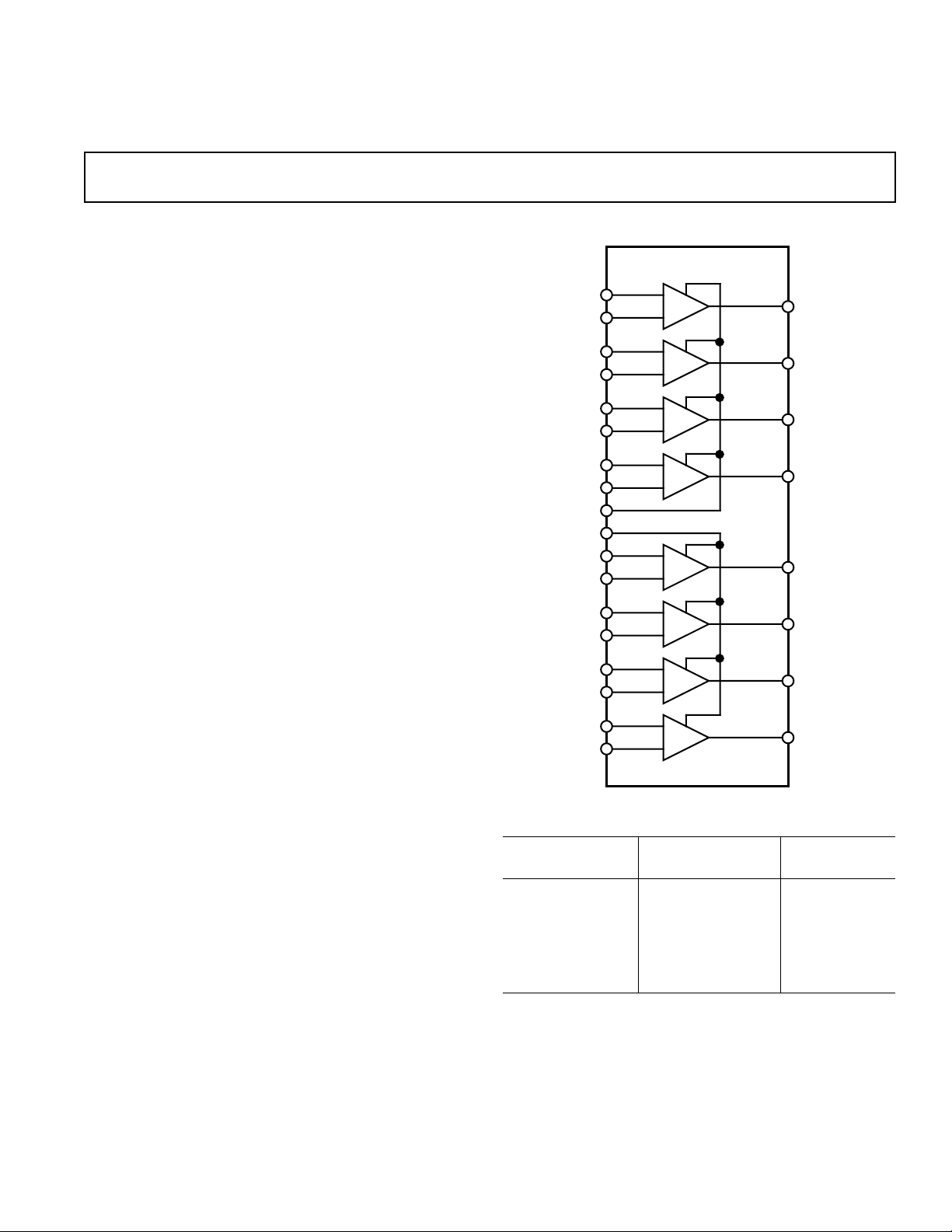
A failsafe function ensures a known output state under a variety of
input fault conditions as defined in RS-422A and RS-423A. The
failsafe function is controlled by FS1 and FS2. Each controls four
receivers. With FS = Low and a fault condition the output is forced
low while if FS = High, the output is forced high.
The device is available in both 28-pin DIP and 28-lead PLCC
packages.
FUNCTIONAL BLOCK DIAGRAM
ADM5180
A–
B–
C–
D–
FS1
FS2
E–
F–
G–
H–
A+
B+
C+
D+
E+
F+
G+
H+
A
B
C
D
E
F
G
H
A
O
B
O
C
O
D
O
E
O
F
O
G
O
H
O
Truth Table
Differential Input Failsafe Input Receiver
(+) - (–) FS1, FS2 Logic Output
>200 mV X H
<–200 mV X L
O/C L L
S/C L L
O/C H H
S/C H H
REV. 0
Information furnished by Analog Devices is believed to be accurate and
reliable. However, no responsibility is assumed by Analog Devices for its
use, nor for any infringements of patents or other rights of third parties
which may result from its use. No license is granted by implication or
otherwise under any patent or patent rights of Analog Devices.
One Technology Way, P.O. Box 9106, Norwood. MA 02062-9106, U.S.A.
Tel: 617/329-4700 Fax: 617/326-8703

(VDD = +5 V ± 5%, Input Common-Mode Range = ±7 V. All Specifications T
ADM5180–SPECIFICA TIONS
Parameter Min Typ Max Units Test Conditions/Comments
POWER REQUIREMENTS
V
DD
I
DD
INPUTS
Input Resistance, R
IN
Differential Input High Threshold, V
Differential Input Low Threshold, V
Hysteresis, V
Open Circuit Input Voltage, V
H
IOC
Input Capacitance 20 pF
Input Current, I
IN
OUTPUTS
High Level Output Voltage,V
Low Level Output Voltage ,V
Short Circuit O/P Current, I
OH
OL
OS
FAILSAFE FUNCTION
Failsafe Output Voltage, V
OFS
FS1, FS2 Input Current –10 +10 µA
4.75 5.25 V
37kΩ3 V ≤|VIN|≤ 25 V
50 200 mV RS = 0 Ω, V
TH
–200 –50 mV RS = 0 Ω, V
TL
–400 mV R
50 140 mV FS1, FS2 = 0 V or VDD, See Figure 1
–3.25 mA VIN = –10 V
2.7 V VID = 1.0 V, I
2.7 V 0 ≥ I
T
unless otherwise noted.)
MAX
3.5 5 mA
400 mV R
60 mV
3.25 mA VIN = +10 V
0.4 V VID = –1.0 V, I
0.45 V V
100 mA Note 1
0.40 V 0 ≤ I
0.45 V 0 ≤ I
= 500 Ω, V
S
= 500 Ω, V
S
= –1.0 V, I
ID
= 2.7 V, I
OUT
= 2.7 V, I
OUT
= 0.45 V, I
OUT
= 0.45 V, I
OUT
= –440 µA
OUT
= 4 mA
OUT
= 8 mA, TA = 0ºC to +70ºC
OUT
= –440 µA, See Figure 1
OUT
OUT
= 8 mA, See Figure 1
OUT
OUT
Inputs Open or Shorted Together or One Input Open
and One Grounded
≤ 4 mA; FS1, FS2 = 0 V
OUT
≤ 8 mA, TA = 0ºC to +70ºC; FS1, FS2 = 0 V
OUT
≥ –400 µA; FS1, FS2 = V
OUT
to
MIN
= –440 µA, See Figure 1
= 8 mA, See Figure 1
DD
NOTE
1
Only one output may be shorted at any time.
Specifications subject to change without notice.
TIMING CHARACTERISTICS
(VDD = +5 V ± 5%. All Specifications T
MIN
to T
unless otherwise noted)
MAX
Parameter Min Typ Max Units Test Conditions/Comments
Propagation Delay–Low to High 550 ns CL = 50 pF, VIN = ±500 mV
Propagation Delay–High to Low 550 ns CL = 50 pF, VIN = ±500 mV
Acceptable Input Frequency 0.1 MHz Unused Input Grounded, V
= ±200 mV
IN
Rejectable Input Frequency 5.5 MHz Unused Input Grounded, VIN = ±500 mW
Specifications subject to change without notice.
–2–
REV. 0
 Loading...