

5 V Low Power
www.BDTIC.com/ADI
FEATURES
Meets EIA RS-485 standard
5 Mbps data rate
Single 5 V supply
–7 V to +12 V bus common-mode range
High speed, low power BiCMOS
Thermal shutdown protection
Short-circuit protection
Driver propagation delay: 10 ns typical
Receiver propagation delay: 15 ns typical
High-Z outputs with power off
Superior upgrade for LTC485
APPLICATIONS
Low power RS-485 systems
DTE/DCE interface
Packet switching
Local area networks (LNAs)
Data concentration
Data multiplexers
Integrated services digital network (ISDN)
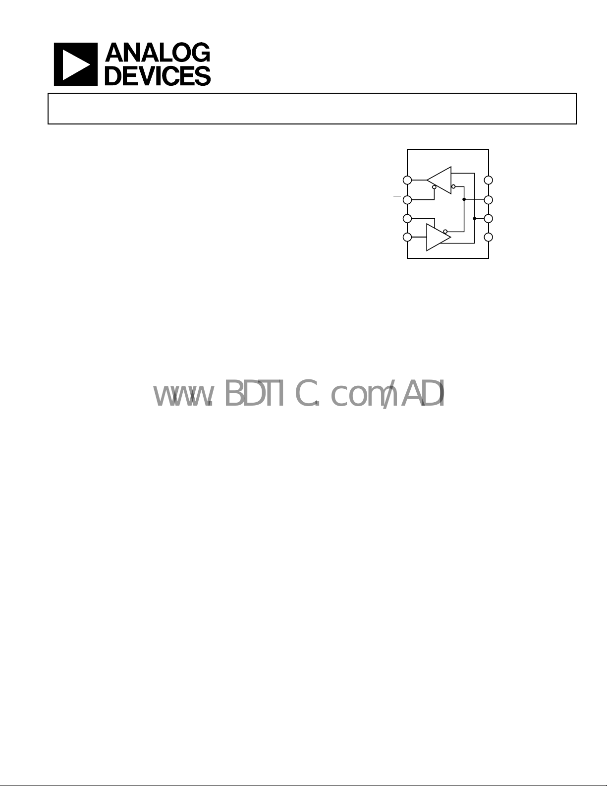
EIA RS-485 Transceiver
ADM485
FUNCTIONAL BLOCK DIAGRAM
ADM485
RO
RE
DE
1
2
3
4
DI
R
D
Figure 1.
8
V
CC
7
B
6
A
5
GND
00078-001
GENERAL DESCRIPTION
The ADM485 is a differential line transceiver suitable for high
speed bidirectional data communication on multipoint bus
transmission lines. It is designed for balanced data transmission
and complies with EIA standards RS-485 and RS-422. The part
contains a differential line driver and a differential line receiver.
Both the driver and the receiver can be enabled independently.
When disabled, the outputs are three-stated.
The ADM485 operates from a single 5 V power supply.
xcessive power dissipation caused by bus contention or by
E
output shorting is prevented by a thermal shutdown circuit. If
during fault conditions, a significant temperature increase is
detected in the internal driver circuitry, this feature forces the
driver output into a high impedance state.
Up to 32 transceivers can be connected simultaneously on a
bu
s, but only one driver should be enabled at any time. It is
important, therefore, that the remaining disabled drivers do not
load the bus. To ensure this, the ADM485 driver features high
output impedance when disabled and when powered down,
which minimizes the loading effect when the transceiver is not
being used. The high impedance driver output is maintained
over the common-mode voltage range of −7 V to +12 V.
Rev. F
Information furnished by Analog Devices is believed to be accurate and reliable. However, no
responsibility is assumed by Anal og Devices for its use, nor for any infringements of patents or ot her
rights of third parties that may result from its use. Specifications subject to change without notice. No
license is granted by implication or otherwise under any patent or patent rights of Analog Devices.
Trademarks and registered trademarks are the property of their respective owners.
The receiver contains a fail-safe feature that results in a logic
high output state if the inputs are unconnected (floating).
The ADM485 is fabricated on BiCMOS, an advanced mixed
t
echnology process combining low power CMOS with fast
switching bipolar technology. All inputs and outputs contain
protection against ESD; all driver outputs feature high source
and sink current capability. An epitaxial layer is used to guard
against latch-up.
The ADM485 features extremely fast switching speeds. Minimal
dr
iver propagation delays permit transmission at data rates up
to 5 Mbps while low skew minimizes EMI interference.
The part is fully specified over the commercial and industrial
t
emperature range and is available in 8-lead PDIP, 8-lead SOIC,
and small footprint, 8-lead MSOP packages.
One Technology Way, P.O. Box 9106, Norwood, MA 02062-9106, U.S.A.
Tel: 781.329.4700 www.analog.com
Fax: 781.461.3113 ©1993–2008 Analog Devices, Inc. All rights reserved.

ADM485
www.BDTIC.com/ADI
TABLE OF CONTENTS
Features .............................................................................................. 1
Applications....................................................................................... 1
Functional Block Diagram .............................................................. 1
General Description......................................................................... 1
Revision History ............................................................................... 2
Specifications..................................................................................... 3
Timing Specifications .................................................................. 4
Absolute Maximum Ratings............................................................ 5
ESD Caution.................................................................................. 5
Pin Configuration and Function Descriptions............................. 6
Typical Performance Characteristics ............................................. 7
REVISION HISTORY
04/08—Rev. E to Rev. F
Updated Format..................................................................Universal
hanges to Table 2............................................................................ 4
C
Updated Outline Dimension......................................................... 13
Changes to Ordering Guide.......................................................... 14
10/03—Rev. D to Rev. E
Changes to Timing Specifications.................................................. 2
Updated Ordering Guide................................................................. 3
7/03—Rev. C to Rev. D
Changes to Absolute Maximum Ratings....................................... 3
Changes to Ordering Guide............................................................ 3
Update to Outline Dimensions....................................................... 9
Test Cir c ui t s ..................................................................................... 10
Switching Characteristics .............................................................. 11
Applications Information.............................................................. 12
Differential Data Transmission ................................................ 12
Cable and Data Rate................................................................... 12
Thermal Shutdown .................................................................... 12
Propagation Delay ...................................................................... 12
Receiver Open Circuit, Fail-Safe.............................................. 12
Outline Dimensions ....................................................................... 13
Ordering Guide .......................................................................... 14
1/03—Rev. B to Rev. C.
Change to Specifications ..................................................................2
Change to Ordering Guide...............................................................3
12/02—Rev. A to Rev. B.
Deleted Q-8 Package..........................................................Universal
Edits to Features.................................................................................1
Edits to General Description ...........................................................1
Edits, additions to Specifications.....................................................2
Edits, additions to Absolute Maximum Ratings............................3
Additions to Ordering Guide...........................................................3
TPCs Updated and Reformatted .....................................................5
Addition of 8-Lead MSOP Package ................................................9
Update to Outline Dimensions........................................................9
Rev. F | Page 2 of 16
ADM485
www.BDTIC.com/ADI
SPECIFICATIONS
VCC = 5 V ± 5%, all specifications T
Table 1.
Parameter Min Typ Max Unit Test Conditions/Comments
DRIVER
Differential Output Voltage, VOD 5.0 V R = ∞, see Figure 20
2.0 5.0 V VCC = 5 V, R = 50 Ω (RS-422), see Figure 20
1.5 5.0 V R = 27 Ω (RS-485), see Figure 20
V
1.5 5.0 V V
OD3
Δ|VOD| for Complementary Output States 0.2 V R = 27 Ω or 50 Ω, see Figure 20
Common-Mode Output Voltage, VOC 3 V R = 27 Ω or 50 Ω, see Figure 20
Δ|VOD| for Complementary Output States 0.2 V R = 27 Ω or 50 Ω
Output Short-Circuit Current, V
Output Short-Circuit Current, V
CMOS Input Logic Threshold Low, V
CMOS Input Logic Threshold High, V
Logic Input Current (DE, DI) ±1.0 μA
RECEIVER
Differential Input Threshold Voltage, VTH −0.2 +0.2 V −7 V ≤ VCM ≤ +12 V
Input Voltage Hysteresis, ΔVTH 70 mV VCM = 0 V
Input Resistance 12 kΩ −7 V ≤ VCM ≤ +12 V
Input Current (A, B) 1 mA VIN = 12 V
–0.8 mA VIN = −7 V
CMOS Input Logic Threshold Low, V
CMOS Input Logic Threshold High, V
Logic Enable Input Current (RE)
CMOS Output Voltage Low, VOL 0.4 V I
CMOS Output Voltage High, VOH 4.0 V I
Short-Circuit Output Current 7 85 mA V
Three-State Output Leakage Current ±1.0 μA 0.4 V ≤ V
POWER SUPPLY CURRENT
ICC, Outputs Enabled
ICC, Outputs Disabled
to T
MIN
= High 35 250 mA −7 V ≤ VO ≤ +12 V
OUT
= Low 35 250 mA −7 V ≤ VO ≤ +12 V
OUT
INL
INH
INL
INH
, unless otherwise noted.
MAX
0.8 V
2.0 V
0.8 V
2.0 V
±1
μA
= −7 V to +12 V, see Figure 21
TST
= 4.0 mA
OUT
= −4.0 mA
OUT
= GND or VCC
OUT
OUT
1.0 2.2 mA Digital inputs = GND or V
0.6 1 mA Digital inputs = GND or V
≤ 2.4 V
CC
CC
Rev. F | Page 3 of 16
ADM485
www.BDTIC.com/ADI
TIMING SPECIFICATIONS
VCC = 5 V ± 5%, all specifications T
Table 2.
Parameter Min Typ Max Unit Test Conditions/Comments
DRIVER
Propagation Delay Input to Output, t
Driver Output to OUTPUT, t
SKEW
Driver Rise/Fall Time, tR, tF 8 15 ns R
Driver Enable to Output Valid 10 25 ns RL = 110 Ω, CL = 50 pF, see Figure 23
Driver Disable Timing 10 25 ns RL = 110 Ω, CL = 50 pF, see Figure 23
Matched Enable Switching |tZH − tZL| 0 2 ns RL = 110 Ω, CL = 50 pF, see Figure 231
Matched Disable Switching |tHZ − tLZ| 0 2 ns RL = 110 Ω, CL = 50 pF, see Figure 231
RECEIVER
Propagation Delay Input to Output, t
Skew |t
Receiver Enable, tZH, t
PLH
− t
| 5 ns CL = 15 pF, see Figure 24
PHL
ZL
Receiver Disable, tHZ, tLZ 5 20 ns CL = 15 pF, RL = 1 kΩ, see Figure 25
Tx Pulse Width Distortion 1 ns
Rx Pulse Width Distortion 1 ns
1
Guaranteed by characterization.
to T
MIN
, unless otherwise noted.
MAX
, t
2 10 15 ns R
PLH
PHL
1 5 ns
, t
8 15 30 ns CL = 15 pF, see Figure 24
PLH
PHL
= 54 Ω, CL1 = CL2 = 100 pF, see Figure 22
LDIFF
= 54 Ω, CL1 = CL2 = 100 pF, see Figure 22
R
LDIFF
= 54 Ω, CL1 = CL2 = 100 pF, see Figure 22
LDIFF
5 20 ns CL = 15 pF, RL = 1 kΩ, see Figure 25
Rev. F | Page 4 of 16
ADM485
www.BDTIC.com/ADI
ABSOLUTE MAXIMUM RATINGS
TA = 25°C, unless otherwise noted.
Table 3.
Parameter Rating
V
CC
Inputs
Driver Input (DI) −0.3 V to VCC + 0.3 V
Control Inputs (DE, RE)
Receiver Inputs (A, B) −9 V to +14 V
Outputs
Driver Outputs (A, B) −9 V to +14 V
Receiver Output −0.5 V to VCC + 0.5 V
Power Dissipation 8-Lead MSOP 900 mW
θJA, Thermal Impedance 206°C/W
Power Dissipation 8-Lead PDIP 500 mW
θJA, Thermal Impedance 130°C/W
Power Dissipation 8-Lead SOIC 450 mW
θJA, Thermal Impedance 170°C/W
Operating Temperature Range
Commercial Range (J Version) 0°C to 70°C
Industrial Range (A Version) −40°C to +85°C
Storage Temperature Range −65°C to +150°C
Lead Temperature (Soldering, 10 sec) 300°C
Vapor Phase (60 sec) 215°C
Infrared (15 sec) 220°C
−0.3 V to +7 V
−0.3 V to V
CC
+ 0.3 V
Stresses above those listed under Absolute Maximum Ratings
may cause permanent damage to the device. This is a stress
rating only; functional operation of the device at these or any
other conditions above those indicated in the operational
section of this specification is not implied. Exposure to absolute
maximum rating conditions for extended periods may affect
device reliability.
Table 4. Transmitting
Inputs Outputs
DE DI B A
1 1 0 1
1 0 1 0
0 X
1
X = don’t care.
2
Z = high impedance.
1
Z2 Z2
Table 5. Receiving
RE
0 ≥ +0.2 V 1
0 ≤ −0.2 V 0
0 Inputs open 1
1
1
X = don’t care.
2
Z = high impedance.
Input A − Input B Output RO
1
X
Z2
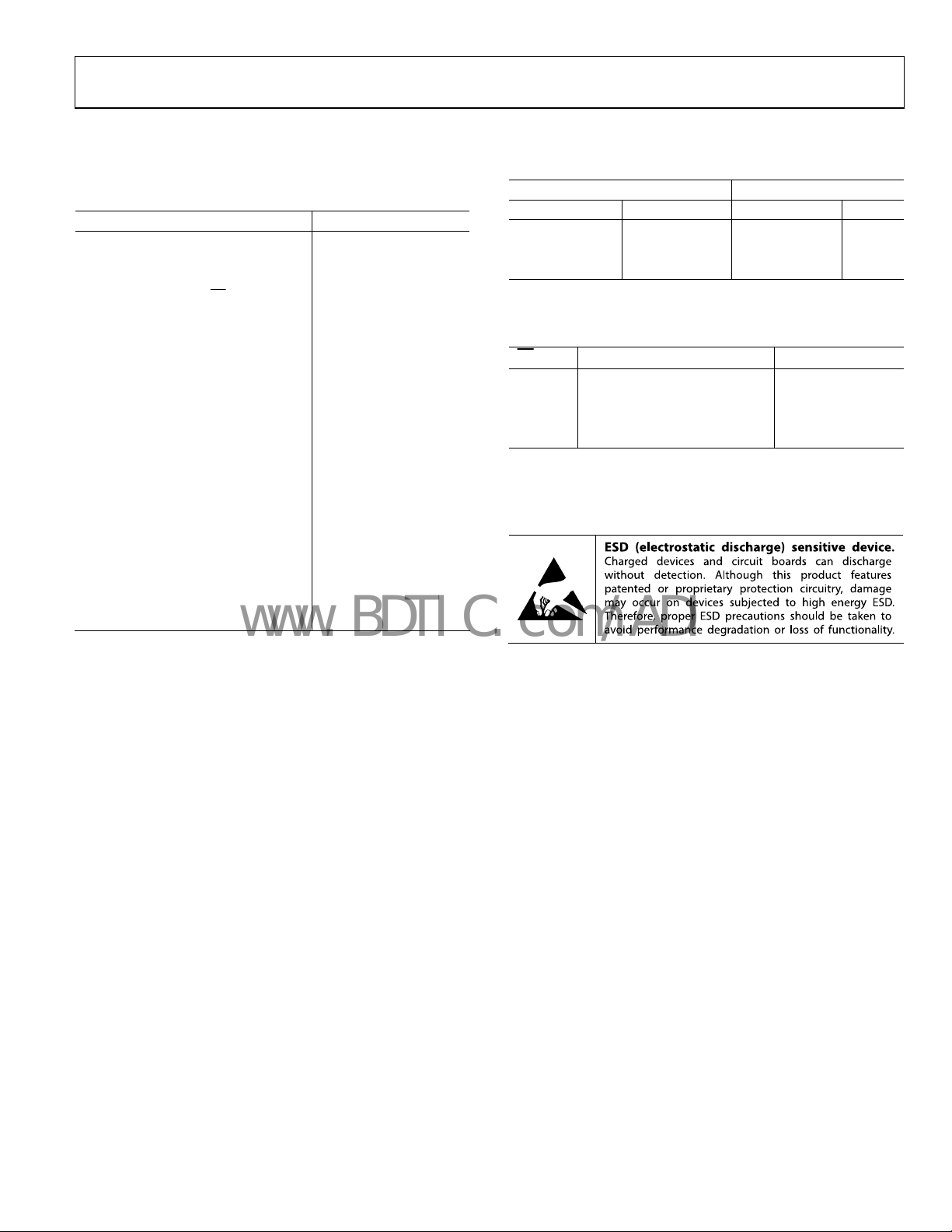
ESD CAUTION
Rev. F | Page 5 of 16

ADM485
www.BDTIC.com/ADI
PIN CONFIGURATION AND FUNCTION DESCRIPTIONS
1
RO
2
RE
ADM485
TOP VIEW
DE
3
(Not to Scale)
DI
4
Figure 2. Pin Configuration
8
V
CC
7
B
A
6
GND
5
00078-002
Table 6. Pin Function Descriptions
Pin No. Mnemonic Function
1 RO Receiver Output. When enabled, if A is greater than B by 200 mV, RO is high. If A is less than B by 200 mV, RO is low.
2
3 DE
RE
Receiver Output Enable. A low level enables the receiver output, RO. A high level places it in a high impedance state.
Driver Output Enable. A high level enables the driver differen
tial outputs, A and B. A low level places it in a high
impedance state.
4 DI
Driver Input. When the driver is enabled, a logic low on DI forces A low and B high, while a logic high on DI forces
A high and B low
.
5 GND Ground Connection, 0 V.
6 A Noninverting Receiver Input A/Driver Output A.
7 B Inverting Receiver Input B/Driver Output B.
8 VCC Power Supply, 5 V ± 5%.
Rev. F | Page 6 of 16

ADM485
www.BDTIC.com/ADI
TYPICAL PERFORMANCE CHARACTERISTICS
50
45
40
35
30
25
20
15
OUTPUT CURRENT (mA)
10
5
0
0.25 0.50 0.75 1.00 1.25 1.50 1.75 2. 00
0
Figure 3. Output Current vs. R
RECEIVER OUTPUT LOW VOLTAGE (V)
eceiver Output Low Voltage
0
–2
–4
–6
–8
–10
–12
OUTPUT CURRENT (mA)
–14
–16
–18
3.50 3.75 4.00 4.25 4.50 4.75 5.00
RECEIVER OUTPUT HIGH VOL TAGE (V)
Figure 4. Output Current vs. Receiver Output High Voltage
4.55
4.50
4.45
I = 8mA
00078-003
00078-004
0.40
0.35
0.30
0.25
0.20
RECEIVER OUT PUT LOW VOLT AGE (V)
0.15
–25 0 25 50 75 100 125
–50
TEMPERATURE (° C)
Figure 6. Receiver Output Low Voltage vs. Temperature
90
80
70
60
50
40
30
OUTPUT CURRENT (mA)
20
10
0
0 0. 5 1. 0 1.5 2.0 2.5 3.0 3.5 4.0 4.5
DRIVER DIFF ERENTIAL O UTPUT VO LTAGE (V)
Figure 7. Output Current vs. Driver D
ifferential Output Voltage
2.15
RL = 26.8Ω
2.10
I = 8mA
0078-006
0078-007
4.40
4.35
4.30
4.25
4.20
RECEIVER OUT PUT HIG H VOLTAG E (V)
4.15
–50 –25 0 25 50 75 100 125
TEMPERATURE (°C)
0078-005
Figure 5. Receiver Output High Voltage vs. Temperature
Rev. F | Page 7 of 16
2.05
2.00
1.95
DRIVER DIFF ERENTIAL OUTPUT VO LTAGE (V)
1.90
–50 –25 0 25 50 75 100 125
TEMPERATURE (° C)
Figure 8. Driver Differential Output Voltage vs. Temperature
00078-008

ADM485
www.BDTIC.com/ADI
100
90
80
70
60
50
40
30
OUTPUT CURRENT (mA)
20
10
0
04
DRIVER OUTPUT LOW VOLTAGE (V)
Figure 9. Output Current vs. Driv
0 3.52.0 2.51.00.5 1.5 .5
.043.
00078-009
er Output Low Voltage
0
–10
–20
–30
–40
–50
–60
–70
–80
OUTPUT CURRENT – mA
–90
–100
–110
–120
0 0.5 1.0 1.5 2.0 2. 5 3.0 3.5 4. 0 4.5 5.0
Figure 10. Output Current vs. Driv
DRIVER OUTPUT HIGH VO LTAGE ( V)
er Output High Voltage
00078-010
1.1
0.7
0.6
0.5
|
t
–
t
|
PLH
0.4
0.3
RECEIVER SKEW (ns)
0.2
0.1
0
–50 –25 0 25 50 75 100 125
TEMPERATURE (°C)
PHL
Figure 12. Receiver Skew vs. Temperature
6
5
4
3
| t
– t
PHLA
2
DRIVER SKEW ( ns)
1
0
–50 –25 0 2 5 50 75 100 125
| t
PLHA
|
PHLB
– t
|
PLHB
TEMPERATURE ( °C)
Figure 13. Driver Skew vs. Temperature
1.4
00078-012
00078-013
1.0
DRIVER ENABLED
0.9
0.8
0.7
SUPPLY CURRENT (mA)
0.6
0.5
–50 –25 0 25 50 75 100 125
DRIVER DISABLE D
TEMPERATURE (° C)
00078-011
Figure 11. Supply Current vs. Temperature
Rev. F | Page 8 of 16
1.2
1.0
0.8
PWD
0.6
0.4
0.2
0
–50 –25 0 25 50 75 100 125 150
TEMPERATURE ( °C)
|
t
–
t
|
PLH
PHL
Figure 14. Driver Pulse Width Distortion (PWD) vs. Temperature
00078-014

ADM485
www.BDTIC.com/ADI
T
T
1,2
CH1 1.00VΩ
B
W
CH2 1.00VΩ
B
W
Figure 15. Unloaded Driver Differential Outputs
M5.00ns CH3 2.64V
A
B
00078-015
4
1,2
3
CH1 1.00VΩ
CH3 5.00VΩ
B
W
B
W
CH2 1.00VΩ
CH4 2.00VΩ
B
M10.00ns CH4 2.76V
W
B
W
DI
A
B
RO
00078-018
Figure 18. Driver/Receiver Propagation Delays, High to Low
A
B
A
B
1,2
CH1 1.00VΩ
B
W
CH2 500mVΩ
B
M5.00ns CH3 2.74V
W
Figure 16. Loaded Driver Differential Outputs
T
4
1,2
3
CH1 1.00VΩ
CH3 5.00VΩ
B
W
B
W
CH2 1.00VΩ
CH4 2.00VΩ
B
M10.0ns CH4 400mV
W
B
W
Figure 17. Driver/Receiver Propagation Delays, Low to High
1,2
00078-016
CH1 500mVΩ CH2 500mVΩ M10.00ns CH4 2. 76V
0078-019
Figure 19. Driver Output at 30 Mbps
DI
A
B
RO
00078-017
Rev. F | Page 9 of 16

ADM485
Ω
V
A
V
+
V
–
V
www.BDTIC.com/ADI
TEST CIRCUITS
R
V
OD
V
R
OC
Figure 20. Driver Voltage Measurement
375
60Ω
V
OD3
375Ω
V
TST
Figure 21. Driver Voltage Measurement
A
R
LDIFF
B
C
L1
C
L2
Figure 22. Driver Propagation Delay
A
0V OR 3V
0078-020
DE IN
DE
C
V
OUT
B
L
Figure 23. Driver Enable/Disable
V
RE
B
00078-021
C
L
OUT
Figure 24. Receiver Propagation Delay
1.5
S1
1.5
RE
00078-022
IN
RE
CLV
OUT
R
L
Figure 25. Receiver Enable/Disable
CC
R
L
S2S1
00078-023
00078-024
CC
S2
00078-025
Rev. F | Page 10 of 16

ADM485
V
–V
A
A
V
V
www.BDTIC.com/ADI
SWITCHING CHARACTERISTICS
3
0V
B
V
A
+V
0V
O
1.5V
t
PLH
1/2V
O
O
t
=
t
PLH
–
O
10% POINT
90% POINT
SKEW
t
R
Figure 26. Driver Propagation Delay, Rise/Fall Timing
DE
1.5V
t
ZL
t
PHL
1.5V
t
1.5V
LZ
t
PHL
90% POINT
10% POINT
t
F
3
0V
A, B
RO
00078-026
0V
t
PLH
1.5V
t
=
t
SKEW
PLH
0V
t
PHL
V
OH
–
t
PHL
1.5V
V
OL
Figure 28. Receiver Propagation Delay
3
RE
1.5V
t
ZL
1.5V
t
LZ
0V
00078-028
, B
, B
2.3V
t
ZH
2.3V
V
OL
t
HZ
V
OH
Figure 27. Driver Enable/Disable Timing
+ 0.5V
– 0.5V
RO
V
OL
V
OH
0V
00078-027
RO
0V
1.5V
OUTPUT LOW
t
ZH
OUTPUT HIGH
1.5V
t
HZ
VOL + 0.5V
V
OH
Figure 29. Receiver Enable/Disable Timing
– 0.5V
V
OL
V
OH
00078-029
Rev. F | Page 11 of 16

ADM485
www.BDTIC.com/ADI
APPLICATIONS INFORMATION
DIFFERENTIAL DATA TRANSMISSION
Differential data transmission is used to reliably transmit data at
high rates over long distances and through noisy environments.
Differential transmission nullifies the effects of ground shifts
and noise signals that appear as common-mode voltages on the
line. There are two main standards approved by the EIA that
specify the electrical characteristics of transceivers used in
differential data transmission.
The RS-422 standard specifies data rates up to 10 MBaud and
line len
gths up to 4000 ft. A single driver can drive a transmission
line with up to 10 receivers.
To cater to true multipoint communications, the RS-485
andard was defined. This standard meets or exceeds all the
st
requirements of RS-422 but also allows for up to 32 drivers and
32 receivers to be connected to a single bus. An extended commonmode range of −7 V to +12 V is defined. The most significant
difference between the RS-422 standard and the RS-485 standard is
the fact that the drivers can be disabled, thereby allowing more
than one (32 in fact) to be connected to a single line. Only one
driver should be enabled at a time, but the RS-485 standard
contains additional specifications to guarantee device safety in
the event of line contention.
Table 7. Comparison of RS-422 and RS-485 Interface Standards
Specification RS-422 RS-485
Transmission Type Differential Differential
Maximum Cable Length 4000 ft. 4000 ft.
Minimum Driver Output Voltage ±2 V ±1.5 V
Driver Load Impedance 100 Ω 54 Ω
Receiver Input Resistance 4 kΩ min 12 kΩ min
Receiver Input Sensitivity ±200 mV ±200 mV
Receiver Input Voltage Range −7 V to +7 V −7 V to +12 V
No. of Drivers/Receivers per Line 1/10 32/32
CABLE AND DATA RATE
The transmission line of choice for RS-485 communications is
a twisted pair. Twisted pair cable tends to cancel common-mode
noise and causes cancellation of the magnetic fields generated
by the current flowing through each wire, thereby reducing the
effective inductance of the pair.
The ADM485 is designed for bidirectional data communications
n multipoint transmission lines. A typical application showing
o
a multipoint transmission network is illustrated in
An RS-48
on the bus. Only one driver can transmit at a particular time,
but multiple receivers can be enabled simultaneously.
5 transmission line can have as many as 32 transceivers
Figure 30.
RT
D
R
R
DD
Figure 30. Typical RS-485 Network
As with any transmission line, it is important that reflections be
minimized. This can be achieved by terminating the extreme ends
of the line using resistors equal to the characteristic impedance of
the line. Stub lengths of the main line should also be kept as
short as possible. A properly terminated transmission line appears
purely resistive to the driver.
RT
D
R
R
THERMAL SHUTDOWN
The ADM485 contains thermal shutdown circuitry that protects
the part from excessive power dissipation during fault conditions.
Shorting the driver outputs to a low impedance source can result
in high driver currents. The thermal sensing circuitry detects
the increase in die temperature and disables the driver outputs.
The thermal sensing circuitry is designed to disable the driver
outputs when a die temperature of 150°C is reached. As the
device cools, the drivers are re-enabled at 140°C.
PROPAGATION DELAY
The ADM485 features very low propagation delay, ensuring
maximum baud rate operation. The driver is well balanced,
ensuring distortion free transmission.
Another important specification is a measure of the skew
een the complementary outputs. Excessive skew impairs
betw
the noise immunity of the system and increases the amount of
electromagnetic interference (EMI).
RECEIVER OPEN CIRCUIT, FAIL-SAFE
The receiver input includes a fail-safe feature that guarantees a
logic high on the receiver when the inputs are open circuit or
floating.
0078-030
Rev. F | Page 12 of 16

ADM485
www.BDTIC.com/ADI
OUTLINE DIMENSIONS
5.00 (0.1968)
4.80 (0.1890)
4.00 (0.1574)
3.80 (0.1497)
0.25 (0.0098)
0.10 (0.0040)
COPLANARITY
0.10
CONTROLL ING DIMENSI ONS ARE IN MILLIMETERS; INCH DI MENSIONS
(IN PARENTHESES) ARE ROUNDED-OFF MILLIMETER EQUIVALENTS FOR
REFERENCE ONLY AND ARE NOT APPROPRI ATE FOR USE IN DES IGN.
85
1
1.27 (0.0500)
SEATING
PLANE
COMPLIANT TO JEDEC STANDARDS MS-012-A A
BSC
6.20 (0.2441)
5.80 (0.2284)
4
1.75 (0.0688)
1.35 (0.0532)
0.51 (0.0201)
0.31 (0.0122)
8°
0°
0.25 (0.0098)
0.17 (0.0067)
0.50 (0.0196)
0.25 (0.0099)
1.27 (0.0500)
0.40 (0.0157)
45°
012407-A
Figure 31. 8-Lead Standard Small Outline Package [SOIC_N]
Narrow B
ody (R-8)
Dimensions shown in millimeters and (inches)
3.20
3.00
2.80
8
5
4
SEATING
PLANE
5.15
4.90
4.65
1.10 MAX
0.23
0.08
8°
0°
0.80
0.60
0.40
3.20
3.00
2.80
PIN 1
0.95
0.85
0.75
0.15
0.00
COPLANARITY
1
0.65 BSC
0.38
0.22
0.10
COMPLIANT TO JEDEC STANDARDS MO-187-AA
Figure 32. 8-Lead Mini Small Outline Package [MSOP]
Dim
ensions shown in millimeters
Rev. F | Page 13 of 16
(RM-8)

ADM485
www.BDTIC.com/ADI
0.400 (10.16)
0.365 (9.27)
0.355 (9.02)
0.210 (5.33)
0.150 (3.81)
0.130 (3.30)
0.115 (2.92)
0.022 (0.56)
0.018 (0.46)
0.014 (0.36)
MAX
8
1
0.100 (2.54)
0.070 (1.78)
0.060 (1.52)
0.045 (1.14)
BSC
5
4
0.280 (7. 11)
0.250 (6.35)
0.240 (6.10)
0.015
(0.38)
MIN
SEATING
PLANE
0.005 (0.13)
MIN
0.060 (1.52)
MAX
0.015 (0.38)
GAUGE
PLANE
0.325 (8.26)
0.310 (7.87)
0.300 (7.62)
0.430 (10.92)
MAX
0.195 (4.95)
0.130 (3.30)
0.115 (2.92)
0.014 (0.36)
0.010 (0.25)
0.008 (0.20)
CONTROLLING DIMENSIONSARE IN INCHES; MILLIMETER DIMENSIONS
(IN PARENTHESES) ARE ROUNDED-OFF INCH EQUIVALENTS FOR
REFERENCE ON LY AND ARE NOT APPRO PRIATE FOR USE IN DESIGN.
CORNER LEADS MAY BE CONFIGURED AS WHOLE OR HALF LEADS.
COMPLIANT TO JEDEC STANDARDS MS-001
070606-A
Figure 33. 8-Lead Plastic Dual In-Line Package [PDIP]
Narrow B
ody (N-8)
Dimensions shown in inches and (millimeters)
ORDERING GUIDE
Model Temperature Range Package Description Package Option Branding
ADM485AN −40°C to +85°C 8-Lead PDIP N-8
ADM485ANZ
ADM485AR −40°C to +85°C 8-Lead SOIC_N R-8
ADM485AR-REEL −40°C to +85°C 8-Lead SOIC_N R-8
ADM485ARZ
ADM485ARZ-REEL
ADM485ARM −40°C to +85°C 8-Lead MSOP RM-8 M41
ADM485ARM-REEL −40°C to +85°C 8-Lead MSOP RM-8 M41
ADM485ARM-REEL7 −40°C to +85°C 8-Lead MSOP RM-8 M41
ADM485ARMZ
ADM485ARMZ-REEL
ADM485ARMZ-REEL7
ADM485JN 0°C to 70°C 8-Lead PDIP N-8
ADM485JNZ
ADM485JR 0°C to 70°C 8-Lead SOIC_N R-8
ADM485JR-REEL 0°C to 70°C 8-Lead SOIC_N R-8
ADM485JR-REEL7 0°C to 70°C 8-Lead SOIC_N R-8
ADM485JRZ
ADM485JRZ-REEL
ADM485JRZ-REEL7
1
Z = RoHS Compliant Part, # denotes RoHS compliant product may be top or bottom marked.
1
1
1
1
1
1
1
1
1
1
−40°C to +85°C 8-Lead PDIP N-8
−40°C to +85°C 8-Lead SOIC_N R-8
−40°C to +85°C 8-Lead SOIC_N R-8
−40°C to +85°C 8-Lead MSOP RM-8 M41#
−40°C to +85°C 8-Lead MSOP RM-8 M41#
−40°C to +85°C 8-Lead MSOP RM-8 M41#
0°C to 70°C 8-Lead PDIP N-8
0°C to 70°C 8-Lead SOIC_N R-8
0°C to 70°C 8-Lead SOIC_N R-8
0°C to 70°C 8-Lead SOIC_N R-8
Rev. F | Page 14 of 16

ADM485
www.BDTIC.com/ADI
NOTES
Rev. F | Page 15 of 16

ADM485
www.BDTIC.com/ADI
NOTES
©1993–2008 Analog Devices, Inc. All rights reserved. Trademarks and
registered trademarks are the property of their respective owners.
D00078-0-4/08(F)
Rev. F | Page 16 of 16
 Loading...