

±15 kV ESD-Protected, 3.3 V,12 Mbps,
www.BDTIC.com/ADI
FEATURES
TIA/EIA RS-485/RS-422 compliant
±15 kV ESD protection on RS-485 input/output pins
12 Mbps data rate
Half-duplex transceiver
Up to 32 nodes on the bus
Receiver open-circuit, fail-safe design
Low power shutdown current
Outputs high-Z when disabled or powered off
Common-mode input range: −7 V to +12 V
Thermal shutdown and short-circuit protection
Industry-standard 75176 pinout
8-lead narrow SOIC package
APPLICATIONS
Power/energy metering
Telecommunications
EMI-sensitive systems
Industrial control
Local area networks
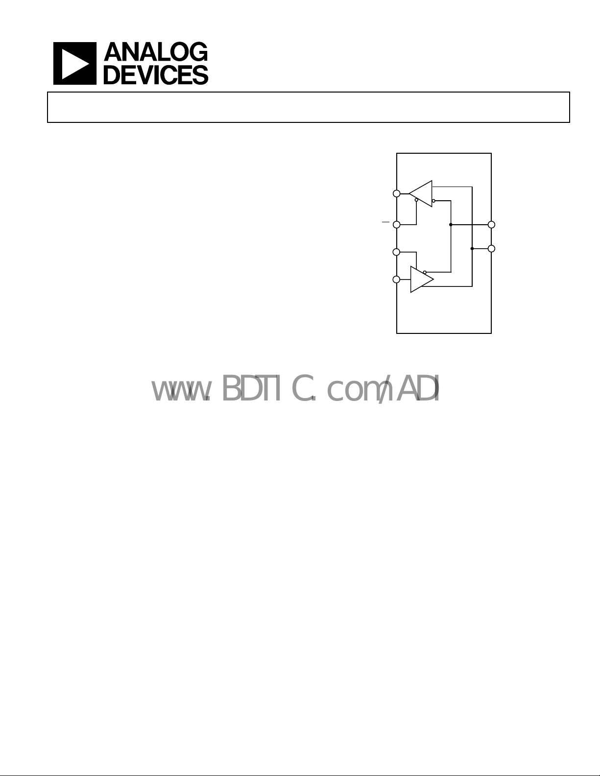
EIA RS-485/RS-422 Transceiver
ADM3485E
FUNCTIONAL BLOCK DIAGRAM
ADM3485E
RO
RE
DE
DI
R
D
Figure 1.
B
A
03338-001
GENERAL DESCRIPTION
The ADM3485E is a 3.3 V, low power data transceiver with
±15 kV ESD protection, suitable for half-duplex communication on multipoint bus transmission lines. The ADM3485E is
designed for balanced data transmission and complies with
TIA/EIA standards RS485 and RS-422. The ADM3485E is
a half-duplex transceiver that shares differential lines and
has separate enable inputs for the driver and the receiver.
The devices have a 12 kΩ receiver input impedance,
h allows up to 32 transceivers on a bus. Because only
whic
one driver should be enabled at any time, the output of a
disabled or powered-down driver is tristated to avoid
overloading the bus.
The receiver has a fail-safe feature that ensures a logic high
o
utput when the inputs are floating. Excessive power dissipation
caused by bus contention or by output shorting is prevented
with a thermal shutdown circuit.
The part is fully specified over the industrial temperature range
a
nd is available in an 8-lead narrow SOIC package.
Rev. C
Information furnished by Analog Devices is believed to be accurate and reliable. However, no
responsibility is assumed by Anal og Devices for its use, nor for any infringements of patents or ot her
rights of third parties that may result from its use. Specifications subject to change without notice. No
license is granted by implication or otherwise under any patent or patent rights of Analog Devices.
Trademarks and registered trademarks are the property of their respective owners.
One Technology Way, P.O. Box 9106, Norwood, MA 02062-9106, U.S.A.
Tel: 781.329.4700 www.analog.com
Fax: 781.461.3113 ©2006 Analog Devices, Inc. All rights reserved.

ADM3485E
www.BDTIC.com/ADI
TABLE OF CONTENTS
Features .............................................................................................. 1
Applications....................................................................................... 1
Functional Block Diagram .............................................................. 1
General Description......................................................................... 1
Revision History ............................................................................... 2
Specifications..................................................................................... 3
Timing Specifications....................................................................... 4
Absolute Maximum Ratings............................................................ 5
Thermal Resistance ...................................................................... 5
ESD Caution.................................................................................. 5
Pin Configuration and Pin Function Descriptions...................... 6
REVISION HISTORY
12/06—Rev. B to Rev. C
Updated Format..................................................................Universal
Removed PDIP Model ....................................................... Universal
Changes to Features, Applications, and General Description .... 1
Changes to Specifications................................................................ 3
Changes to Timing Specifications.................................................. 4
Changes to Absolute Maximum Ratings....................................... 5
Reorganized Test Circuits and Switching
C
haracteristics Section..................................................................... 7
Replaced Figure 3 to Figure 11 ....................................................... 7
Deleted Figure 12 to Figure 14........................................................ 8
Changes to Figure 15 to Figure 20.................................................. 9
Changes to Figure 21 and Figure 22............................................. 10
Changes to Table 9.......................................................................... 11
Deleted Figure 24............................................................................ 11
Removed Fast Transient Burst Immunity
(IEC1000-4-4) S
Updated Outline Dimensions....................................................... 13
Changes to Ordering Guide.......................................................... 13
10/04—Rev. A to Rev. B
Updated Format..................................................................Universal
Changes to Power-Supply Current, Table 1 .................................. 3
Updated Outline Dimensions....................................................... 14
Changes to Ordering Guide.......................................................... 14
5/00—Rev. 0 to Rev. A
ection ................................................................... 12
Test Circuits and Switching Characteristics...................................7
Typical Perf or m an c e Charac t e r istics ..............................................9
Standards and Testing .................................................................... 11
ESD Testing ................................................................................. 11
Applications Information.............................................................. 12
Differential Data Transmission ................................................ 12
Cable and Data Rate................................................................... 12
Receiver Open-Circuit Fail-Safe............................................... 12
Outline Dimensions ....................................................................... 13
Ordering Guide .......................................................................... 13
Rev. C | Page 2 of 16
ADM3485E
www.BDTIC.com/ADI
SPECIFICATIONS
VCC = +3.3 V ± 0.3 V. All specifications T
Table 1.
Parameter Symbol Min Typ Max Unit Test Conditions/Comments
DRIVER
Differential Outputs
Differential Output Voltage V
1.5 V RL = 54 Ω (RS-485) (see Figure 3)
1.5 V RL = 60 Ω (RS-485) (see Figure 4)
∆|VOD| for Complementary Output States1∆V
Common-Mode Output Voltage V
∆|VOC| for Complementary Output States1∆V
Short-Circuit Output Current I
250 mA V
Logic Inputs
Input High Voltage V
Input Low Voltage V
Logic Input Current I
RECEIVER
Differential Inputs
Differential Input Threshold Voltage V
Input Voltage Hysteresis ∆V
Input Resistance (A, B) R
Input Current (A, B) I
–0.8 mA DE = 0 V, VCC = 0 V or 3.6 V, VIN = –7 V
RO Logic Output
Output Voltage High V
Output Voltage Low V
Short-Circuit Output Current I
Tristate Output Leakage Current I
POWER SUPPLY CURRENT
Voltage Range V
Supply Current I
Shutdown Current I
ESD PROTECTION
A, B Pins ±15 kV Human body model
All Pins Except A, B ±4 kV Human body model
1
Δ|VOD| and Δ|VOC| are the changes in VOD and VOC, respectively, when DI input changes state.
MIN
to T
, unless otherwise noted.
MAX
OD
OD
OC
OC
OSD
IH
IL
IN1
TH
TH
IN
IN2
OH
OL
OSR
OZR
CC
CC
2.0 V RL = 100 Ω (RS-422) (see Figure 3)
0.2 V RL = 54 Ω or 100 Ω (see Figure 3)
3 V RL = 54 Ω or 100 Ω ( see Figure 3)
0.2 V RL = 54 Ω or 100 Ω (see Figure 3)
–250 mA V
0.8 V
2.0 V
±2 μA
–0.2 +0.2 V –7 V < VCM < +12 V
50 mV VCM = 0 V
12 kΩ –7 V < VCM < +12 V
1.0 mA DE = 0 V, VCC = 0 V or 3.6 V, VIN = 12 V
VCC – 0.4 V V I
0.4 V I
±8 ±60 mA 0 V < VRO < V
±1 μA VCC = 3.6 V, 0 V < V
3.0 3.6 V
1.1 2.2 mA
0.95 1.9 mA
SHDN
0.002 1 μA
= –7 V
OUT
= 12 V
OUT
DE, DI, RE
DE, DI, RE
DE, DI, RE
= –1.5 mA, VID = 200 mV (see Figure 5)
OUT
= 2.5 mA, VID = 200 mV (see Figure 5)
OUT
CC
< V
OUT
CC
No load, DI = 0 V or V
= 0 V or V
RE
CC
No load, DI = 0 V or V
= 0 V
RE
DE = 0 V, RE
= VCC, DI = 0 V or V
, DE = VCC,
CC
, DE = 0 V,
CC
CC
Rev. C | Page 3 of 16
ADM3485E
www.BDTIC.com/ADI
TIMING SPECIFICATIONS
VCC = 3.3 V, TA = 25°C.
Table 2.
Parameter Symbol Min Typ Max Unit Test Conditions/Comments
DRIVER
Maximum Data Rate 12 15
Differential Output Delay t
Differential Output Transition Time t
DD
TD
Propagation Delay
From Low to High Level t
From High to Low Level t
|t
− t
PLH
| Propagation Delay Skew t
PHL
PLH
PHL
PDS
Enable/Disable Timing
Enable Time to Low Level t
Enable Time to High Level t
Disable Time from Low Level t
Disable Time from High Level t
Enable Time from Shutdown to Low Level t
Enable Time from Shutdown to High Level t
PZL
PZH
PLZ
PHZ
PSL
PSH
RECEIVER
Propagation Delay
From Low to High Level t
From High to Low Level t
|t
− t
RPLH
| Propagation Delay Skew t
RPHL
RPLH
RPHL
RPDS
Enable/Disable Timing
Enable Time to Low Level t
Enable Time to High Level t
Disable Time from Low Level t
Disable Time from High Level t
Enable Time from Shutdown to Low Level t
Enable Time from Shutdown to High Level t
Time to Shutdown
1
The transceivers are put into shutdown mode by bringing the RE high and the DE low. If the inputs are in this state for less than 80 ns, the parts are guaranteed not to
enter shutdown. If the parts are in this state for 300 ns or more, the parts are guaranteed to enter shutdown.
1
t
RPZL
RPZH
RPLZ
RPHZ
RPSL
RPSH
SHDN
1 22 35 ns RL = 60 Ω, CL1 = CL2 = 15 pF (see Figure 6)
3 11 25 ns RL = 60 Ω, CL1 = CL2 = 15 pF (see Figure 6)
7 23 35 ns RL = 27 Ω (see Figure 7)
7 23 35 ns RL = 27 Ω (see Figure 7)
–1.4 ±8 ns RL = 27 Ω (see Figure 7)
42 90 ns RL = 110 Ω (see Figure 9)
42 90 ns RL = 110 Ω (see Figure 8)
35 80 ns RL = 110 Ω (see Figure 9)
35 80 ns RL = 110 Ω (see Figure 8)
650 900 ns RL = 110 Ω (see Figure 9)
650 900 ns RL = 110 Ω (see Figure 8)
25 62 90 ns VID = 0 V to 3.0 V, CL = 15 pF (see Figure 10)
25 62 90 ns VID = 0 V to 3.0 V, CL = 15 pF (see Figure 10)
6 ±10 ns VID = 0 V to 3.0 V, CL = 15 pF (see Figure 10)
25 50 ns CL = 15 pF (see Figure 11)
25 50 ns CL = 15 pF (see Figure 11)
25 45 ns CL = 15 pF (see Figure 11)
25 45 ns CL = 15 pF (see Figure 11)
720 1400 ns CL = 15 pF (see Figure 11)
720 1400 ns CL = 15 pF (see Figure 11)
80 190 300 ns
Rev. C | Page 4 of 16
ADM3485E
www.BDTIC.com/ADI
ABSOLUTE MAXIMUM RATINGS
TA = 25°C, unless otherwise noted.
Table 3.
Parameter Values
VCC to GND –0.3 V to +6 V
Digital Input/Output Voltage (DE, RE, DI)
Receiver Output Voltage (RO) –0.3 V to (VCC + 0.3 V)
Driver Output (A, B)/
Receiver Input (A, B) Voltage −8 V to +13 V
Driver Output Current ±250 mA
Power Dissipation (8-Lead SOIC_N) 650 mW
Operating Temperature Range –40°C to +85°C
Storage Temperature Range –65°C to +150°C
Lead Temperature, Soldering (10 sec) 300°C
Vapor Phase (60 sec) 215°C
Infrared (15 sec) 220°C
ESD Rating
Human Body Model (A, B) ±15 kV
Stresses above those listed under Absolute Maximum Ratings
may cause permanent damage to the device. This is a stress
rating only; functional operation of the device at these or any
other conditions above those indicated in the operational
section of this specification is not implied. Exposure to absolute
maximum rating conditions for extended periods may affect
device reliability.
–0.3 V to +6 V
THERMAL RESISTANCE
θJA is specified for the worst-case conditions, that is, a device
soldered in a circuit board for surface-mount packages.
Table 4. Thermal Resistance
Package Type θ
8-Lead SOIC_N 158 °C/W
JA
Unit
ESD CAUTION
Rev. C | Page 5 of 16

ADM3485E
www.BDTIC.com/ADI
PIN CONFIGURATION AND PIN FUNCTION DESCRIPTIONS
RO
1
ADM3485E
RE
2
TOP VIEW
DE
3
(Not to Scale)
4
DI
Figure 2. SOIC_N Pin Configuration (R-8)
Table 5. Pin Function Descriptions
Pin
Mnemonic
Number
Description
RO 1 Receiver Output. When enabled, if A > B by 200 mV, then RO = high. If A < B by 200 mV, then RO = low.
RE
2
Receiver Output Enable. With RE
low, the receiver output (RO) is enabled. With RE high, the output goes into a
high impedance state. If RE is high and DE is low, the ADM3485E enters a shutdown state.
DE 3
Driver Output Enable. A high level enables the driver differen
impedance state.
DI 4
Driver Input. When the driver is enabled, a logic low on DI forces A low and B high, while a logic high on DI
orces A high and B low.
f
GND 5 Ground Connection, 0 V.
A 6 Noninverting Receiver Input A/Driver Output A.
B 7 Inverting Receiver Input B/Driver Output B.
V
CC
8 Power Supply, 3.3 V ± 0.3 V.
V
8
CC
B
7
A
6
5
GND
03338-002
tial outputs A and B. A low level places it in a high
Rev. C | Page 6 of 16

ADM3485E
V
V
2
www.BDTIC.com/ADI
TEST CIRCUITS AND SWITCHING CHARACTERISTICS
A
/2
R
V
B
L
OD
RL/2
V
Figure 3. Driver Differential Output Voltage and
Co
mmon-Mode Output Voltage
375
D
V
CC
R
V
L
OD
375
Figure 4. Driver Differential Output Voltage with
V
arying Common-Mode Voltage
R
ID
0
V
OL
Figure 5. Receiver Output Voltag
I
OL
(+)
e High and Output Voltage Low
OC
03338-037
VCM =
–7V TO +12V
V
OH
S1
D
GENERATOR
1
PPR = 250kHz, 50% DUT Y CYCLE,
2
CL INCLUDES PROBE AND STRAY CAPACITANCE.
03338-038
OUT
I
OH
(–)
03338-039
OUT
1
50
V
CC
+ V
V
OH
=
V
OM
t
6.0ns, ZO = 50.
R
IN
A
B
1.5V 1.5V
t
PLH
V
OM
t
PHL
V
OM
Figure 7. Driver Propagation Delays
OM
RL = 27
OUT
2
C
= 15pF
L
OL
1.5V
2
3V
0V
t
PHL
V
V
OM
V
OM
OH
V
OL
t
PLH
V
OH
V
OL
03338-041
C
L
RL =
D
GENERATOR
1
PPR = 250kHz, 50% DUTY CYCLE,
2
CL INCLUDES PROBE AND STRAY CAPACITANCE.
IN
OUT
1
50
V
CC
+1.5V +1.5V
t
DD
t
TD
t
6.0ns, ZO = 50.
R
90%90%
50%50%
10%10%
CL = 15pF
t
DD
t
TD
60
+3V
0V
+2V
–2V
2
OUT
03338-040
Figure 6. Driver Differential Output Delay and Transition Times
OM
D
t
PHZ
S1
C
= 50pF
L
+ V
V
OH
V
=
OM
t
6.0ns, ZO = 50.
R
1.5V1.5V
2
2
0V OR 3V
OUT
1
50
IN
t
PZH
V
GENERATOR
1
PPR = 250kHz, 50% DUTY CYCLE ,
CL INCLUDES PRO BE AND STRAY CAPACI TANCE.
Figure 8. Driver Enable and Disable Times (t
OL
0.25V
1.5V
PZH
, t
OUT
RL = 110
3V
0V
V
OH
0V
, t
PSH
PHZ
03338-042
)
Rev. C | Page 7 of 16

ADM3485E
V
2
www.BDTIC.com/ADI
CC
0V OR 3V
OUT
1
50
IN
1.5V 1.5V
V
OM
GENERATOR
1
PPR = 250kHz, 50% DUT Y CYCLE,
2
CL INCLUDES PROBE AND STRAY CAPACIT ANCE.
S1
D
2
C
= 50pF
L
t
6.0ns, ZO = 50.
R
t
PSL
t
Figure 9. Driver Enable and Disable Times (t
+1.5V
–1.5V
GENERATOR
PLZ
0.25V
RL = 110
, t
PZL
S3
OUT
GENERATOR
1
PPR = 250kHz, 50% DUTY CYCLE,
CL INCLUDES PROBE AND STRAY CAPACITANCE.
3V
0V
V
CC
V
OL
PSL
03338-043
, t
)
PLZ
V
R
ID
1
50
1k
2
C
L
OUT
1
1.5V
0V
IN
t
RPLH
Figure 10. Receiver Propagation Delays
S1
S2
50
V
V
V
ID
t
R
1.5V1.5V
OM
CC
OUT
R
C
VOM =
6.0ns, ZO = 50.
t
RPHL
V
OM
= 15pF
L
V
CC
2
3V
0V
V
CC
0V
2
03338-044
1
OUT
OUT
IN
IN
+0.25V
PPR = 250kHz, 50% DUTY CYCLE,
2
CL INCLUDES PROBE AND STRAY CAPACIT ANCE.
+3V
+1.5V
0V
V
0V
+3V
0V
V
0V
OH
OH
+1.5V
t
RPZH
t
RPSH
t
+1.5V
RPHZ
t
R
S1 OPEN
S2 CLOSED
S3 = +1.5V
S1 OPEN
S2 CLOSED
S3 = +1.5V
6.0ns, ZO = 50.
IN
OUT
IN
OUT
+0.25V
+1.5V
t
RPLZ
t
t
RPZL
RPSL
+1.5V
+1.5V
+3V
0V
V
V
+3V
0V
V
V
CC
OL
CC
OL
S1 CLOSED
S2 OPEN
S3 = –1.5V
S1 CLOSED
S2 OPEN
S3 = –1.5V
03338-045
Figure 11. Receiver Enable and Disable Times
Rev. C | Page 8 of 16
ADM3485E
–
www.BDTIC.com/ADI
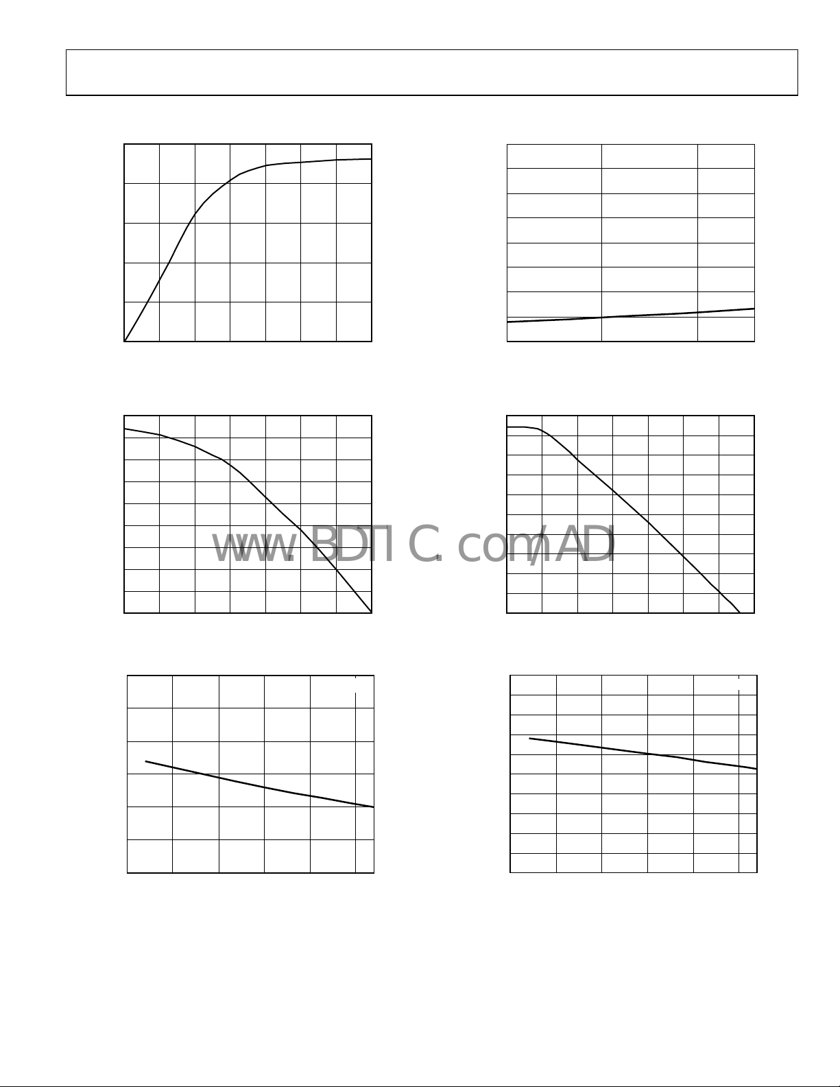
TYPICAL PERFORMANCE CHARACTERISTICS
25
20
0.8
0.7
0.6
IRO = 2.5mA
15
10
OUTPUT CURRENT ( mA)
5
0
03
0.5 1.0 1. 5 2 .0 2.5 3. 0
OUTPUT LOW VOLTAGE (V)
Figure 12. Output Current vs. R
18
–16
–14
–12
–10
–8
–6
OUTPUT CURRENT ( mA)
–4
–2
0
03
0.5 1.0 1. 5 2 .0 2.5 3. 0
OUTPUT HIGH VOLT AGE (V)
Figure 13. Output Current vs. R
3.30
3.25
3.20
3.15
3.10
OUTPUT HIGH VOLT AGE (V)
3.05
3.00
–50 –25 0 25 50 75
eceiver Output Low Voltage
eceiver Output High Voltage
IRO = –1.5mA
TEMPERATURE ( °C)
.5
03338-051
.5
03338-052
03338-053
Figure 14. Receiver Output High Voltage vs. Temperature
0.5
0.4
0.3
0.2
OUTPUT LOW VOLTAGE (V)
0.1
0
–40 10 60 85
Figure 15. Receiver Output Low Voltage vs. Temperature
100
90
80
70
60
50
40
30
OUTPUT CURRENT ( mA)
20
10
0
03.5
0.5 1.0 1. 5 2 .0 2.5 3. 0
Figure 16. Driver Output Current vs. Differential Output Voltage
2.6
2.5
2.4
2.3
2.2
2.1
2.0
1.9
1.8
DIFFERENT IAL OUTPUT VOLT AGE (V)
1.7
1.6
–50
–25 0 25 50 75
Figure 17. Driver Differential Output Voltage vs. Temperature
TEMPERATURE (°C)
DIFFERENT IAL OUT PUT VOL TAGE (V)
TEMPERATURE (° C)
RL = 54
03338-054
03338-055
03338-056
Rev. C | Page 9 of 16

ADM3485E
CH1C
www.BDTIC.com/ADI
120
100
80
60
40
OUTPUT CURRENT (mA)
20
0
024681012
OUTPUT LOW VOLTAGE (V)
Figure 18. Output Current vs. Driv
120
100
80
er Output Low Voltage
03338-057
0.9
0.8
0.7
0.6
0.5
0.4
0.3
SHUTDOWN CURRENT (µA)
0.2
0.1
0
–50
–25 0 25 50 75
TEMPERATURE (° C)
03338-060
Figure 21. Shutdown Current vs. Temperature
DI
3
60
40
OUTPUT CURRENT (mA)
20
0
–7–6–5–4–3–2–101234
OUTPUT HIG H VOLTAG E (V)
Figure 19. Output Current vs. Driv
1.2
1.1
1.0
0.9
0.8
0.7
SUPPLY CURRENT (mA)
0.6
0.5
–40
–10 20 50 80
TEMPERATURE (° C)
er Output High Voltage
Figure 20. Supply Current vs. Temperature
03338-058
03338-059
A
B
H2
CH1 1.0V CH2 1.0V IT 400ps/pt
CH3 2.0V M20ns 1. 25GS/s
Figure 22. Driver Propagation Delay
VA– V
B
M1
RO
3
CH3 2.0V 4ns/ pt
MATH1 2.01V 200ns
M200ns 250MS/ s A CH2 1.24V
Figure 23. Receiver Propagation Delay,
en by External RS-485 Device
Driv
A CH3 1.44V
03338-061
03338-062
Rev. C | Page 10 of 16

ADM3485E
3
www.BDTIC.com/ADI
STANDARDS AND TESTING
Tabl e 6 compares RS-422 and RS-485 interface standards, and
Tabl e 7 and Ta b le 8 show transmitting and receiving truth tables.
Table 6.
Specification RS-422 RS-485
Transmission Type Differential Differential
Maximum Data Rate 10 Mbps 10 Mbps
Maximum Cable Length 4000 ft 4000 ft
Minimum Driver Output Voltage ±2 V ±1.5 V
Driver Load Impedance 100 Ω 54 Ω
Receiver Input Resistance 4 kΩ min 12 kΩ min
Receiver Input Sensitivity ±200 mV ±200 mV
Receiver Input Voltage Range −7 V to +7 V −7 V to +12 V
Number of Drivers/Receivers per Line 1/10 32/32
Table 7. Transmitting Truth Table
Transmitting Inputs Transmitting Outputs
RE
1
X
1
X
0 0 X
1 0 X
1
X = don't care.
2
High-Z = high impedance.
DE DI B A
1 1 0 1
1 0 1 0
1
1
High-Z
High-Z
2
2
High-Z
High-Z
2
2
Table 8. Receiving Truth Table
Receiving Inputs Receiving Outputs
RE
0 X
0 X
0 X
1 X
1
X = don't care.
2
High-Z = high impedance.
DE A – B RO
1
1
1
1
> +0.2 V 1
< –0.2 V 0
Inputs open 1
1
X
High-Z
2
influenced by humidity, temperature, barometric pressure,
distance, and rate of closure of the discharge gun. The contact
discharge method, while less realistic, is more repeatable and is
gaining acceptance and preference over the air-gap method.
Although very little energy is contained within an ESD pulse,
t
he extremely fast rise time, coupled with high voltages, can
cause failures in unprotected semiconductors. Catastrophic
destruction can occur immediately as a result of arcing or
heating. Even if catastrophic failure does not occur immediately,
the device can suffer from parametric degradation, which can
result in degraded performance. The cumulative effects of
continuous exposure can eventually lead to complete failure.
I/O lines are particularly vulnerable to ESD damage. Simply
tou
ching or plugging in an I/O cable can result in a static
discharge that can damage or completely destroy the interface
product connected to the I/O port. It is extremely important,
therefore, to have high levels of ESD protection on the I/O lines.
The ESD discharge could induce latch-up in the device under
st, so it is important that ESD testing on the I/O pins be
te
carried out while device power is applied. This type of testing is
more representative of a real-world I/O discharge, where the
equipment is operating normally when the discharge occurs.
Table 9. ESD Test Results
ESD Test Method I/O Pins
Human Body Model ±15 kV
100%
90%
PEAK
I
ESD TESTING
Two coupling me t hods are us e d for ESD testi n g , cont act
discharge and air-gap discharge. Contact discharge calls for a
direct connection to the unit being tested. Air-gap discharge
uses a higher test voltage but does not make direct contact with
the unit under test. With air-gap discharge, the discharge gun is
moved toward the unit under test, developing an arc across the
air gap, hence the term air-gap discharge. This method is
Rev. C | Page 11 of 16
6.8%
10%
t
RL
Figure 24. Human Body Model Current Waveform
t
DL
TIME
t
03338-023

ADM3485E
www.BDTIC.com/ADI
APPLICATIONS INFORMATION
DIFFERENTIAL DATA TRANSMISSION
Differential data transmission is used to reliably transmit data
at high rates over long distances and through noisy environments. Differential transmission nullifies the effects of ground
shifts and noise signals that appear as common-mode voltages
on the line.
Two main standards that specify the electrical characteristics of
nsceivers used in differential data transmission are approved
tra
by the Electronics Industries Association (EIA). The RS-422
standard specifies data rates up to 10 Mbps and line lengths up
to 4000 feet. A single driver can drive a transmission line with
up to 10 receivers. The RS-485 standard was defined to cater to
true multipoint communications. This standard meets or
exceeds all the requirements of RS-422 but also allows multiple
drivers and receivers to be connected to a single bus. An
extended common-mode range of −7 V to +12 V is defined.
The most significant difference between RS-422 and RS-485 is
e fact that under the RS-485 standard the drivers may be
th
disabled, thereby allowing more than one to be connected to a
single line. Only one driver should be enabled at a time, but the
RS-485 standard contains additional specifications to guarantee
device safety in the event of line contention.
CABLE AND DATA RATE
The transmission line of choice for RS-485 communications is a
twisted pair. Twisted-pair cable tends to cancel common-mode
noise and also causes cancellation of the magnetic fields
generated by the current flowing through each wire, thereby
reducing the effective inductance of the pair.
The ADM3485E is designed for bidirectional data communi-
ations on multipoint transmission lines. A typical application
c
showing a multipoint transmission network is illustrated in
Figure 25. Only one driver can transmit at a particular time,
b
ut multiple receivers may be enabled simultaneously.
As with any transmission line, it is important that reflections are
minimize
d. This can be achieved by terminating the extreme
ends of the line using resistors equal to the characteristic impedance of the line. Stub lengths off the main line must also be
kept as short as possible. A properly terminated transmission
line appears purely resistive to the driver.
RECEIVER OPEN-CIRCUIT FAIL-SAFE
The receiver input includes a fail-safe feature that guarantees
a logic high on the receiver when the inputs are open circuit
or floating.
Table 10. RS-422 and RS-485 Interface Standards
Specification RS-422 RS-485
Transmission Type Differential Differential
Maximum Cable Length 4000 ft 4000 ft
Minimum Driver Output Voltage ±2 V ±1.5 V
Driver Load Impedance 100 Ω 54 Ω
Receiver Input Resistance 4 kΩ min 12 kΩ min
Receiver Input Sensitivity ±200 mV ±200 mV
Receiver Input Voltage Range
−7 V to +7 V −7 V to +12 V
ADM3485E
A
B
R
RO
RE
DE
D
DI
03338-027
RO
RE
DE
DI
ADM3485E
R
D
A
B
ADM3485E
R
RO
A
B
D
DE
RE DI
MAXIMUM NUMBER OF TRANSCEIVERS ON BUS: 50
Figure 25. Multipoint Transmission Network
RO
A
R
RE
B
ADM3485E
D
DI
DE
Rev. C | Page 12 of 16
ADM3485E
www.BDTIC.com/ADI
OUTLINE DIMENSIONS
5.00 (0.1968)
4.80 (0.1890)
4.00 (0.1574)
3.80 (0.1497)
0.25 (0.0098)
0.10 (0.0040)
COPLANARIT Y
0.10
CONTROLL ING DIM ENSIONS ARE IN MILL IMETERS; INCH DIME NSIONS
(IN PARENTHESES) ARE ROUNDE D-OFF M ILLIMETER EQUIVALENTS FOR
REFERENCE ON LY AND ARE NOT APPRO PRIATE FOR US E IN DESIG N.
85
1
1.27 (0.0500)
SEATING
PLANE
COMPLI ANT TO JEDEC STANDARDS MS-012-A A
Figure 26. 8-Lead Standard Small Outline Package [SOIC_N]
BSC
6.20 (0.2440)
5.80 (0.2284)
4
1.75 (0.0688)
1.35 (0.0532)
0.51 (0.0201)
0.31 (0.0122)
Nar
row Body
8°
0°
0.25 (0.0098)
0.17 (0.0067)
0.50 (0.0196)
0.25 (0.0099)
1.27 (0.0500)
0.40 (0.0157)
45°
060506-A
(R-8)
Dimensions shown in millimeters and (inches)
ORDERING GUIDE
Model Temperature Range Package Description Package Option
ADM3485EAR –40°C to +85°C 8-Lead Standard Small Outline Package [SOIC_N] R-8
ADM3485EAR-REEL7 –40°C to +85°C 8-Lead Standard Small Outline Package [SOIC_N] R-8
ADM3485EAR-REEL –40°C to +85°C 8-Lead Standard Small Outline Package [SOIC_N] R-8
ADM3485EARZ
ADM3485EARZ-REEL7
ADM3485EARZ-REEL
1
Z = Pb-free part.
1
1
1
–40°C to +85°C 8-Lead Standard Small Outline Package [SOIC_N] R-8
–40°C to +85°C 8-Lead Standard Small Outline Package [SOIC_N] R-8
–40°C to +85°C 8-Lead Standard Small Outline Package [SOIC_N] R-8
Rev. C | Page 13 of 16

ADM3485E
www.BDTIC.com/ADI
NOTES
Rev. C | Page 14 of 16

ADM3485E
www.BDTIC.com/ADI
NOTES
Rev. C | Page 15 of 16

ADM3485E
www.BDTIC.com/ADI
NOTES
©2006 Analog Devices, Inc. All rights reserved. Trademarks and
registered trademarks are the property of their respective owners.
C03338-0-12/06(C)
T
Rev. C | Page 16 of 16
TTT
 Loading...