

现货库存、技术资料、百科信息、热点资讯,精彩尽在鼎好!
V
V
V
3.3 V, ±15 kV ESD-Protected, Half- and
Full-Duplex, RS-485/RS-422 Transceivers
ADM3483E/ADM3486E/ADM3488E/ADM3490E/ADM3491E
FEATURES
TIA/EIA RS-485/RS-422 compliant
±15 kV ESD protection on RS-485 input/output pins
Data rates
ADM3483E/ADM3488E: 250 kbps
ADM3486E: 2.5 Mbps
ADM3490E/ADM3491E: 12 Mbps
Half- and full-duplex options
Up to 32 nodes on the bus
Receiver open-circuit, fail-safe design
Low power shutdown current
(ADM3483E/ADM3486E/ADM3491E only)
Outputs high-Z when disabled or powered off
Common-mode input range: −7 V to +12 V
Thermal shutdown and short-circuit protection
Industry-standard 75176 pinout
8-lead and 14-lead narrow SOIC packages
APPLICATIONS
Power/energy metering
Telecommunications
EMI-sensitive systems
Industrial control
Local area networks
GENERAL DESCRIPTION
The ADM3483E/ADM3486E/ADM3488E/ADM3490E/
ADM3491E are 3.3 V, low power data transceivers with
±15 kV ESD protection suitable for full- and half-duplex
communication on multipoint bus transmission lines. They
are designed for balanced data transmission, and they
comply with TIA/EIA standards RS485 and RS-422. The
ADM3483E/ADM3486E are half-duplex transceivers that
share differential lines and have separate enable inputs for
the driver and receiver. The full-duplex ADM3488E/
ADM3490E/ADM3491E transceivers have dedicated
differential line driver outputs and receiver inputs. The
ADM3491E also features separate enable inputs for the
driver and receiver.
The devices have a 12 kΩ receiver input impedance,
which allows up to 32 transceivers on a bus. Because only
one driver should be enabled at any time, the output of a
disabled or powered-down driver is tristated to avoid
overloading the bus.
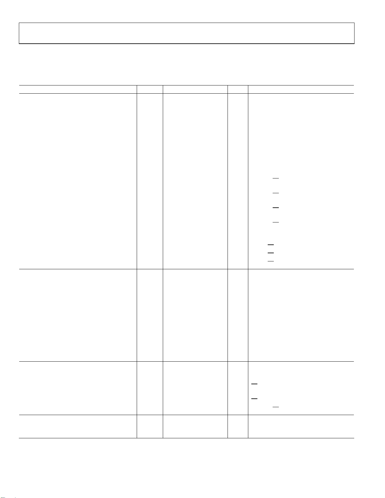
FUNCTIONAL BLOCK DIAGRAMS
CC
ADM3483E/
ADM3486E
RO
RE
DE
DI
RO
DI
RO
RE
DE
DI
R
D
GND
Figure 1.
CC
ADM3488E/
ADM3490E
R
D
GND
Figure 2.
CC
ADM3491E
R
D
GND
Figure 3.
A
B
6284-001
A
B
Z
Y
6284-002
A
B
Z
Y
06284-003
(continued on Page 3)
Rev. A
Information furnished by Analog Devices is believed to be accurate and reliable. However, no
responsibility is assumed by Anal og Devices for its use, nor for any infringements of patents or ot her
rights of third parties that may result from its use. Specifications subject to change without notice. No
license is granted by implication or otherwise under any patent or patent rights of Analog Devices.
Trademarks and registered trademarks are the property of their respective owners.
One Technology Way, P.O. Box 9106, Norwood, MA 02062-9106, U.S.A.
Tel: 781.329.4700 www.analog.com
Fax: 781.461.3113 ©2006 Analog Devices, Inc. All rights reserved.

ADM3483E/ADM3486E/ADM3488E/ADM3490E/ADM3491E
TABLE OF CONTENTS
Features.............................................................................................. 1
Applications....................................................................................... 1
General Description ......................................................................... 1
Functional Block Diagrams............................................................. 1
Revision History ............................................................................... 2
Specifications..................................................................................... 4
Driver Timing Specifications...................................................... 5
Receiver Timing Specifications .................................................. 6
Absolute Maximum Ratings............................................................ 7
ESD Caution.................................................................................. 7
Pin Configurations and Function Descriptions ........................... 8
Test Circuits and Switching Characteristics.................................. 9
Typical Performance Characteristics ........................................... 11
Circuit Description......................................................................... 14
Devices with Receiver/Driver Enable—ADM3483E/
ADM3486E/ ADM3491E ........................................................... 14
Devices Without Receiver/Driver Enable― ADM3488E/
ADM3490E ................................................................................. 14
Low Power Shutdown Mode—ADM3483E/ ADM3486E/
ADM3491E ................................................................................. 14
Driver Output Protection.......................................................... 14
Propagation Delay...................................................................... 14
Line Length vs. Data Rate ......................................................... 14
±15 kV ESD Protection ............................................................. 15
Human Body Model .................................................................. 15
Typical Applications................................................................... 15
Outline Dimensions....................................................................... 18
Ordering Guide .......................................................................... 18
REVISION HISTORY
10/06—Rev. 0 to Rev. A
Added ADM3483E and ADM3488E ...............................Universal
Changes to Figure 1 and Figure 2................................................... 1
Inserted Table 3................................................................................. 5
Changes to Figure 4 and Figure 5................................................... 8
Inserted Figure 28 and Figure 29.................................................. 13
Changes to Figure 31 and Figure 32............................................. 16
Changes to Figure 34...................................................................... 17
Updated Outline Dimensions....................................................... 18
Changes to Ordering Guide.......................................................... 18
8/06—Revision 0: Initial Version
Rev. A | Page 2 of 20

ADM3483E/ADM3486E/ADM3488E/ADM3490E/ADM3491E
GENERAL DESCRIPTION
(continued from Page 1)
The driver outputs of the ADM3483E/ADM3486E/
ADM3488E are slew rate limited, in order to reduce EMI
and data errors caused by reflections from improperly
terminated buses. The receiver has a fail-safe feature that
ensures a logic high output when the inputs are floating.
Table 1. Selection Table
Guaranteed Data
Part No.
ADM3483E 0.25 3.0 to 3.6 Half Yes Yes Yes 8
ADM3486E 2.5 3.0 to 3.6 Half Yes Yes Yes 8
ADM3488E 0.25 3.0 to 3.6 Full Yes No Yes 8
ADM3490E 12 3.0 to 3.6 Full No No Yes 8
ADM3491E 12 3.0 to 3.6 Full No Yes Yes 14
Rate (Mbps)
Supply
Voltage (V)
Half/Full
Duplex
Slew Rate
Limited
Excessive power dissipation caused by bus contention
or by output shorting is prevented with a thermal shutdown circuit.
The parts are fully specified over the industrial temperature range
and are available in 8-lead and 14-lead narrow SOIC packages.
Driver/Receiver
Enable
±15 kV ESD Protection
on Bus Pins
Pin Count
Rev. A | Page 3 of 20
ADM3483E/ADM3486E/ADM3488E/ADM3490E/ADM3491E
SPECIFICATIONS
VCC = 3.3 V ± 0.3 V, TA = T
Table 2. ADM3483E/ADM3486E/ADM3488E/ADM3490E/ADM3491E
Parameter Symbol Min Typ Max Unit Test Conditions/Comments
DRIVER
Differential Outputs
Differential Output Voltage VOD 2.0 V RL = 100 Ω (RS-422) (see Figure 7)
1.5 V RL = 54 Ω (RS-485) (see Figure 7)
1.5 V RL = 60 Ω (RS-485) (see Figure 8)
Δ|VOD| for Complementary Output States1 ∆VOD 0.2 V RL = 54 Ω or 100 Ω (see Figure 7)
Common-Mode Output Voltage VOC 3 V RL = 54 Ω or 100 Ω (see Figure 7)
Δ|VOC| for Complementary Output States1 ∆VOC 0.2 V RL = 54 Ω or 100 Ω (see Figure 7)
Short-Circuit Output Current I
250 mA V
Output Leakage (Y, Z) (ADM3491E Only) IO
Normal Mode 20 μA
−20 μA
Shutdown Mode 1 μA
−1 μA
Logic Inputs
Input High Voltage VIH 2.0 V
Input Low Voltage VIL 0.8 V
Logic Input Current I
RECEIVER
Differential Inputs
Differential Input Threshold Voltage VTH −0.2 0.2 V −7 V < VCM < +12 V
Input Hysteresis ∆VTH 50 mV VCM = 0 V
Input Resistance (A, B) RIN 12
Input Current (A, B) I
−0.8 mA DE = 0 V, VCC = 0 V or 3.6 V, VIN = −7 V
RO Logic Output
Output High Voltage VOH V
Output Low Voltage VOL 0.4 V I
Short-Circuit Output Current I
Tristate Output Leakage Current I
POWER SUPPLY
Voltage Range VCC 3.0 3.6 V
Supply Current ICC 1.1 2.2 mA
0.95 1.9 mA
Shutdown Current I
ESD PROTECTION
A, B, Y, Z Pins ±15 kV Human body model
All Pins Except A, B, Y, Z Pins ±4 kV Human body model
1
Δ|VOD| and Δ|VOC| are the changes in VOD and VOC, respectively, when DI input changes state.
MIN
to T
, unless otherwise noted.
MAX
−250 mA V
OSD
±2 μA
IN1
1.0 mA DE = 0 V, VCC = 0 V or 3.6 V, VIN = 12 V
IN2
±8 ±60 mA 0 V < VRO < VCC
OSR
±1 μA VCC = 3.6 V, 0 V < V
OZR
0.002 1 μA
SHDN
kΩ
− 0.4 V I
CC
= −7 V
OUT
= 12 V
OUT
DE = 0 V, RE
V
OUT
DE = 0 V, RE
V
OUT
DE = 0 V, RE
V
OUT
DE = 0 V, RE
V
OUT
DE, DI, RE
DE, DI, RE
DE, DI, RE
= 0 V, VCC = 0 V or 3.6 V,
= 12 V
= 0 V, VCC = 0 V or 3.6 V,
= −7 V
= VCC, VCC = 0 V or 3.6 V,
= 12 V
= VCC, VCC = 0 V or 3.6 V,
= −7 V
−7 V < VCM < +12 V
= −1.5 mA, VID = 200 mV (see Figure 9)
OUT
= 2.5 mA, VID = 200 mV (see Figure 9)
OUT
< VCC
OUT
No load, DI = 0 V or V
= 0 V or VCC
RE
No load, DI = 0 V or V
RE
= 0 V
DE = 0 V, RE
= VCC, DI = 0 V or VCC
, DE = VCC,
CC
, DE = 0 V,
CC
Rev. A | Page 4 of 20
ADM3483E/ADM3486E/ADM3488E/ADM3490E/ADM3491E
DRIVER TIMING SPECIFICATIONS
VCC = 3.3 V, TA = 25°C.
Table 3. ADM3483E/ADM3488E
Parameter Symbol Min Typ Max Unit Test Conditions/Comments
MAXIMUM DATA RATE 250 kbps
DIFFERENTIAL OUTPUT DELAY tDD 600 900 1400 ns RL = 60 Ω (see Figure 10)
DIFFERENTIAL OUTPUT TRANSITION TIME tTD 400 740 1200 ns RL = 60 Ω (see Figure 10)
PROPAGATION DELAY
From Low to High Level t
From High to Low Level t
|t
− t
PLH
| PROPAGATION DELAY SKEW1 t
PHL
ENABLE/DISABLE TIMING (ADM3483E ONLY)
Enable Time to Low Level t
Enable Time to High Level t
Disable Time from Low Level t
Disable Time from High Level t
Enable Time from Shutdown to Low Level t
Enable Time from Shutdown to High Level t
1
Measured on |t
PLH
(Y) − t
(Y)| and |t
PHL
PLH
(Z) − t
(Z)|.
PHL
700 930 1500 ns RL = 27 Ω (see Figure 11)
PLH
700 930 1500 ns RL = 27 Ω (see Figure 11)
PHL
±50 ns RL = 27 Ω (see Figure 11)
PDS
900 1300 ns RL = 110 Ω (see Figure 13)
PZL
600 800 ns RL = 110 Ω (see Figure 12)
PZH
50 80 ns RL = 110 Ω (see Figure 13)
PLZ
50 80 ns RL = 110 Ω (see Figure 12)
PHZ
1.9 2.7 μs RL = 110 Ω (see Figure 13)
PSL
2.2 3.0 μs RL = 110 Ω (see Figure 12)
PSH
VCC = 3.3 V, TA = 25°C.
Table 4. ADM3486E
Parameter Symbol Min Typ Max Unit Test Conditions/Comments
MAXIMUM DATA RATE 2.5 Mbps
DIFFERENTIAL OUTPUT DELAY tDD 20 42 70 ns RL = 60 Ω (see Figure 10)
DIFFERENTIAL OUTPUT TRANSITION TIME tTD 15 28 60 ns RL = 60 Ω (see Figure 10)
PROPAGATION DELAY
From Low to High Level t
From High to Low Level t
|t
− t
PLH
| PROPAGATION DELAY SKEW
PHL
1
20 42 75 ns RL = 27 Ω (see Figure 11)
PLH
20 42 75 ns RL = 27 Ω (see Figure 11)
PHL
t
−6 ±12 ns RL = 27 Ω (see Figure 11)
PDS
ENABLE/DISABLE TIMING
Enable Time to Low Level t
Enable Time to High Level t
Disable Time from Low Level t
Disable Time from High Level t
Enable Time from Shutdown to Low Level t
Enable Time from Shutdown to High Level t
1
Measured on |t
PLH
(Y) − t
(Y)| and |t
PHL
PLH
(Z) − t
(Z)|.
PHL
52 100 ns RL = 110 Ω (see Figure 13)
PZL
52 100 ns RL = 110 Ω (see Figure 12)
PZH
40 80 ns RL = 110 Ω (see Figure 13)
PLZ
40 80 ns RL = 110 Ω (see Figure 12)
PHZ
700 1000 ns RL = 110 Ω (see Figure 13)
PSL
700 1000 ns RL = 110 Ω (see Figure 12)
PSH
Rev. A | Page 5 of 20
ADM3483E/ADM3486E/ADM3488E/ADM3490E/ADM3491E
VCC = 3.3 V, TA = 25°C.
Table 5. ADM3490E/ADM3491E
Parameter Symbol Min Typ Max Unit Test Conditions/Comments
MAXIMUM DATA RATE 12 15 Mbps
DIFFERENTIAL OUTPUT DELAY tDD 1 22 35 ns RL = 60 Ω (see Figure 10)
DIFFERENTIAL OUTPUT TRANSITION TIME tTD 3 11 25 ns RL = 60 Ω (see Figure 10)
PROPAGATION DELAY
From Low to High Level t
From High to Low Level t
|t
− t
PLH
| PROPAGATION DELAY SKEW1 t
PHL
ENABLE/DISABLE TIMING (ADM3491E ONLY)
Enable Time to Low Level t
Enable Time to High Level t
Disable Time from Low Level t
Disable Time from High Level t
Enable Time from Shutdown to Low Level t
Enable Time from Shutdown to High Level t
1
Measured on |t
PLH
(Y) − t
(Y)| and |t
PHL
PLH
(Z) − t
(Z)|.
PHL
RECEIVER TIMING SPECIFICATIONS
VCC = 3.3 V, TA = 25°C.
7 23 35 ns RL = 27 Ω (see Figure 11)
PLH
7 23 35 ns RL = 27 Ω (see Figure 11)
PHL
−1.4 ±8 ns RL = 27 Ω (see Figure 11)
PDS
42 90 ns RL = 110 Ω (see Figure 13)
PZL
42 90 ns RL = 110 Ω (see Figure 12)
PZH
35 80 ns RL = 110 Ω (see Figure 13)
PLZ
35 80 ns RL = 110 Ω (see Figure 12)
PHZ
650 900 ns RL = 110 Ω (see Figure 13)
PSL
650 900 ns RL = 110 Ω (see Figure 12)
PSH
Table 6. ADM3483E/ADM3486E/ADM3488E/ADM3490E/ADM3491E
Parameter Symbol Min Typ Max Unit Test Conditions/Comments
PROPAGATION DELAY
From Low to High Level t
RPLH
ADM3486E/ADM3490E/ADM3491E 25 62 90 ns VID = 0 V to 3.0 V, CL = 15 pF (see Figure 14)
ADM3483E/ADM3488E 25 75 120 ns VID = 0 V to 3.0 V, CL = 15 pF (see Figure 14)
From High to Low Level t
RPHL
ADM3486E/ADM3490E/ADM3491E 25 62 90 ns VID = 0 V to 3.0 V, CL = 15 pF (see Figure 14)
ADM3483E/ADM3488E 25 75 120 ns VID = 0 V to 3.0 V, CL = 15 pF (see Figure 14)
|t
− t
RPLH
| PROPAGATION DELAY SKEW t
RPHL
RPDS
ADM3486E/ADM3490E/ADM3491E +6 ±10 ns VID = 0 V to 3.0 V, CL = 15 pF (see Figure 14)
ADM3483E/ADM3488E +12 ±20 ns VID = 0 V to 3.0 V, CL = 15 pF (see Figure 14)
ENABLE/DISABLE TIMING (ADM3483E/ADM3486E/
ADM3491E ONLY)
Enable Time to Low Level t
Enable Time to High Level t
Disable Time from Low Level t
Disable Time from High Level t
Enable Time from Shutdown to Low Level t
Enable Time from Shutdown to High Level t
Time to Shutdown1 t
1
The transceivers are put into shutdown mode by bringing the RE high and the DE low. If the inputs are in this state for less than 80 ns, the parts are guaranteed not to
enter shutdown. If the parts are in this state for 300 ns or more, the parts are guaranteed to enter shutdown.
25 50 ns CL = 15 pF (see Figure 15)
RPZL
25 50 ns CL = 15 pF (see Figure 15)
RPZH
25 45 ns CL = 15 pF (see Figure 15)
RPLZ
25 45 ns CL = 15 pF (see Figure 15)
RPHZ
720 1400 ns CL = 15 pF (see Figure 15)
RPSL
720 1400 ns CL = 15 pF (see Figure 15)
RPSH
80 190 300 ns
SHDN
Rev. A | Page 6 of 20

ADM3483E/ADM3486E/ADM3488E/ADM3490E/ADM3491E
ABSOLUTE MAXIMUM RATINGS
TA = 25°C, unless otherwise noted.
Table 7.
Parameter Rating
VCC to GND −0.3 V to +6 V
Digital Input/Output Voltage (DE, RE, DI)
Receiver Output Voltage (RO) −0.3 V to (VCC + 0.3 V)
Driver Output (A, B, Y, Z)/Receiver Input
(A, B) Voltage
Driver Output Current ±250 mA
Operating Temperature Range −40°C to +85°C
Storage Temperature Range −65°C to +150°C
θJA Thermal Impedance
8-Lead SOIC_N 158°C/W
14-Lead SOIC_N 120°C/W
Lead Temperature, Soldering (20 sec) 260°C
−0.3 V to +6 V
−8 V to +13 V
Stresses above those listed under Absolute Maximum Ratings
may cause permanent damage to the device. This is a stress
rating only; functional operation of the device at these or any
other conditions above those indicated in the operational
section of this specification is not implied. Exposure to absolute
maximum rating conditions for extended periods may affect
device reliability.
ESD CAUTION
Rev. A | Page 7 of 20

ADM3483E/ADM3486E/ADM3488E/ADM3490E/ADM3491E
PIN CONFIGURATIONS AND FUNCTION DESCRIPTIONS
NC
1
RO
2
RE
3
ADM3491E
DE
4
TOP VIEW
RO
RE
DE
DI
1
ADM3483E/
ADM3486E
2
3
TOP VIEW
(Not to Scale)
4
V
8
CC
B
7
6
A
GND
5
Figure 4. ADM3483E/ADM3486E
Pin Configuration
V
1
CC
ADM3488E/
ADM3490E
2
RO
DI
3
TOP VIEW
(Not to Scal e)
GND
06284-004
4
A
8
7
B
Z
6
Y
5
06284-005
Figure 5. ADM3488E/ADM3490E
Pin Configuration
(Not to Scale)
5
DI
6
GND
GND
7
NC = NO CONNECT
Figure 6. ADM3491E
Pin Configuration
Table 8. Pin Function Descriptions
ADM3483E/
ADM3486E
Pin No.
1 2 2 RO
ADM3488E/
ADM3490E
Pin No.
ADM3491E
Pin No.
Mnemonic Description
Receiver Output. If A > B by 200 mV, RO is high; if A < B by 200 mV,
RO is low.
2 N/A 3
RE Receiver Output Enable. A low level enables the receiver output. A high
level places it in a high impedance state. If RE is high and DE is low, the
device enters a low power shutdown mode.
3 N/A 4 DE
Driver Output Enable. A high level enables the driver differential A and B
outputs. A low level places it in a high impedance state. If
is low, the device enters a low power shutdown mode.
4 3 5 DI
Driver Input. With a half-duplex part when the driver is enabled, a logic low
on DI forces A low and B high; a logic high on DI forces A high and B low.
With a full-duplex part when the driver is enabled, a logic low on DI forces Y
low and Z high; a logic high on DI forces Y high and Z low.
5 4 6, 7 GND Ground.
N/A 5 9 Y Noninverting Driver Output.
6 N/A N/A A Noninverting Receiver Input A and Noninverting Driver Output A.
N/A 8 12 A Noninverting Receiver Input A.
N/A 6 10 Z Inverting Driver Output.
7 N/A N/A B Inverting Receiver Input B and Inverting Driver Output B.
N/A 7 11 B Inverting Receiver Input B.
8 1 13, 14 V
CC
Power Supply, 3.3 V ± 0.3 V. Bypass V
to GND with a 0.1 μF capacitor.
CC
N/A N/A 1, 8 NC No Connect. Not internally connected. Can be connected to GND.
V
14
CC
V
13
CC
A
12
B
11
10
Z
9
Y
NC
8
06284-006
RE is high and DE
Rev. A | Page 8 of 20

ADM3483E/ADM3486E/ADM3488E/ADM3490E/ADM3491E
V
V
2
TEST CIRCUITS AND SWITCHING CHARACTERISTICS
+ V
2
OM
RL = 27
OUT
2
C
= 15pF
L
OL
1.5V
3V
0V
t
PHL
V
V
OM
V
OM
OH
V
OL
t
PLH
V
OH
V
OL
06284-011
Y
/2
R
V
Z
L
OD
RL/2
V
OC
06284-007
Figure 7. Driver Differential Output Voltage and
Common-Mode Output Voltage
375
VCM =
D
V
CC
R
V
OD
L
375
–7V TO +12V
06284-008
Figure 8. Driver Differential Output Voltage with
Varying Common-Mode Voltage
R
ID
0
V
OL
I
V
OL
OH
(+)
I
OH
(–)
06284-009
Figure 9. Receiver Output Voltage High and Output Voltage Low
S1
D
GENERATOR
1
PPR = 250kHz, 50% DUT Y CYCLE,
2
CL INCLUDES PROBE AND STRAY CAPACITANCE.
OUT
OUT
1
50
V
CC
V
OH
=
V
OM
t
6.0ns, ZO = 50.
R
IN
Y
Z
1.5V 1.5V
t
PLH
V
OM
t
PHL
V
OM
Figure 11. Driver Propagation Delays
C
L
RL =
D
GENERATOR
1
PPR = 250kHz, 50% DUTY CYCLE,
2
CL INCLUDES PROBE AND STRAY CAPACITANCE.
1
50
V
CC
CL = 15pF
t
6.0ns, ZO = 50.
R
60
OUT
2
+3V
IN
+1.5V +1.5V
0V
t
DD
+2V
50%50%
10%10%
–2V
t
TD
06284-010
OUT
t
DD
90%90%
t
TD
Figure 10. Driver Differential Output Delay and Transition Times
OM
D
t
PHZ
S1
C
= 50pF
L
V
OH
V
=
OM
t
6.0ns, ZO = 50.
R
1.5V1.5V
2
+ V
2
0V OR 3V
GENERATOR
1
PPR = 250kHz, 50% DUTY CYCLE ,
CL INCLUDES PRO BE AND STRAY CAPACI TANCE.
1
50
IN
t
PZH
OUT
V
Figure 12. Driver Enable and Disable Times (t
OL
0.25V
1.5V
, t
PZH
OUT
RL = 110
3V
0V
V
OH
0V
, t
PSH
PHZ
06284-012
)
Rev. A | Page 9 of 20

ADM3483E/ADM3486E/ADM3488E/ADM3490E/ADM3491E
V
2
CC
0V OR 3V
GENERATOR
1
PPR = 250kHz, 50% DUT Y CYCLE,
2
CL INCLUDES PROBE AND STRAY CAPACIT ANCE.
1
IN
OUT
D
50
1.5V 1.5V
t
PSL
V
OM
Figure 13. Driver Enable and Disable Times (t
S1
2
C
= 50pF
L
t
6.0ns, ZO = 50.
R
t
PLZ
0.25V
+1.5V
–1.5V
RL = 110
, t
PZL
S3
OUT
GENERATOR
1
50
V
ID
1.5V
0V
1
PPR = 250kHz, 50% DUTY CYCLE,
CL INCLUDES PROBE AND STRAY CAPACITANCE.
t
R
3V
0V
V
CC
V
OL
PSL
06284-013
, t
)
PLZ
IN
t
RPLH
OUT
Figure 14. Receiver Propagation Delays
S1
V
R
ID
1k
2
C
L
S2
1.5V1.5V
V
OM
V
CC
OUT
R
C
VOM =
6.0ns, ZO = 50.
t
RPHL
V
OM
= 15pF
L
V
CC
2
3V
0V
V
CC
0V
2
06284-014
OUT
OUT
IN
IN
+0.25V
+1.5V
1
+3V
0V
V
OH
50
t
S1 OPEN
S2 CLOSED
S3 = +1.5V
GENERATOR
1
PPR = 250kHz, 50% DUTY CYCLE,
2
CL INCLUDES PROBE AND STRAY CAPACIT ANCE.
t
RPZH
t
RPSH
+1.5V
0V
+3V
S1 OPEN
0V
V
OH
S2 CLOSED
S3 = +1.5V
+1.5V
t
RPHZ
0V
Figure 15. Receiver Enable and Disable Times
6.0ns, ZO = 50.
R
OUT
OUT
IN
IN
+0.25V
+1.5V
t
RPLZ
t
t
RPZL
RPSL
+1.5V
+1.5V
+3V
0V
V
V
+3V
0V
V
V
CC
OL
CC
OL
S1 CLOSED
S2 OPEN
S3 = –1.5V
S1 CLOSED
S2 OPEN
S3 = –1.5V
06284-015
Rev. A | Page 10 of 20

ADM3483E/ADM3486E/ADM3488E/ADM3490E/ADM3491E
–
TYPICAL PERFORMANCE CHARACTERISTICS
25
20
0.8
0.7
0.6
IRO = 2.5mA
15
10
OUTPUT CURRENT ( mA)
5
0
03
0.5 1.0 1.5 2.0 2. 5 3. 0
OUTPUT LOW VOLTAGE (V)
.5
06284-021
Figure 16. Output Current vs. Receiver Output Low Voltage
18
–16
–14
–12
–10
–8
–6
OUTPUT CURRENT ( mA)
–4
–2
0
03
0.5 1.0 1.5 2.0 2. 5 3. 0
OUTPUT HIGH VOLT AGE (V)
.5
06284-022
Figure 17. Output Current vs. Receiver Output High Voltage
0.5
0.4
0.3
0.2
OUTPUT LOW VOLTAGE (V)
0.1
0
–40 10 60 85
Figure 19. Receiver Output Low Voltage vs. Temperature
100
90
80
70
60
50
40
30
OUTPUT CURRENT ( mA)
20
10
0
03.5
0.5 1.0 1.5 2.0 2. 5 3. 0
Figure 20. Driver Output Current vs. Differential Output Voltage
TEMPERATURE (°C)
DIFFERENT IAL OUT PUT VOL TAGE (V)
06284-024
06284-025
3.30
3.25
3.20
3.15
3.10
OUTPUT HIGH VOLT AGE (V)
3.05
3.00
–50 –25 0 25 50 75
TEMPERATURE ( °C)
IRO = –1.5mA
Figure 18. Receiver Output High Voltage vs. Temperature
06284-023
Rev. A | Page 11 of 20
2.6
2.5
2.4
2.3
2.2
2.1
2.0
1.9
1.8
DIFFERENT IAL OUTPUT VOLT AGE (V)
1.7
1.6
–50
–25 0 25 50 75
TEMPERATURE (° C)
RL = 54
Figure 21. Driver Differential Output Voltage vs. Temperature
06284-026

ADM3483E/ADM3486E/ADM3488E/ADM3490E/ADM3491E
CH1C
120
100
80
60
40
OUTPUT CURRENT (mA)
20
0
024681012
OUTPUT LOW VOLTAGE (V)
Figure 22. Output Current vs. Driver Output Low Voltage
120
100
80
06284-027
0.9
0.8
0.7
0.6
0.5
0.4
0.3
SHUTDOWN CURRENT (µA)
0.2
0.1
0
–50
–25 0 25 50 75
TEMPERATURE (° C)
06284-030
Figure 25. Shutdown Current vs. Temperature
DI
3
60
40
OUTPUT CURRENT (mA)
20
0
–7–6–5–4–3–2–101234
OUTPUT HIG H VOLTAG E (V)
Figure 23. Output Current vs. Driver Output High Voltage
1.2
1.1
1.0
0.9
0.8
0.7
SUPPLY CURRENT (mA)
0.6
0.5
–40
–10 20 50 80
TEMPERATURE (° C)
Figure 24. Supply Current vs. Temperature
Y
Z
H2
CH1 1.0V CH2 1.0V IT 400ps/pt
06284-028
CH3 2.0V M20ns 1.25G S/s
A CH3 1.44V
06284-031
Figure 26. ADM3490E/ADM3491E Driver Propagation Delay
VA– V
B
M1
RO
3
CH3 2.0V 4ns/ pt
06284-029
MATH1 2.01V 200ns
M200ns 250MS/ s A CH2 1.24V
06284-032
Figure 27. ADM3490E/ADM3491E Receiver Propagation Delay,
Driven by External RS-485 Device
Rev. A | Page 12 of 20

ADM3483E/ADM3486E/ADM3488E/ADM3490E/ADM3491E
DI
3
VA – V
Y
1
B
Z
CH1 500mV CH2 500mV
CH3 5.0V
M2.0µs 25.0M S/s 40.0ns/ pt
A CH3 2.4V
Figure 28. ADM3483E/ADM3488E Driver Propagation Delay
M
06284-033
CH1 2.00V
MATH 2.00V 20. 0ms
RO
06284-034
M20.0ms A CH1 40.0mV
Figure 29. ADM3483E/ADM3488E Receiver Propagation Delay
Rev. A | Page 13 of 20

ADM3483E/ADM3486E/ADM3488E/ADM3490E/ADM3491E
CIRCUIT DESCRIPTION
The ADM34xxE are low power transceivers for RS-485 and RS422
communications. The ADM3483E/ADM3488E operate at data
rates up to 250 kbps. The ADM3486E operates at data rates up
to 2.5 Mbps, and the ADM3490E/ADM3491E transmit at up to
12 Mbps. The ADM3488E/ADM3490E/ADM3491E are fullduplex transceivers, and the ADM3483E/ADM3486E are half
RE
duplex. Driver enable (DE) and receiver enable (
) pins are
included on the ADM3483E/ADM3486E/ADM3491E. When
disabled, the driver and receiver outputs are high impedance.
DEVICES WITH RECEIVER/DRIVER ENABLE—
ADM3483E/ ADM3486E/ ADM3491E
Table 9. Transmitting Truth Table
Transmitting Inputs Transmitting Outputs
DE DI A1, Y2 B
RE
1
, Z2
Mode
X3 1 1 1 0 Normal
X3 1 0 0 1 Normal
0 0 X3 High-Z4 High-Z4 Normal
1 0 X3 High-Z4 High-Z4 Shutdown
1
ADM3483E and ADM3486E only.
2
ADM3491E only.
3
X = don’t care.
4
High-Z = high impedance.
Table 10. Receiving Truth Table
Receiving Inputs Receiving Output
DE1 DE2 A – B RO
RE
Mode
0 0 X3 ≥ +0.2 V 1 Normal
0 0 X3 ≤ −0.2 V 0 Normal
0 0 X3 Inputs open 1 Normal
1 0 X3 X3 High-Z4 Shutdown
1
ADM3483E and ADM3486E only.
2
ADM3491E only.
3
X = don’t care.
4
High-Z = high impedance.
DEVICES WITHOUT RECEIVER/DRIVER ENABLE―
ADM3488E/ ADM3490E
Table 11. Transmitting Truth Table
Transmitting Input Transmitting Outputs
DI Z Y
1 0 1
0 1 0
Table 12. Receiving Truth Table
Receiving Input Receiving Output
A – B RO
≥ +0.2 V 1
≤ −0.2 V 0
Inputs open 1
LOW POWER SHUTDOWN MODE—ADM3483E/
ADM3486E / ADM3491E
The ADM3483E/ADM3486E/ADM3491E are put into a low
power shutdown mode by bringing both
RE
high and DE low.
The devices do not shut down unless both the driver and the
receiver are disabled (high impedance). In shutdown mode, the
devices typically draw less than 1 μA of supply current. For
these devices, the t
and the t
PSH
was in the low power shutdown mode; the t
enable times assume the part
PSL
and the t
PZH
PZL
enable times assume the receiver or the driver was disabled, but
the part was not shut down.
DRIVER OUTPUT PROTECTION
The ADM34xxE family implements two ways to prevent
excessive output current and power dissipation caused by faults
or by bus contention. A current limit on the output stage
provides immediate protection against short circuits over the
whole common-mode voltage range (see the Typical
Performance Characteristics section). In addition, a thermal
shutdown circuit forces the driver outputs into a high
impedance state if the die temperature rises excessively.
PROPAGATION DELAY
Figure 11, Figure 14, Figure 26, and Figure 27 show the typical
propagation delays. Skew time is simply the difference between
the low-to-high and the high-to-low propagation delays. Small
driver/receiver skew times help maintain a symmetrical markspace ratio (50% duty cycle).
– t
The receiver skew time, |t
PRHL
|, is under 10 ns (20 ns for
PRHL
the ADM3483E/ADM3488E). The driver skew time is 8 ns for
the ADM3490E/ADM3491E, 12 ns for the ADM3486E, and
typically under 50 ns for the ADM3483E/ADM3488E.
LINE LENGTH VS. DATA RATE
The RS-485/RS-422 standard covers line lengths up to 4000 feet.
For line lengths greater than 4000 feet, Figure 34 illustrates an
example of a line repeater.
Rev. A | Page 14 of 20

ADM3483E/ADM3486E/ADM3488E/ADM3490E/ADM3491E
%
±15 kV ESD PROTECTION
Two coupling methods are used for ESD testing: contact discharge and air-gap discharge. Contact discharge
calls for a direct connection to the unit being tested. Airgap discharge uses a higher test voltage but does not make
direct contact with the test unit. With air-gap discharge,
the discharge gun is moved toward the unit under test,
developing an arc across the air gap, therefore the term airgap discharge. This method is influenced by humidity,
temperature, barometric pressure, distance, and rate of
closure of the discharge gun. The contact discharge
method, while less realistic, is more repeatable and is
gaining acceptance and preference over the airgap method.
Although very little energy is contained within an ESD pulse,
the extremely fast rise time, coupled with high voltages, can
cause failures in unprotected semiconductors. Catastrophic
destruction can occur immediately as a result of arcing or
heating. Even if catastrophic failure does not occur immediately,
the device can suffer from parametric degradation that can
result in degraded performance. The cumulative effects of
continuous exposure can eventually lead to complete failure.
Input/output lines are particularly vulnerable to ESD damage.
Simply touching or connecting an input/output cable can result
in a static discharge that can damage or completely destroy the
interface product connected to the input/output port. It is
extremely important, therefore, to have high levels of ESD
protection on the input/output lines.
The ESD discharge can induce latch-up in the device under test,
so it is important that ESD testing on the input/output pins be
carried out while device power is applied. This type of testing is
more representative of a real-world input/output discharge,
which occurs when the equipment is operating normally.
The transmitter outputs and receiver inputs of the ADM34xxE
family are characterized for protection to a ±15 kV limit using
the human body model.
HIGH
VOLTAGE
GENERATOR
HUMAN BODY MODEL
ESD ASSOC. S TD 55.1
100%
90%
PEAK
I
36.8
10%
t
RL
Figure 30. Human Body Model and Current Waveform
R1
ESD TEST METHOD
t
DL
TYPICAL APPLICATIONS
The ADM3483E/ADM3486E/ADM3491E transceivers are
designed for bidirectional data communications on multipoint
bus transmission lines. The ADM3488E/ADM3490E full-duplex
transceiver is designed to be used in a daisy-chain network
topology or in a point-to-point application (see
ADM3483E/ADM3486E are half-duplex RS-485 transceivers
that can be used in a multidrop bus configuration, as shown in
Figure 31. The ADM3488E/ADM3490E/ADM3491E can also
be used as a line repeater, for use with cable lengths longer than
4000 feet, as shown in
line must be terminated at both ends in its characteristic
impedance, and stub lengths off the main line should be kept as
short as possible.
Figure 34. To minimize reflections, the
R2
C1
R2
1.5kC1100pF
DEVICE
UNDER
TEST
TIME
t
Figure 32). The
06284-016
HUMAN BODY MODEL
Figure 30 shows the human body model and the current waveform it generates when discharged into a low impedance. This
model consists of a 100 pF capacitor charged to the ESD voltage
of interest, which is then discharged into the test device
through a 1.5 kΩ resistor.
Rev. A | Page 15 of 20

ADM3483E/ADM3486E/ADM3488E/ADM3490E/ADM3491E
R
A
V
ADM3483E/
ADM3486E
RO
RE
DE
DI
R
D
A
R
T
B
A
B
ADM3483E/
ADM3486E
R
RO
NOTES
1. MAXIMUM NUMBER OF TRANSCEI VERS ON BUS: 32.
2. R
IS EQUAL TO THE CHARACTERISTIC IM PEDANCE OF T HE CABLE USED.
T
RE DI
D
DE
Figure 31. ADM3483E/ADM3486E Typical Half-Duplex RS-485 Network
MASTE
ADM3488E/
RO
DI
ADM3490E
R
D
A
B
Z
Y
Figure 32. ADM3488E/ADM3490E Full-Duplex Point-to-Point Applications
A
R
RE
RO
ADM3488E/
ADM3490E
Y
Z
B
A
B
ADM3483E/
ADM3486E
D
DI
DE
SL
E
D
R
ADM3483E/
ADM3486E
A
R
T
B
DI
RO
06284-018
R
RO
RE
DE
D
DI
06284-017
Rev. A | Page 16 of 20

ADM3483E/ADM3486E/ADM3488E/ADM3490E/ADM3491E
2. R
A
V
MASTER SL
RO
RE
DE
DI
ADM3491E
R
D
A
B
Z
Y
SLAVE
R
T
AB
R
Y
Z
D
ADM3491E
DE
DI
RO
NOTES
1. MAXIMUM NUMBER OF NODES: 32.
IS EQUAL TO THE CHARACTERI STIC IMPEDANCE OF THE CABL E USED.
T
AB
R
RO
R
T
Y
Z
D
ADM3491E
DI
DE
RERE
SLAVE
ADM3491E
Y
Z
B
A
Figure 33. ADM3491E Full-Duplex RS-485 Network
ADM3488E/
ADM3490E/
RO
RE
DE
DI
ADM3491E
R
D
A
R
T
B
Z
R
T
Y
DATA IN
DATA OUT
E
DE
D
DI
R
RO
RE
06284-019
NOTES
IS EQUAL TO THE CHARACTERIST IC
1. R
T
IMPEDANCE OF THE CABLE USED.
2. RE AND DE PINS O N ADM3491E ONLY .
06284-020
Figure 34. Line Repeater for ADM3488E/ADM3490E/ADM3491E
Rev. A | Page 17 of 20

ADM3483E/ADM3486E/ADM3488E/ADM3490E/ADM3491E
OUTLINE DIMENSIONS
5.00 (0.1968)
4.80 (0.1890)
0.25 (0.0098)
0.10 (0.0040)
COPLANARIT Y
0.10
CONTROLL ING DIM ENSIONS ARE IN MILL IMETERS; INCH DIME NSIONS
(IN PARENTHESES) ARE ROUNDE D-OFF M ILLIMETER EQUIVALENTS FOR
REFERENCE ON LY AND ARE NOT APPRO PRIATE FOR US E IN DESIG N.
4.00 (0.1575)
3.80 (0.1496)
0.25 (0.0098)
0.10 (0.0039)
COPLANARITY
0.10
4.00 (0.1574)
3.80 (0.1497)
SEATING
PLANE
85
1
1.27 (0.0500)
COMPLI ANT TO JEDEC STANDARDS MS-012-A A
BSC
6.20 (0.2440)
5.80 (0.2284)
4
1.75 (0.0688)
1.35 (0.0532)
0.51 (0.0201)
0.31 (0.0122)
8°
0°
0.25 (0.0098)
0.17 (0.0067)
Figure 35. 8-Lead Standard Small Outline Package [SOIC_N]
Narrow Body
(R-8)
Dimensions shown in millimeters and (inches)
8.75 (0.3445)
8.55 (0.3366)
BSC
8
7
6.20 (0.2441)
5.80 (0.2283)
1.75 (0.0689)
1.35 (0.0531)
SEATING
PLANE
8°
0°
0.25 (0.0098)
0.17 (0.0067)
14
1
1.27 (0.0500)
0.51 (0.0201)
0.31 (0.0122)
0.50 (0.0196)
0.25 (0.0099)
1.27 (0.0500)
0.40 (0.0157)
0.50 (0.0197)
0.25 (0.0098)
1.27 (0.0500)
0.40 (0.0157)
45°
45°
060506-A
CONTROLL ING DIMENSI ONS ARE IN MILLIMETERS; INCH DIME NSIONS
(IN PARENTHESES) ARE ROUNDED-OF F MILL IMETER EQ UIVALENTS FOR
REFERENCE ONLY AND ARE NOT APPROPRIATE FOR USE IN DESIGN.
COMPLIANT TO JEDEC STANDARDS MS-012-AB
060606-A
Figure 36. 14-Lead Standard Small Outline Package [SOIC_N]
Narrow Body
(R-14)
Dimensions shown in millimeters and (inches)
ORDERING GUIDE
Temperature
Model
ADM3483EARZ
1
Range
–40°C to +85°C 8-Lead Standard Small Outline Package (SOIC_N) R-8
ADM3483EARZ-REEL71–40°C to +85°C 8-Lead Standard Small Outline Package (SOIC_N) R-8 1,000
ADM3486EARZ
1
–40°C to +85°C 8-Lead Standard Small Outline Package (SOIC_N) R-8
ADM3486EARZ-REEL71–40°C to +85°C 8-Lead Standard Small Outline Package (SOIC_N) R-8 1,000
ADM3488EARZ
1
–40°C to +85°C 8-Lead Standard Small Outline Package (SOIC_N) R-8
ADM3488EARZ-REEL71–40°C to +85°C 8-Lead Standard Small Outline Package (SOIC_N) R-8 1,000
ADM3490EARZ
1
–40°C to +85°C 8-Lead Standard Small Outline Package (SOIC_N) R-8
ADM3490EARZ-REEL71–40°C to +85°C 8-Lead Standard Small Outline Package (SOIC_N) R-8 1,000
ADM3491EARZ
1
–40°C to +85°C 14-Lead Standard Small Outline Package (SOIC_N) R-14
ADM3491EARZ-REEL71–40°C to +85°C 14-Lead Standard Small Outline Package (SOIC_N) R-14 1,000
1
Z = Pb-free part.
Package Description Package Option Ordering Quantity
Rev. A | Page 18 of 20

ADM3483E/ADM3486E/ADM3488E/ADM3490E/ADM3491E
NOTES
Rev. A | Page 19 of 20

ADM3483E/ADM3486E/ADM3488E/ADM3490E/ADM3491E
NOTES
©2006 Analog Devices, Inc. All rights reserved. Trademarks and
registered trademarks are the property of their respective owners.
D06284-0-10/06(A)
Rev. A | Page 20 of 20
 Loading...