

现货库存、技术资料、百科信息、热点资讯,精彩尽在鼎好!
V
V
3.3 V Slew Rate Limited, Half- and
ADM3483/ADM3485/ADM3488/ADM3490/ADM3491
Full-Duplex, RS-485/RS-422 Transceivers
FEATURES
Operate with 3.3 V supply
Interoperable with 5 V logic
EIA RS-422 and RS-485 compliant over full
common-mode range
Data rate options
ADM3483/ADM3488: 250 kbps
ADM3485/ADM3490/ADM3491: 10 Mbps
Half- and full-duplex options
Reduced slew rates for low EMI (ADM3483 and ADM3488)
2 nA supply current in shutdown mode
(ADM3483/ADM3485/ADM3491)
Up to 32 transceivers on the bus
−7 V to +12 V bus common-mode range
Specified over the –40°C to +85°C temperature range
8 ns skew (ADM3485/ADM3490/ADM3491)
8-lead SOIC and 14-lead SOIC (ADM3491 only) packages
APPLICATIONS
Low power RS-485/RS-422 applications
Te le co m
Industrial process control
HVAC
GENERAL DESCRIPTION
The ADM3483/ADM3485/ADM3488/ADM3490/ADM3491 are
low power, differential line transceivers designed to operate using a
single 3.3 V power supply. Low power consumption, coupled with a
shutdown mode, makes the ADM3483/ADM3485/ADM3488/
ADM3490/ADM3491 ideal for power-sensitive applications.
The ADM3488/ADM3490/ADM3491 feature full-duplex communication, while the ADM3483/ADM3485 are designed for
half-duplex communication.
The ADM3483/ADM3488 feature slew rate limited drivers that
minimize EMI and reduce reflections caused by improperly terminated cables, allowing error-free data transmission at data rates
up to 250 kbps.
The ADM3485/ADM3490/ADM3491 transmit at up to 10 Mbps.
The receiver input impedance is 12 kΩ, allowing up to 32 transceivers to be connected on the bus. A thermal shutdown circuit
prevents excessive power dissipation caused by bus contention or
by output shorting. If a significant temperature increase is detected
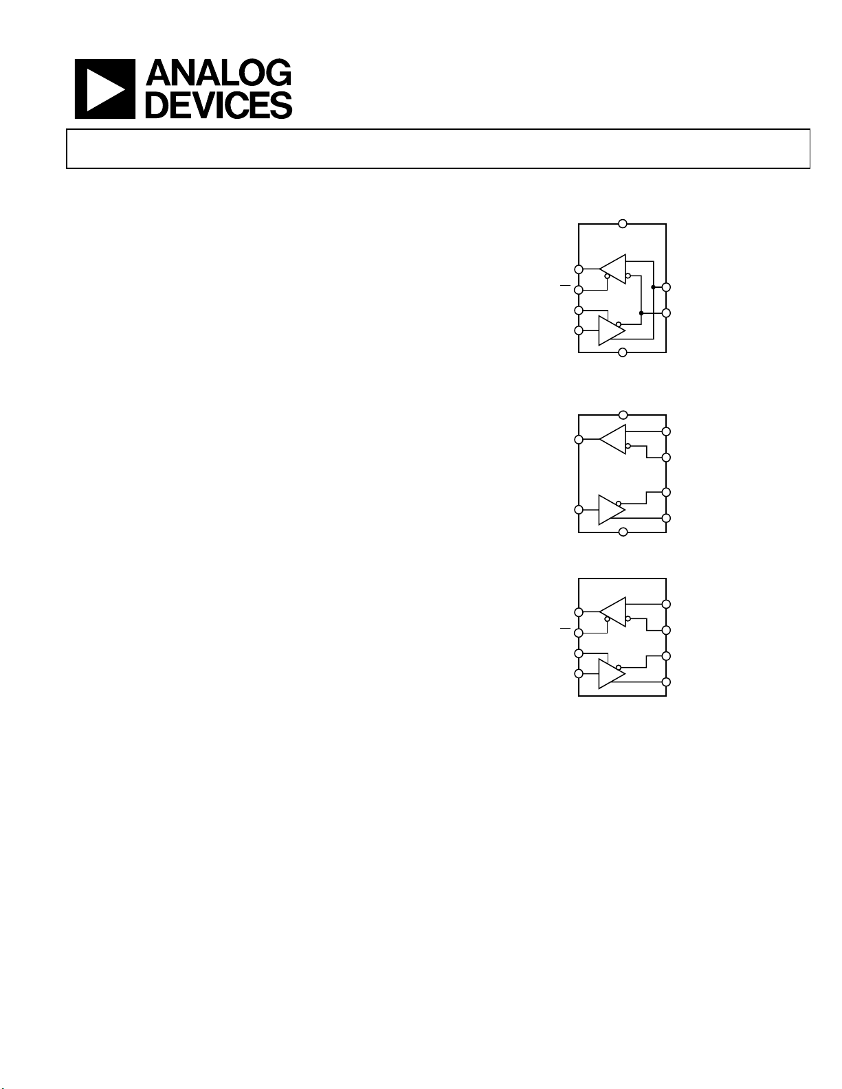
FUNCTIONAL BLOCK DIAGRAMS
CC
ADM3483/
ADM3485
RO
RE
DE
DI
RO
DI
RO
RE
DE
DI
in the internal driver circuitry during fault conditions, then the
thermal shutdown circuit forces the driver output into a high
impedance state. If the inputs are unconnected (floating), the
receiver contains a fail-safe feature that results in a logic high
output state. The parts are fully specified over the commercial
and industrial temperature ranges. The ADM3483/ADM3485/
ADM3488/ADM3490 are available in 8-lead SOIC_N; the
ADM3491 is available in a 14-lead SOIC_N.
R
D
GND
Figure 1.
CC
R
ADM3488/
ADM3490
D
GND
Figure 2.
ADM3491
R
D
Figure 3.
A
B
05524-027
A
B
Z
Y
05524-026
A
B
Z
Y
05524-025
Rev. B
Information furnished by Analog Devices is believed to be accurate and reliable. However, no
responsibility is assumed by Anal og Devices for its use, nor for any infringements of patents or ot her
rights of third parties that may result from its use. Specifications subject to change without notice. No
license is granted by implication or otherwise under any patent or patent rights of Analog Devices.
Trademarks and registered trademarks are the property of their respective owners.
One Technology Way, P.O. Box 9106, Norwood, MA 02062-9106, U.S.A.
Tel: 781.329.4700 www.analog.com
Fax: 781.461.3113 ©2006 Analog Devices, Inc. All rights reserved.

ADM3483/ADM3485/ADM3488/ADM3490/ADM3491
TABLE OF CONTENTS
Features.............................................................................................. 1
Applications....................................................................................... 1
General Description ......................................................................... 1
Functional Block Diagrams............................................................. 1
Revision History ............................................................................... 2
Specifications..................................................................................... 4
Timing Specifications—ADM3485/ADM3490/ADM3491.... 5
Timing Specifications—ADM3483/ADM3488........................ 5
Timing Specifications—ADM3483/ADM3485/ADM3488/
ADM3490/ADM3491.................................................................. 6
Absolute Maximum Ratings............................................................ 7
ESD Caution.................................................................................. 7
Pin Configurations and Function Descriptions ........................... 8
Test Circuits....................................................................................... 9
Switching Characteristics ..............................................................11
Typical Performance Characteristics........................................... 12
Circuit Description......................................................................... 14
Devices with Receiver/Driver Enables—
ADM3483/ADM3485/ADM3491............................................ 14
Devices Without Receiver/Driver Enables—
ADM3488/ADM3490................................................................ 14
Reduced EMI and Reflections—ADM3483/ADM3488 ....... 14
Low Power Shutdown Mode..................................................... 14
Driver Output Protection.......................................................... 14
Propagation Delay...................................................................... 14
Typical Applications................................................................... 14
Line Length vs. Data Rate ......................................................... 15
Outline Dimensions....................................................................... 17
Ordering Guide .......................................................................... 18
REVISION HISTORY
10/06—Rev. A to Rev. B
Updated Format..................................................................Universal
Added ADM3491................................................................Universal
Changes to Specifications Section.................................................. 4
Changes to Typical Applications Section .................................... 14
7/06—Rev. 0 to Rev. A
Changes to Applications.................................................................. 1
Changes to General Description .................................................... 1
Changes to Figure 19...................................................................... 10
Changes to Typical Applications Section .................................... 13
Changes to Figure 31 and Figure 32............................................. 14
Updated Outline Dimensions....................................................... 15
10/05—Revision 0: Initial Version
Rev. B | Page 2 of 20

ADM3483/ADM3485/ADM3488/ADM3490/ADM3491
Table 1. ADM34xx Part Comparison
Guaranteed Data
Part No.
ADM3483 0.25 3.0 to 3.6 Half Yes Yes 2 8
ADM3485 10 3.0 to 3.6 Half No Yes 2 8
ADM3488 0.25 3.0 to 3.6 Full Yes No N/A 8
ADM3490 10 3.0 to 3.6 Full No No N/A 8
ADM3491 10 3.0 to 3.6 Full No Yes 2 14
Rate (Mbps)
Supply
Voltage (V)
Half-/FullDuplex
Slew Rate
Limited
Driver/Receiver
Enable
Shutdown
Current (nA)
Pin
Count
Rev. B | Page 3 of 20
ADM3483/ADM3485/ADM3488/ADM3490/ADM3491
SPECIFICATIONS
VCC = 3.3 V ± 0.3 V, TA = T
Table 2.
Parameter Min Typ Max Unit Test Conditions/Comments
DRIVER
Differential Output Voltage (VOD) 2.0 V RL = 100 Ω (RS-422), VCC = 3.3 V ± 5% (see Figure 7)
1.5 V RL = 54 Ω (RS-485) (see Figure 7)
1.5 V RL = 60 Ω (RS-485), VCC = 3.3 V (see Figure 8)
∆ |VOD| for Complementary Output States
Common-Mode Output Voltage (VOC) 3 V RL = 54 Ω or 100 Ω (see Figure 7)
∆ |VOC| for Common-Mode Output Voltage
DRIVER INPUT LOGIC
CMOS Input Logic Threshold Low ( VIH) 0.8 V
CMOS Input Logic Threshold High (VIL) 2.0 V
CMOS Logic Input Current (I
Output Leakage—Y, Z (IO)
Output Leakage (Y, Z) in Shutdown Mode (IO)
RECEIVER
Differential Input Threshold Voltage (VTH) −0.2 +0.2 V −7 V < VCM < +12 V
Input Hysteresis (∆ VTH) 50 mV VCM = 0 V
CMOS Output Voltage High (VOH) VCC – 0.4 V I
CMOS Output Voltage Low (VOL) 0.4 V I
Three-State Output Leakage Current (I
Input Resistance (RIN) 12 kΩ −7 V < VCM < +12 V
POWER SUPPLY CURRENT
Supply Current (ICC)
Supply Current in Shutdown Mode (I
Receiver Short-Circuit Output Current (I
1
ΔVOD and ΔVOC are the changes in VOD and VOC, respectively, when DI input changes state.
to T
MIN
)
IN2
, unless otherwise noted.
MAX
1
0.2 V RL = 54 Ω or 100 Ω (see Figure 7)
1
0.2 V RL = 54 Ω or 100 Ω (see Figure 7)
DE, DI,
DE, DI,
) ±2 µA
IN1
DE, DI,
1.0 mA VIN = 12 V, DE = 0 V, VCC = 0 V or 3.6 V Input Current—A, B (I
−0.8 mA V
0.1 µA
= −7 V, DE = 0 V, VCC = 0 V or 3.6 V
IN
= 12 V, DE = 0 V, RE = 0 V, VCC = 0 V or 3.6 V,
V
IN
RE
RE
RE
ADM3491 only
−0.1 µA
VIN = −7 V, DE = 0 V, RE = 0 V, VCC = 0 V or 3.6 V,
ADM3491 only
0.01 µA
= 12 V, DE = 0 V, RE = VCC, VCC = 0 V or 3.6 V,
V
IN
ADM3491 only
−0.01 µA
VIN = −7 V, DE = 0 V, RE = VCC, VCC = 0 V or 3.6 V,
ADM3491 only
= −1.5 mA, VID = 200 mV (see Figure 9)
OUT
= 2.5 mA, VID = 200 mV (see Figure 9)
OUT
) ±1 µA VCC = 3.6 V, 0 V ≤ V
OZR
1.1 2.2 mA
0.95 1.9 mA
) 0.002 1 µA
SHDN
OSD
)
−250 mA V
250 mA V
) ±8 ±60 mA 0 V < VRO < VCC
OSR
DE = V
CC
DE = 0 V,
DE = 0 V,
= −7 V Driver Short-Circuit Output Current (I
OUT
= 12 V
OUT
, RE = 0 V or VCC, no load, DI = 0 V or VCC
RE = 0 V, no load, DI = 0 V or VCC
RE = VCC, DI = VCC or 0 V
OUT
≤ VCC
Rev. B | Page 4 of 20

ADM3483/ADM3485/ADM3488/ADM3490/ADM3491
TIMING SPECIFICATIONS—ADM3485/ADM3490/ADM3491
VCC = 3.3 V, TA = 25°C, unless otherwise noted.
Table 3.
Parameter Min Typ Max Unit Test Conditions/Comments
DRIVER
Differential Output Delay (tDD) 1 22 35 ns
Differential Output Transition Time (tTD) 3 8 25 ns
Propagation Delay, Low-to-High Level (t
Propagation Delay, High-to-Low Level (t
|t
– t
| Propagation Delay Skew1 (t
PLH
PHL
DRIVER OUTPUT ENABLE/DISABLE TIMES (ADM3485/
) 7 22 35 ns
PLH
) 7 22 35 ns
PHL
) 8 ns
PDS
ADM3491 ONLY)
Output Enable Time to Low Level (t
Output Enable Time to High Level (t
Output Disable Time from High Level (t
Output Disable Time from Low Level (t
Output Enable Time from Shutdown to Low Level (t
Output Enable Time from Shutdown to High Level (t
1
Measured on |t
PLH
(Y) − t
(Y)| and |t
PHL
PLH
) 45 90 ns
PZL
) 45 90 ns
PZH
) 40 80 ns
PHZ
) 40 80 ns
PLZ
) 650 900 ns
PSL
) 650 900 ns
PSH
(Z) − t
(Z)|.
PHL
RL = 60 Ω (see Figure 10 and Figure 16)
RL = 60 Ω (see Figure 10 and Figure 16)
RL = 27 Ω (see Figure 11 and Figure 17)
RL = 27 Ω (see Figure 11 and Figure 17)
RL = 27 Ω (see Figure 11 and Figure 17)
RL = 110 Ω (see Figure 13 and Figure 19)
RL = 110 Ω (see Figure 12 and Figure 18)
RL = 110 Ω (see Figure 12 and Figure 18)
RL = 110 Ω (see Figure 13 and Figure 19)
RL = 110 Ω (see Figure 13 and Figure 19)
RL = 110 Ω (see Figure 12 and Figure 18)
TIMING SPECIFICATIONS—ADM3483/ADM3488
VCC = 3.3 V, TA = 25°C, unless otherwise noted.
Table 4.
Parameter Min Typ Max Unit Test Conditions/Comments
DRIVER
Differential Output Delay (tDD) 600 900 1400 ns
Differential Output Transition Time (tTD) 400 700 1200 ns
Propagation Delay, Low-to-High Level (t
Propagation Delay, High-to-Low Level (t
|t
– t
| Propagation Delay Skew1 (t
PLH
PHL
) 700 1000 1500 ns
PLH
) 700 1000 1500 ns
PHL
) 100 ns
PDS
DRIVER OUTPUT ENABLE/DISABLE TIMES (ADM3483 ONLY)
Output Enable Time to Low Level (t
Output Enable Time to High Level (t
Output Disable Time from High Level (t
Output Disable Time from Low Level (t
Output Enable Time from Shutdown to Low Level (t
Output Enable Time from Shutdown to High Level (t
1
Measured on |t
PLH
(Y) − t
(Y)| and |t
PHL
PLH
) 900 1300 ns
PZL
) 600 800 ns
PZH
) 50 80 ns
PHZ
) 50 80 ns
PLZ
) 1.9 2.7 s
PSL
) 2.2 3.0 s
PSH
(Z) − t
(Z)|.
PHL
RL = 60 Ω (see Figure 10 and Figure 16)
RL = 60 Ω (see Figure 10 and Figure 16)
RL = 27 Ω (see Figure 11 and Figure 17)
RL = 27 Ω (see Figure 11 and Figure 17)
RL = 27 Ω (see Figure 11 and Figure 17)
= 110 Ω (see Figure 13 and Figure 19)
R
L
RL = 110 Ω (see Figure 12 and Figure 18)
RL = 110 Ω (see Figure 12 and Figure 18)
RL = 110 Ω (see Figure 13 and Figure 19)
RL = 110 Ω (see Figure 13 and Figure 19)
RL = 110 Ω (see Figure 12 and Figure 18)
Rev. B | Page 5 of 20
ADM3483/ADM3485/ADM3488/ADM3490/ADM3491
TIMING SPECIFICATIONS—ADM3483/ADM3485/ADM3488/ADM3490/ADM3491
VCC = 3.3 V, TA = 25°C, unless otherwise noted.
Table 5.
Parameter Min Typ Max Unit Test Conditions/Comments
RECEIVER
Time to Shutdown (t
ADM3483/ADM3485/ADM3491
Propagation Delay, Low-to-High Level (t
ADM3485/ADM3490/ADM3491 25 65 90 ns VID = 0 V to 3.0 V, CL = 15 pF (see Figure 14 and Figure 20)
ADM3483/ADM3488 25 75 120 ns
Propagation Delay, High-to-Low Level (t
ADM3485/ADM3490/ADM3491 25 65 90 ns VID = 0 V to 3.0 V, CL = 15 pF (see Figure 14 and Figure 20)
ADM3483/ADM3488 25 75 120 ns
|t
– t
| Propagation Delay Skew (t
PLH
PHL
ADM3485/ADM3490/ADM3491 10 ns VID = 0 V to 3.0 V, CL = 15 pF (see Figure 14 and Figure 20)
ADM3483/ADM3488 20 ns
RECEIVER OUTPUT ENABLE/DISABLE TIMES
(ADM3483/ADM3485/ADM3491 ONLY)
Output Enable Time to Low Level (t
Output Enable Time to High Level (t
Output Disable Time from High Level (t
Output Disable Time from Low Level (t
Output Enable Time from Shutdown to
Low Level (t
PRSL
)
Output Enable Time from Shutdown to
High Level (t
1
The transceivers are put into shutdown by bringing the RE high and DE low. If the inputs are in this state for less than 80 ns, the parts are guaranteed not to enter
shutdown. If the parts are in this state for 300 ns or more, the parts are guaranteed to enter shutdown.
PRSH
)
SHDN
)
1
RPLH
RPHL
RPDS
80 190 300 ns
)
)
)
) 25 50 ns CL = 15 pF (see Figure 15 and Figure 21)
PRZL
) 25 50 ns CL = 15 pF (see Figure 15 and Figure 21)
PRZH
) 25 45 ns CL = 15 pF (see Figure 15 and Figure 21)
PRHZ
) 25 45 ns CL = 15 pF (see Figure 15 and Figure 21)
PRLZ
720 1400 ns CL = 15 pF (see Figure 15 and Figure 21)
720 1400 ns C
= 15 pF (see Figure 15 and Figure 21)
L
Rev. B | Page 6 of 20

ADM3483/ADM3485/ADM3488/ADM3490/ADM3491
ABSOLUTE MAXIMUM RATINGS
TA = 25°C, unless otherwise noted.
Table 6.
Parameter Rating
VCC to GND 7 V
Digital I/O Voltage (DE, RE, DI)
Digital I/O Voltage (RO) VCC − 0.5 V to VCC + 0.5 V
Driver Output/Receiver Input Voltage −7.5 V to +12.5 V
Operating Temperature Range −40°C to +85°C
Storage Temperature Range −65°C to +125°C
θJA Thermal Impedance
8-Lead SOIC 121°C/W
14-Lead SOIC 86°C/W
Lead Temperature
Soldering (10 sec) 300°C
Vapor Phase (60 sec) 215°C
Infrared (15 sec) 220°C
−0.3 V to V
+ 0.3 V
CC
Stresses above those listed under Absolute Maximum Ratings
may cause permanent damage to the device. This is a stress
rating only; functional operation of the device at these or any
other conditions above those indicated in the operational
section of this specification is not implied. Exposure to absolute
maximum rating conditions for extended periods may affect
device reliability.
ESD CAUTION
Rev. B | Page 7 of 20

ADM3483/ADM3485/ADM3488/ADM3490/ADM3491
G
PIN CONFIGURATIONS AND FUNCTION DESCRIPTIONS
14
V
CC
13
V
CC
12
A
B
11
10
Z
Y
9
NC
8
RO
RE
DE
DI
1
ADM3483/
2
ADM3485
3
TOP VIEW
(Not to Scale)
4
NC
1
RO
2
8
V
CC
B
7
A
6
GND
5
05524-028
V
CC
RO 2
DI 3
ND 4
1
ADM3488/
ADM3490
TOP VIEW
(Not to Scale)
8
A
B7
Z6
Y5
05524-029
3
RE
DE
4
(Not to Scale)
5
DI
GND
6
GND
7
NC = NO CONNECT
ADM3491
TOP VIE W
Figure 4. ADM3483/ADM3485 Pin Configuration Figure 5. ADM3488/ADM3490 Pin Configuration Figure 6. ADM3491 Pin Configuration
Table 7. Pin Function Descriptions
ADM3483/ADM3485
Pin No.
1 2 2 RO
ADM3488/ADM3490
Pin No.
ADM3491
Pin No.
Mnemonic Description
Receiver Output. When enabled, if A > B by 200 mV, then
RO = high. If A < B by 200 mV, then RO = low.
2 N/A 3
RE Receiver Output Enable. A low level enables the receiver
output, RO. A high level places it in a high impedance
RE is high and DE is low, the device enters a low
state. If
power shutdown mode.
3 N/A 4 DE
Driver Output Enable. A high level enables the driver differential
Output A and Output B. A low level places it in a high impedance
RE is high and DE is low, the device enters a low power
state. If
shutdown mode.
4 3 5 DI
Driver Input. With a half-duplex part when the driver is enabled, a
logic low on DI forces A low and B high while a logic high on
DI forces A high and B low. With a full-duplex part when the
driver is enabled, a logic low on DI forces Y low and Z high
while a logic high on DI forces Y high and Z low.
5 4 6, 7 GND Ground.
N/A 5 9 Y Noninverting Driver Output.
N/A 6 10 Z Inverting Driver Output.
6 N/A N/A A
Noninverting Receiver Input A and Noninverting Driver
Output A.
N/A 8 12 A Noninverting Receiver Input A.
7 N/A N/A B Inverting Receiver Input B and Inverted Driver Output B.
N/A 7 11 B Inverting Receiver Input B.
8 1 13, 14 V
CC
Power Supply (3.3 V ± 0.3 V).
N/A N/A 1, 8 NC No Connect.
05524-030
Rev. B | Page 8 of 20

ADM3483/ADM3485/ADM3488/ADM3490/ADM3491
2
V
TEST CIRCUITS
C
A/Y
B/Z
RL/2
V
OD
V
RL/2
OC
05524-003
GENERATOR
1
PPR = 250kHz, 50% DUT Y CYCLE ,
CL INCLUDES PROBE AND S TRAY CAPACITANCE .
1
50
V
CC
D
L
CL=15pF
t
6.0n s, ZO=50.
R
RL=
60
2
OUT
05524-036
Figure 7. Differential Output Voltage
and Common-Mode Voltage Drivers
375
V
R
OD
D
V
CC
L
375
Figure 8. Differential Output Voltage Drivers
with Varying Common-Mode Voltage
R
V
ID
0
V
OL
I
OL
(+)
VCM=
–7V TO +12V
V
OH
Figure 10. Driver Differential Output Delay and Transition Times
OM
C
1.5V
RL=27
=15pF
L
OUT
2
05524-037
S1
D
GENERATOR
05524-004
1
PPR = 250kHz , 50% DUTY CYCLE,
2
CL INCLUDES PROBE AND S TRAY CAPACITANCE.
1
50
V
CC
V
OH+VOL
V
=
OM
2
t
6.0ns, ZO=50.
R
Figure 11. Driver Propagation Delays
0V OR 3V
GENERATOR
I
OH
(–)
5524-005
1
PPR = 250kHz, 50% DUT Y CYCLE,
2
CL INCLUDES PROBE AND STRAY CAPACI TANCE.
1
50
D
S1
2
C
= 50pF
L
V
OH+VOL
=
V
OM
2
t
6.0n s, ZO=50.
R
1.5V
OUT
RL= 110
05524-038
Figure 9. CMOS Output Voltage High and
Figure 12. Driver Enable and Disable Times (t
PZH
, t
, t
)
PSH
PHZ
CMOS Output Voltage Low Receivers
Rev. B | Page 9 of 20

ADM3483/ADM3485/ADM3488/ADM3490/ADM3491
V
2
0V OR 3V
GENERATOR
1
PPR = 250k Hz, 50% DUT Y CYCL E,
2
CL INCLUDES PROBE AND STRAY CAPACIT ANCE.
1
50
S1
D
2
C
=50pF
L
t
6.0ns, ZO=50.
R
Figure 13. Driver Enable and Disable Times (t
V
ID
R
t
6.0ns, ZO=50.
R
1.5V
1
50
0
GENERATOR
1
PPR = 250kHz, 50% DUTY CYCLE,
CL INCLUDES PROBE AND STRAY CAPACI TANCE.
Figure 14. Receiver Propagation Delays
OUT
VOM=
CC
, t
PZL
C
RL= 110
OUT
, t
PSL
PLZ
=15pF
L
V
CC
2
+1.5V
–1.5V
1
PPR = 250kHz, 50% DUT Y CYCLE,
2
05524-039
CL INCLUDES PROBE AND ST RAY CAPACITANCE.
)
S3
V
R
ID
C
L
GENERATOR
1
50
t
6.0ns, ZO=50.
R
Figure 15. Receiver Enable and Disable Times
1k
2
S1
S2
V
CC
05524-041
2
05524-040
Rev. B | Page 10 of 20

ADM3483/ADM3485/ADM3488/ADM3490/ADM3491
V
V
V
V
V
V
V
SWITCHING CHARACTERISTICS
+3
IN
OUT
1.5V 1.5V
t
DD
t
TD
0
t
DD
90%90%
50%50%
10%10%
+2V
–2V
t
TD
05524-006
Figure 16. Driver Differential Output Delay and Transition Times
3
IN
A/Y
OUT
B/Z
OUT
1.5V 1.5V
t
PLH
V
OM
t
PHL
V
OM
0V
t
PHL
V
PLH
OH
V
OL
V
OH
V
OL
05524-007
V
OM
t
V
OM
Figure 17. Driver Propagation Delays
1.5V1.5V
t
PHZ
V
OM
0.25V
OUT
IN
t
PZH
Figure 18. Driver Enable and Disable Times (t
IN
OUT
1.5V 1.5V
t
PSL
V
OM
t
PLZ
0.25V
Figure 19. Driver Enable and Disable Times (t
PZH
3
0
V
OH
0
05524-008
, t
, t
)
PSH
PHZ
3
0
V
CC
V
OL
05524-009
, t
, t
PZL
)
PSL
PLZ
OUT
OUT
IN
IN
+0.25V
1.5V
t
t
PRSH
t
PRZH
PRHZ
1.5V
1.5V1. 5V
V
OM
OUT
IN
t
RPLH
Figure 20. Receiver Propagation Delays
+3
S1 OPEN
0
V
0
+3V
0
V
0
OH
OH
S2 CLOSED
S3 = +1.5V
S1 OPEN
S2 CLOSED
S3 = +1.5V
OUT
OUT
1.5V
Figure 21. Receiver Enable and Disable Times
IN
IN
t
RPHL
V
OM
+0.25V
1.5V
3
0
V
CC
0
05524-010
+3
S1 CLOSED
0
V
V
+3V
0
V
V
CC
OL
CC
OL
S2 OPEN
S3 = –1.5V
S1 CLOSED
S2 OPEN
S3 = –1.5V
5524-011
t
PRLZ
t
PRZL
t
PRSL
1.5V
1.5V
Rev. B | Page 11 of 20

ADM3483/ADM3485/ADM3488/ADM3490/ADM3491
–
TYPICAL PERFORMANCE CHARACTERISTICS
30
0.8
25
20
15
10
OUTPUT CURRENT (mA)
5
0
03
0.5 1.0 1.5 2.0 2.5 3.0
OUTPUT V OLTAG E (V)
05524-012
.5
Figure 22. Output Current vs. Receiver Output Low Voltage
16
–14
–12
–10
–8
–6
OUTPUT CURRENT (mA)
–4
–2
0
03
0.5 1.0 1.5 2.0 2.5 3.0
OUTPUT V OLTAG E (V)
05524-013
.5
Figure 23. Output Current vs. Receiver Output High Voltage
3.30
3.25
3.20
3.15
3.10
OUTPUT VOLTAGE (V)
3.05
3.00
–40
–30 –20 –10 0 10 20 30 40 50 60 70 80
TEMPERATURE (°C)
Figure 24. Receiver Output High Voltage vs. Temperature, I
RO
05524-014
= 1.5 mA
0.7
0.6
0.5
0.4
0.3
OUTPUT VOLTAGE (V)
0.2
0.1
0
–40
–30 –20 –10 0 10 20 30 40 50 60 70 80
Figure 25. Receiver Output Low Voltage vs. Temperature, I
100
90
80
70
60
50
40
30
OUTPUT CURRENT (mA)
20
10
0
03.5
Figure 26. Driver Output Current vs. Differential Output Voltage
2.6
2.5
2.4
2.3
2.2
2.1
2.0
1.9
OUTPUT VOLTAGE (V)
1.8
1.7
1.6
–30 –20 –10 0 10 20 30 40 50 60 70 80
–40
Figure 27. Driver Differential Output Voltage vs. Temperature, R
TEMPERATURE (°C)
0.5 1.0 1.5 2.0 2. 5 3.0
OUTPUT V OLTAG E (V)
TEMPERATURE (°C)
= 2.5 mA
RO
L
05524-015
05524-016
05524-017
= 54 Ω
Rev. B | Page 12 of 20
ADM3483/ADM3485/ADM3488/ADM3490/ADM3491
–
140
120
100
80
60
40
OUTPUT CURRENT (mA)
20
0
01
246810
OUTPUT V OLTAG E (V)
05524-018
2
Figure 28. Output Current vs. Driver Output Low Voltage
125
–115
–105
–95
–85
–75
–65
–55
–45
–35
OUTPUT CURRENT (mA)
–25
–15
–5
–7 3
–6 –5 –4 –3 –2 –1 0 1 2
OUTPUT V OLTAG E (V)
05524-019
Figure 29. Output Current vs. Driver Output High Voltage
1.2
1.1
1.0
0.9
0.8
0.7
0.6
SUPPLY CURRENT (mA)
0.5
0.4
0.3
–30 –20 –10 0 10 20 30 40 50 60 70 80
–40
DE = RE = X*
DE = RE = GND
TEMPERATURE (°C)
Figure 30. Supply Current vs. Temperature
90
80
70
60
50
40
30
SHUTDOWN CURRENT (n A)
20
10
0
–30 –20 –10 0 10 20 30 40 50 60 70 80
–40
TEMPERATURE (°C)
Figure 31. Shutdown Current vs. Temperature
*X = DON’T CARE
05524-020
05524-021
Rev. B | Page 13 of 20

ADM3483/ADM3485/ADM3488/ADM3490/ADM3491
CIRCUIT DESCRIPTION
The ADM3483/ADM3485/ADM3488/ADM3490/ADM3491
are low power transceivers for RS-485 and RS-422 communications. The ADM3483/ADM3488 transmit and receive at data
rates up to 250 kbps; the ADM3485/ADM3490/ADM3491 transmit at up to 10 Mbps. The ADM3488/ADM3490/ADM3491 are
full-duplex transceivers, while the ADM3483/ADM3485 are halfduplex transceivers. Driver enable (DE) and receiver enable (
RE
)
pins are included on the ADM3483/ADM3485/ADM3491. When
disabled, the driver and receiver outputs are high impedance.
DEVICES WITH RECEIVER/DRIVER ENABLES—
ADM3483/ADM3485/ADM3491
Table 8. Transmitting Truth Table
Transmitting Input Transmitting Output
RE
X2 1 1 0 1 Normal
X2 1 0 1 0 Normal
0 0 X2 High-Z3 High-Z3 Normal
1 0 X2 High-Z3 High-Z3 Shutdown
1
A and B outputs are Z and Y respectively, for full-duplex part (ADM3491).
2
X = don’t care.
3
High-Z = high impedance.
DE DI B1 A
Table 9. Receiving Truth Table
Receiving Input Receiving Output
DE1 A – B RO
RE
0 0 ≥ +0.2 V 1 Normal
0 0 ≤ −0.2 V 0 Normal
0 0 Inputs Open 1 Normal
1 0 X2 High-Z3 Shutdown
1
DE is a don’t care; X for the full-duplex part (ADM3491).
2
X = don’t care.
3
High-Z = high impedance.
1
Mode
Mode
REDUCED EMI AND REFLECTIONS—
ADM3483/ADM3488
The ADM3483/ADM3488 are slew rate limited transceivers,
minimizing EMI and reducing reflections caused by improperly terminated cables.
LOW POWER SHUTDOWN MODE
(ADM3483/ADM3485/ADM3491)
A low power shutdown mode is initiated by bringing RE high
and DE low. The devices do not shut down unless both the driver
and receiver are disabled (high impedance). In shutdown mode,
the devices typically draw only 2 nA of supply current. For these
devices, the t
low power shutdown mode; the t
PSH
and t
enable times assume the part is in the
PSL
and t
PZH
enable times assume
PZL
the receiver or driver was disabled, but the part is not shut down.
DRIVER OUTPUT PROTECTION
Two methods are implemented to prevent excessive output
current and power dissipation caused by faults or by bus
contention. Current limit protection on the output stage
provides immediate protection against short circuits over
the whole common-mode voltage range (see the
Performance Characteristics
section). In addition, a ther-
Ty pi ca l
mal shutdown circuit forces the driver outputs into a high
impedance state if the die temperature rises excessively.
PROPAGATION DELAY
Skew time is the difference between the low-to-high and highto-low propagation delays. Small driver/receiver skew times help
maintain a symmetrical mark-space ratio (50% duty cycle).
− t
The receiver skew time (|t
PRLH
for ADM3483/ADM3488). The driver skew times are 8 ns for
ADM3485/ADM3490/ADM3491 and typically under 100 ns for
ADM3483/ADM3488.
|) is under 10 ns (20 ns
PRHL
DEVICES WITHOUT RECEIVER/DRIVER ENABLES—
ADM3488/ADM3490
Table 10. Transmitting Truth Table
Transmitting Input Transmitting Output
DI Z Y
1 0 1
0 1 0
TYPICAL APPLICATIONS
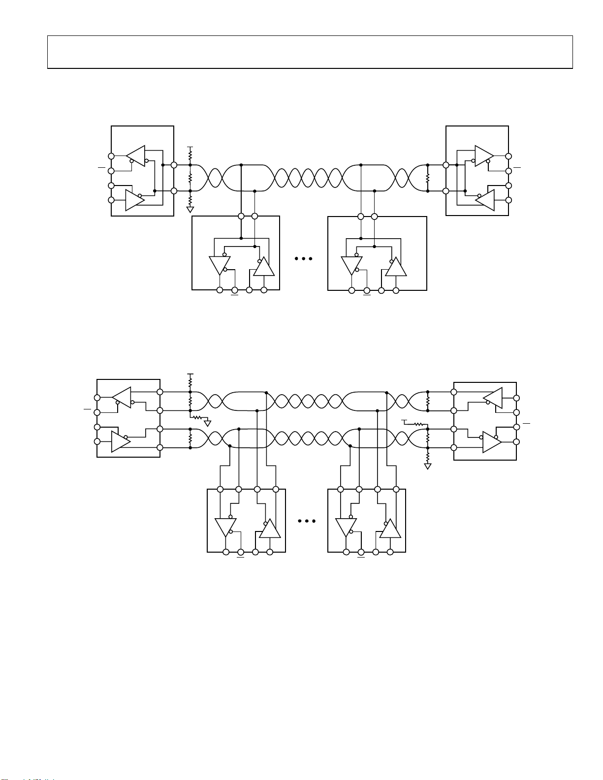
The ADM3483/ADM3485/ADM3491 transceivers are designed
for half-duplex bidirectional data communications on multipoint
bus transmission lines,
network applications circuits. The ADM3488 and the ADM3490
full-duplex transceivers are designed to be used in a daisy-chain
network topology or in a point-to-point application, see
and
To minimize reflections, the line must be terminated at both
Table 11. Receiving Truth Table
Receiving Input Receiving Output
A – B RO
≥ +0.2 V 1
≤ −0.2 V 0
Inputs open 1
Rev. B | Page 14 of 20
ends in its characteristic impedance, and stub lengths off the main
line must be kept as short as possible. The slew rate limited
ADM3483/ADM3488 are more tolerant of imperfect termination.
Figure 32 and Figure 33 show typical
Figure 34
Figure 35. The ADM3491 can be used as line repeat Figure 36.
ADM3483/ADM3485/ADM3488/ADM3490/ADM3491
A
X
LINE LENGTH VS. DATA RATE
The RS-485 and RS-422 standards cover line lengths up to 4000 feet. For line lengths greater than 4000 feet, see Figure 36.
MAXIMUM NUMBER OF T RANSCEIVERS ON BUS = 32
A
B
A
B
ADM3483/
ADM3485
R
A
T
B
ADM3483/
ADM3485
R
D
RO
RE
DE
DI
RO
RE
DE
DI
ADM3483/
ADM3485
R
D
V
CC
A
R
T
B
R1
R2
ADM3483/
ADM3485
R
RO
RE DI
NOTES
1. R
IS EQUAL T O THE CHARACTERISTIC IM PEDANCE OF THE CABLE.
T
Figure 32. ADM3483/ADM3485 Typical Half-Duplex RS-485 Network
V
CC
A
B
R1
R
T
R2
Z
R
T
Y
RO
RE
DE
MASTER
R
DI
D
ADM3491
A B Z Y
SLAVE
R
ADM3491
D
DE
M
IMUM NUMBER OF NO DES = 32
D
R
RE
RO
A B Z Y
R
D
DIDE
D
V
CC
SLAVE
ADM3491
05524-022
SLAVE
Y
R
T
Z
R1
B
R
T
A
R2
D
R
DI
DE
RE
RO
ADM3491
RO DIDE
RE
NOTES
1. R
IS EQUAL TO T HE CHARACTERISTIC IMPEDANCE OF THE CABLE.
T
RO DIDE
RE
05524-090
Figure 33. ADM3491 Typical Full-Duplex RS-485 Network
Rev. B | Page 15 of 20

ADM3483/ADM3485/ADM3488/ADM3490/ADM3491
RO
DI
MASTER
ADM3488/
ADM3490
R
D
A
B
Z
Y
ADM3488/
ADM3490
ABZY ABZY
ADM3488/
ADM3490
ADM3488/
ADM3490
Y
Z
B
A
SLAVE
R
D
DI
RO
SLAVE
RO
R
D
DI RO DI
R
SLAVE
D
Figure 34. ADM3488/ADM3490 Full-Duplex Daisy-Chain Network
RO
DI
MASTER
ADM3488/
ADM3490
R
D
A
B
Z
Y
Y
Z
B
A
SLAVE
ADM3488/
ADM3490
D
R
DI
RO
Figure 35. ADM3488/ADM3490 Full-Duplex Point-to-Point Applications
ADM3491
RO
RE
R
A
DATA IN
R
T
B
05524-042
5524-043
DE
DI
NOTES
1. R
T
D
IS EQUAL T O THE CHARACTERISTIC I MPEDANCE OF T HE CABLE.
Z
DATA OUT
R
T
Y
Figure 36. Line Repeater for ADM3491
Rev. B | Page 16 of 20
05524-091

ADM3483/ADM3485/ADM3488/ADM3490/ADM3491
OUTLINE DIMENSIONS
5.00 (0.1968)
4.80 (0.1890)
4.00 (0.1574)
3.80 (0.1497)
0.25 (0.0098)
0.10 (0.0040)
COPLANARITY
0.10
CONTROLLING DIMENSIONS ARE IN MILLIMETERS; INCH DIMENSIONS
(IN PARENTHESES) ARE ROUNDED-OFF MILLIMETER EQUIVALENTS FOR
REFERENCE ONLY AND ARE NOT APPROPRIATE FOR USE IN DESIGN.
85
1.27 (0.0500)
SEATING
PLANE
COMPLIANT TO JEDEC STANDARDS MS-012-AA
BSC
6.20 (0.2440)
5.80 (0.2284)
41
1.75 (0.0688)
1.35 (0.0532)
0.51 (0.0201)
0.31 (0.0122)
0.25 (0.0098)
0.17 (0.0067)
0.50 (0.0196)
0.25 (0.0099)
8°
1.27 (0.0500)
0°
0.40 (0.0157)
Figure 37. 8-Lead Standard Small Outline Package [SOIC_N]
Narrow Body
(R-8)
Dimensions shown in millimeters and (inches)
8.75 (0.3445)
8.55 (0.3366)
4.00 (0.1575)
3.80 (0.1496)
14
1
8
6.20 (0.2441)
7
5.80 (0.2283)
× 45°
1.27 (0.0500)
0.25 (0.0098)
0.10 (0.0039)
COPLANARITY
0.10
CONTROLLING DIMENSIONS ARE IN MILLIMETERS; INCH DIMENSIONS
(IN PARENTHESES) ARE ROUNDED-OFF MILLIMETER EQUIVALENTS FOR
REFERENCE ONLY AND ARE NOT APPROPRIATE FOR USE IN DESIGN.
BSC
0.51 (0.0201)
0.31 (0.0122)
COMPLIANT TO JEDEC STANDARDS MS-012-AB
1.75 (0.0689)
1.35 (0.0531)
SEATING
PLANE
0.25 (0.0098)
0.17 (0.0067)
0.50 (0.0197)
0.25 (0.0098)
8°
0°
1.27 (0.0500)
0.40 (0.0157)
× 45°
Figure 38. 14-Lead Narrow Body Small Outline [SOIC_N]
Narrow Body
(R-14)
Dimensions shown in millimeters and (inches)
Rev. B | Page 17 of 20

ADM3483/ADM3485/ADM3488/ADM3490/ADM3491
ORDERING GUIDE
Model Temperature Range Package Description Package Option Ordering Quantity
ADM3483ARZ
1
ADM3483ARZ–REEL7
ADM3485ARZ
1
ADM3485ARZ–REEL7
ADM3488ARZ
1
ADM3488ARZ–REEL7
ADM3490ARZ
1
ADM3490ARZ–REEL7
ADM3491AR −40°C to +85°C 14-Lead Narrow Body Small Outline (SOIC_N) R-14
ADM3491AR-REEL −40°C to +85°C 14-Lead Narrow Body Small Outline (SOIC_N) R-14 2,500
ADM3491AR-REEL7 −40°C to +85°C 14-Lead Narrow Body Small Outline (SOIC_N) R-14 1,000
ADM3491ARZ
1
ADM3491ARZ-REEL
ADM3491ARZ-REEL71−40°C to +85°C 14-Lead Narrow Body Small Outline (SOIC_N) R-14 1,000
1
Z = Pb-free part.
−40°C to +85°C
1
−40°C to +85°C
−40°C to +85°C
1
−40°C to +85°C
−40°C to +85°C
1
−40°C to +85°C
−40°C to +85°C
1
−40°C to +85°C
8-Lead Narrow Body Small Outline (SOIC_N) R-8
8-Lead Narrow Body Small Outline (SOIC_N) R-8 1,000
8-Lead Narrow Body Small Outline (SOIC_N) R-8
8-Lead Narrow Body Small Outline (SOIC_N) R-8 1,000
8-Lead Narrow Body Small Outline (SOIC_N) R-8
8-Lead Narrow Body Small Outline (SOIC_N) R-8 1,000
8-Lead Narrow Body Small Outline (SOIC_N) R-8
8-Lead Narrow Body Small Outline (SOIC_N) R-8 1,000
−40°C to +85°C 14-Lead Narrow Body Small Outline (SOIC_N) R-14
1
−40°C to +85°C 14-Lead Narrow Body Small Outline (SOIC_N) R-14 2,500
Rev. B | Page 18 of 20

ADM3483/ADM3485/ADM3488/ADM3490/ADM3491
NOTES
Rev. B | Page 19 of 20

ADM3483/ADM3485/ADM3488/ADM3490/ADM3491
NOTES
©2006 Analog Devices, Inc. All rights reserved. Trademarks and
registered trademarks are the property of their respective owners.
D05524-0-10/06(B)
Rev. B | Page 20 of 20
 Loading...