

15 kV ESD Protected, 2.7 V to 3.6 V Serial
www.BDTIC.com/ADI
ADM3307E/ADM3310E/ADM3311E/ADM3312E/ADM3315E1
FEATURES
Green Idle power-saving mode
Single 2.7 V to 3.6 V power supply
Operates with 3 V logic
0.1 μF to 1 μF charge pump capacitors
Low EMI
Low power shutdown: 20 nA
Full RS-232 compliance
460 kb/s data rate
One receiver active in shutdown
ADM3307E/ADM3311E/ADM3312E/ADM3315E)
(
Two receivers active in shutdown (ADM3310E)
ESD >15 kV IEC 1000-4-2 on RS-232 I/Os
ESD >15 kV IEC 1000-4-2 on CMOS and RS-232 I/Os
(ADM3307E)
APPLICATIONS
Mobile phone handsets/data cables
Laptop and notebook computers
Printers
Peripherals
Modems
PDAs/Hand-Held Devices/Palmtop Computers
C1
C4
0.1µF
V
CC
10µF
TANTALUM
0.1µF
CERAMIC
+
OUTPUTS
1
INTERNAL 400kΩ PULL-UP RESISTOR ON EACH CMOS INPUT.
2
INTERNAL 5kΩ PULL-DOWN RESISTOR ON EACH RS-232 INPUT.
CMOS
INPUTS
CMOS
C2
0.1µF
ENABLE
INPUT
1
R1
R2
R3
R4
R5
T1
IN
T2
IN
T3
IN
OUT
OUT
OUT
OUT
OUT
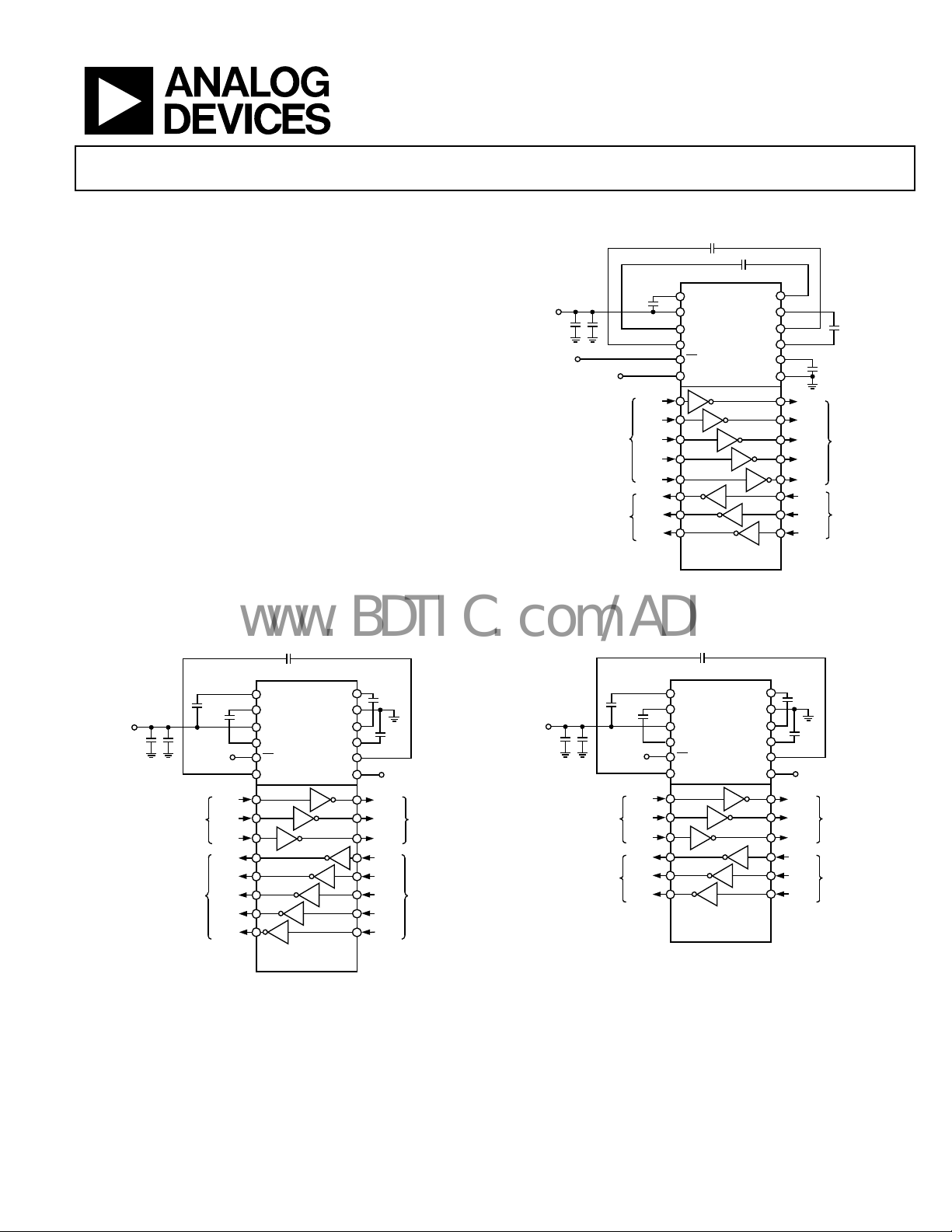
Figure 2. ADM3310E/ADM3311E Functional Block Diagram Figure 3. ADM3312E/ADM3315E Functional Block Diagram
0.1µF
VOLTAGE
V+
TRIPLER/
C2+
INVERTER
+3V TO ±9V
V
CC
C2–
EN
C1+
T2
T3
R4
R5
ADM3310E/
ADM3311E
C3
0.1µF
C3+
GND
C3–
V–
C5
C1–
T1
R2
R3
0.1µF
SHUTDOWN
SD
INPUT
T1
OUT
T2
OUT
T3
OUT
R1
R1
IN
R2
IN
R3
IN
R4
IN
R5
IN
Port Transceivers with Green Idle™
FUNCTIONAL BLOCK DIAGRAMS
C1
C2
0.1µF
0.1µF
EIA/TI A-232
OUTPUTS
EIA/TI A-232
2
INPUTS
V
CC
10µF
TANTALUM
ENABLE
INPUT
0.1µF
CERAMIC
+
SHUTDOWN
OUTPUTS
INPUT
CMOS
INPUTS
CMOS
0.1µF
1
C4
T1
IN
T2
IN
T3
IN
T4
IN
T5
IN
R1
OUT
R2
OUT
R3
OUT
V+
V
C2–
C1–
EN
SD
CC
T1
VOLTAGE
TRIPLER/
INVERTER
+3V TO ±9V
T2
ADM3307E
1
INTERNAL 400kΩ PULL-UP RE SISTO R ON EACH CMOS INPUT.
2
INTERNAL 5kΩ PULL-DOWN RESISTOR ON EACH RS-232 INPUT.
Figure 1. ADM3307E Functional Block Diagram
C1
C4
0.1µF
0.1µF
CERAMIC
V
CC
+
10µF
TANTALUM
OUTPUTS
1
INTERNAL 400kΩ PULL-UP RESISTOR ON EACH CMOS INPUT.
2
INTERNAL 5kΩ (22kΩ FOR ADM3315E) PULL-DOWN RESISTOR ON
EACH RS-232 INPUT.
02915-002
CMOS
INPUTS
CMOS
C2
0.1µF
ENABLE
INPUT
1
R1
R2
R3
T1
IN
T2
IN
T3
IN
OUT
OUT
OUT
0.1µF
VOLTAGE
V+
TRIPLER/
C2+
INVERTER
+3V TO ±9V
V
CC
C2–
EN
C1+
T2
T3
R3
ADM3312E/
ADM3315E
C2+
C3+
C1+
C3–
V–
GND
T3
T4
T5
R1
R2
R3
C3+
GND
C3–
V–
C1–
SD
T1
R1
R2
T1
OUT
T2
OUT
T3
OUT
T4
OUT
T5
OUT
R1
IN
R2
IN
R3
IN
C3
0.1µF
C5
0.1µF
SHUTDOWN
INPUT
T1
OUT
T2
OUT
T3
OUT
R1
IN
R2
IN
R3
IN
C5
0.1µF
C3
0.1µF
EIA/TIA-232
OUTPUTS
EIA/TIA-232
INPUTS
EIA/TI A-232
OUTPUTS
EIA/TI A-232
2
INPUTS
2
02915-001
02915-003
1
Protected by U.S. Patent No. 5,606,491.
Rev. H
Information furnished by Analog Devices is believed to be accurate and reliable. However, no
responsibility is assumed by Anal og Devices for its use, nor for any infringements of patents or ot her
rights of third parties that may result from its use. Specifications subject to change without notice. No
license is granted by implication or otherwise under any patent or patent rights of Analog Devices.
Trademarks and registered trademarks are the property of their respective owners.
One Technology Way, P.O. Box 9106, Norwood, MA 02062-9106, U.S.A.
Tel: 781.329.4700 www.analog.com
Fax: 781.461.3113 ©2006 Analog Devices, Inc. All rights reserved.

ADM3307E/ADM3310E/ADM3311E/ADM3312E/ADM3315E
www.BDTIC.com/ADI
TABLE OF CONTENTS
Features.............................................................................................. 1
Pin Configurations and Function Descriptions............................8
Applications....................................................................................... 1
Functional Block Diagrams............................................................. 1
Revision History ............................................................................... 2
General Description ......................................................................... 3
Specifications..................................................................................... 4
Absolute Maximum Ratings............................................................ 6
ESD Caution.................................................................................. 6
Product Selection Guide.................................................................. 7
REVISION HISTORY
1/06—Rev. G to Rev. H
Updated Formatting................................................................. Universal
Updated Outline Dimensions..............................................................18
Changes to Ordering Guide.................................................................20
4/04—REV. F to REV. G
C
hanges to Ordering Guide...................................................................5
Updated Outline Dimensions..............................................................15
8/02—Rev. E to REV. F
AD
M3307E (REV. 0), ADM3311E (REV. E), and ADM3312E
(REV. A) Data Sheets Merged into REV. G of ADM33xxE. Universal
ADM3310E (REV. PrA Now Prelims) and ADM3315E
(REV. PrA) Added .................................................................... Universal
Edits to Features.......................................................................................1
Edits to Applications ...............................................................................1
Edits to General Description .................................................................1
Edits to Functional Block Diagrams..................................................... 2
Edits to Specifications...............................................................................
Edits to Absolute Maximum Ratings.................................................... 4
ADM33xx Product Selection Guide Added ........................................5
Added ADM3307E, ADM3310E, ADM3312E, and
Typical Performance Characteristics........................................... 10
Circuit Description......................................................................... 13
Enable and Shutdown................................................................ 15
Layout and Supply Decoupling ................................................ 15
ESD/EFT Transient Protection Scheme .................................. 15
ESD Testing (IEC 1000-4-2) ..................................................... 16
Outline Dimensions....................................................................... 18
Ordering Guide .......................................................................... 20
ADM3315E Pin Configurations............................................................6
Edits to Pin Function Descriptions.......................................................7
Added ADM3307E, ADM3310E, ADM3312E, and
ADM3315E Truth Tables .......................................................................7
Edits to TPCs 1–14 ..................................................................................8
TPCs 15–18 Deleted..............................................................................10
Edits to Circuit Description Section ...................................................11
Edits to Charge Pump DC-to-DC Voltage Converter Section........11
Edits to How Does It Work Section ....................................................11
Edits to Green Idle vs. Shutdown Section ..........................................12
Edits to Doesn’t It Increase Supply Voltage Ripple? Section............12
Edits to What About Electromagnetic Compatibility? Section.......12
Edits to Transmitter (Driver) Section.................................................12
Edits to Receiver Section ......................................................................12
Edits to Enable and Shutdown Section...............................................12
Edits to High Baud Rate Section..........................................................13
Edits to ESD/EFT Transient Protection Scheme ...............................13
Added Figures 8a and 8b and Renumbered the Figures
that Followed..........................................................................................13
Edits to ESD Testing (IEC 1000-4-2) Section ....................................14
Edits to Figure 9.....................................................................................14
Deleted Table II and Table III and replaced them with Table V.....14
Added RU-24 Package Outline Updated CP-32, RS-28
and RU-28...............................................................................................15
Rev. H | Page 2 of 24

ADM3307E/ADM3310E/ADM3311E/ADM3312E/ADM3315E
www.BDTIC.com/ADI
GENERAL DESCRIPTION
The ADM33xxE line of driver/receiver products is designed to
fully meet the EIA-232 standard while operating with a single
2.7 V to 3.6 V power supply. The devices feature an on-board
charge pump dc-to-dc converter, eliminating the need for dual
power supplies. This dc-to-dc converter contains a voltage
tripler and a voltage inverter that internally generates positive
and negative supplies from the input 3 V power supply. The dcto-dc converter operates in Green Idle mode, whereby the
charge pump oscillator is gated on and off to maintain the
output voltage at ±7.25 V under varying load conditions. This
minimizes the power consumption and makes these products
ideal for battery-powered portable devices.
The ADM33xxE devices are suitable for operation in harsh
e
lectrical environments and contain ESD protection up to
±15 kV on their RS-232 lines (ADM3310E, ADM3311E,
ADM3312E, and ADM3315E). The ADM3307E contains ESD
protection up to ±15 kV on all I/O lines (CMOS, RS-232,
and SD).
A shutdown facility that reduces the power consumption to 66 nW
is als
o provided. While in shutdown, one receiver remains active
(two receivers active with ADM3310E), thereby allowing monitoring of peripheral devices. This feature allows the device to be shut
down until a peripheral device begins communication.
The active receiver can alert the processor, which can then take
he ADM33xxE device out of the shutdown mode.
t
The ADM3307E contains five drivers and three receivers and is
in
tended for mobile phone data lump cables and portable
computing applications.
The ADM3311E contains three drivers and five receivers and is
in
tended for serial port applications on notebook/laptop
computers.
The ADM3310E is a low current version of the ADM3311E.
his device also allows two receivers to be active in shutdown
T
mode.
EN
,
The ADM3315E is a low current version of the ADM3312E,
wi
th a 22 kΩ receiver input resistance that reduces the drive
requirements of the DTE. Its main applications are PDAs,
palmtop computers, and mobile phone data lump cables.
The ADM33xxE devices are fabricated using CMOS technology
f
or minimal power consumption. All parts feature a high level
of overvoltage protection and latch-up immunity.
All ADM33xxE devices are available in a 32-lead 5 mm × 5 mm
P_VQ and in a TSSOP (ADM3307E, ADM3310E, and
LFCS
ADM3311E in a 28-lead TSSOP; ADM3312E and ADM3315E
in a 24-lead TSSOP). The ADM3311E also comes in a 28-lead
SSOP.
The ADM33xxE devices are ruggedized RS-232 line
ivers/receivers that operate from a single supply of 2.7 V to
dr
3.6 V. Step-up voltage converters coupled with level shifting
transmitters and receivers allow RS-232 levels to be developed
while operating from a single supply. Features include low
power consumption, Green Idle operation, high transmission
rates, and compatibility with the EU directive on electromagnetic compatibility. This EM compatibility directive includes
protection against radiated and conducted interference,
including high levels of electrostatic discharge.
EN
All RS-232 (and CMOS, SD, and
outputs are protected against electrostatic discharges (up to
±15 kV). This ensures compliance with IEC 1000-4-2
requirements.
These devices are ideally suited for operation in electrically
ha
rsh environments or where RS-232 cables are frequently
being plugged/unplugged. They are also immune to high RF
field strengths without special shielding precautions.
Emissions are also controlled to within very strict limits. CMOS
te
chnology is used to keep the power dissipation to an absolute
minimum, allowing maximum battery life in portable
applications.
for ADM3307E) inputs and
The ADM3312E contains three drivers and three receivers and
tended for serial port applications, PDAs, mobile phone
is in
data lump cables, and other hand-held devices.
Rev. H | Page 3 of 24
ADM3307E/ADM3310E/ADM3311E/ADM3312E/ADM3315E
www.BDTIC.com/ADI
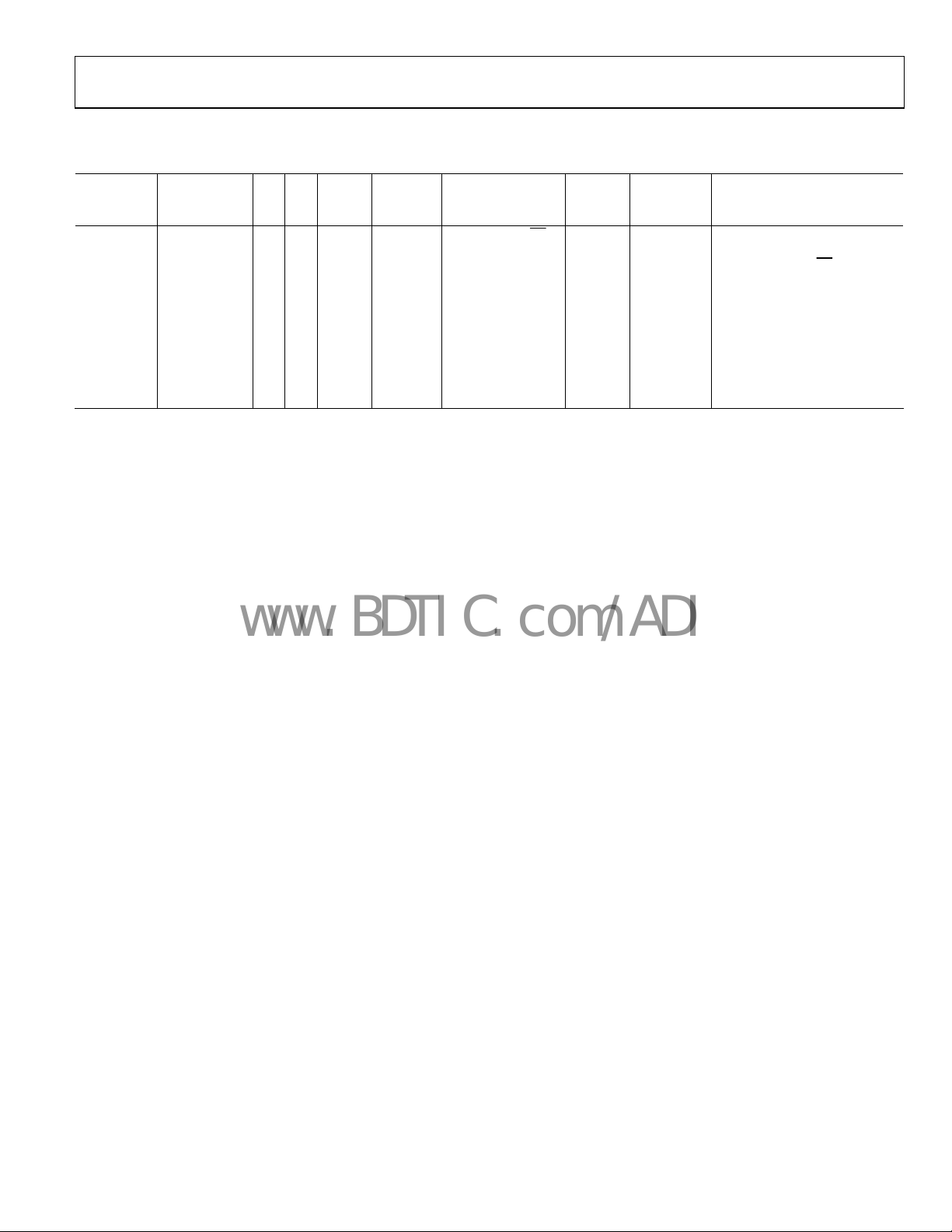
SPECIFICATIONS
VCC = 2.7 V to 3.6 V, C1 to C5 = 0.1 μF. All specifications T
Table 1
Parameter Min Typ Max Unit Test Conditions/Comments
Operating Voltage Range 2.7 3.3 3.6 V
VCC Power Supply Current
ADM3307E 0.75 1.5 mA VCC = 3.0 V to 3.6 V; no load
0.75 4.5 mA VCC = 2.7 V to 3.6 V; no load
ADM3311E, ADM3312E 0.45 1 mA No load; VCC = 3.0 V to 3.6 V; TA = 0°C to 85°C
0.45 4.5 mA No load; VCC = 2.7 V to 3.6 V; TA = − 40°C to +85°C
ADM3310E, ADM3315E 0.35 0.85 mA VCC = 2.7 V to 3.6 V; No load
ADM3310E, ADM3311E,
ADM3312E, ADM3315E
Shutdown Supply Current 0.02 1 μA
Input Pull-Up Current 10 25 μA TIN = GND
Input Leakage Current, SD,
Input Logic Threshold Low, V
0.4 V
Input Logic Threshold High, V
CMOS Output Voltage Low, VOL 0.4 V I
CMOS Output Voltage High, VOH V
CMOS Output Leakage Current
ADM3307E 0.04 ±1 μA
ADM3310E, ADM3311E 0.05 ±5 μA
ADM3312E, ADM3315E
Charge Pump Output Voltage, V+ +7.25 V No load
ADM3307E, ADM3311E, ADM3312E
Charge Pump Output Voltage, V− −7.25 V No load
ADM3307E, ADM3311E, ADM3312E
Charge Pump Output Voltage, V+ +6.5 V No load
ADM3310E, ADM3315E
Charge Pump Output Voltage, V− −6.5 V No load
ADM3310E, ADM3315E
EIA-232 Input Voltage Range −25 +25 V
EIA-232 Input Threshold Low 0.4 1.3 V
EIA-232 Input Threshold High 2.0 2.4 V
EIA-232 Input Hysteresis 0.14 V
EIA-232 Input Resistance
ADM3307E, ADM3310E, ADM3311E,
ADM3312E
ADM3315E 14 22 31 kΩ
Output Voltage Swing
ADM3310E, ADM3315E ±5.0 ±5.5 V All transmitter outputs loaded with 3 kΩ to ground
ADM3307E, ADM3311E, ADM3312E ±5.0 ±6.4 V VCC = 3.0 V
±5.5 V VCC = 2.7 V
All transmitter outputs loaded with 3 kΩ to ground
Transmitter Output Resistance 300 Ω VCC = 0 V, V
RS-232 Output Short-Circuit Current ±15 ±60 mA
EN
0.8 V
INL
2.0 V
INH
35 mA R
0.02 ±1 μA
− 0.6 V I
CC
3 5 7 kΩ
MIN
to T
, unless otherwise noted.
MAX
TIN, EN, SHDN
TIN, EN, SHDN; VCC = 2.7 V
TIN, EN, SHDN
OUT
OUT
EN
EN
= 3 kΩ to GND on all T
L
= 1.6 mA
= −200 μA
= VCC, 0 V < R
= VCC, 0 V < R
OUT
OUT
OUT
= ±2 V
< VCC
< VCC
OUTS
Rev. H | Page 4 of 24
ADM3307E/ADM3310E/ADM3311E/ADM3312E/ADM3315E
www.BDTIC.com/ADI
Parameter Min Typ Max Unit Test Conditions/Comments
Maximum Data Rate
ADM3307E 250 720 kbps RL = 3 kΩ to 7 kΩ, CL = 50 pF to 1000 pF, VCC = 2.7 V
460 920 kbps RL = 3 kΩ to 7 kΩ, CL = 50 pF to 1000 pF, VCC = 3.0 V
ADM3310E, ADM3311E, ADM3312E,
250 460 kbps R
ADM3315E
Receiver Propagation Delay, T
, T
0.3 μs CL = 150 pF
PHL
PLH
0.17 1 μs CL = 150 pF; ADM3307E only
Receiver Output Enable Time, tER 100 ns
Receiver Output Disable Time, tDR 300 ns
Transmitter Propagation Delay, T
, T
500 ns RL = 3 kΩ, CL = 1000 pF
PHL
PLH
Transition Region Slew Rate 3 18 V/μs RL = 3 kΩ, CL = 50 pF to 1000 pF
ESD PROTECTION (I/O PINS) ±15 kV Human body model
±15 kV IEC 1000-4-2 air discharge
±8 kV IEC 1000-4-2 contact discharge
1
Measured at +3 V to −3 V or −3 V to +3 V.
2
Includes CMOS I/O, SD, and EN for ADM3307E.
= 3 kΩ to 7 kΩ, CL = 50 pF to 1000 pF, VCC = 3.0 V
L
1
2
Rev. H | Page 5 of 24
ADM3307E/ADM3310E/ADM3311E/ADM3312E/ADM3315E
www.BDTIC.com/ADI
ABSOLUTE MAXIMUM RATINGS
TA = 25°C, unless otherwise noted.
Table 2
Parameter Rating
VCC −0.3 V to +4 V
V+ (VCC − 0.3 V) to +9 V
V− +0.3 V to −9 V
Input Voltages
TIN −0.3 V to +6 V
RIN ±30 V
Output Voltages
T
±15 V
OUT
R
−0.3 V to (VCC + 0.3 V)
OUT
Short-Circuit Duration
T
Continuous
OUT
Thermal Impedance, θJA
LFCSP_VQ (CP-32-2) 32.5°C/W
TSSOP (RU-28) 68.0°C/W
TSSOP (RU-24) 68.0°C/W
SSOP (RS-28) 76.0°C/W
Operating Temperature Range
Industrial (A Version) −40°C to +85°C
Storage Temperature Range −65°C to +150°C
Lead Temperature (Soldering, 10 sec) 300°C
ESD Rating (IEC 1000-4-2 Air)
(RS-232 I/Os)
ESD Rating (IEC 1000-4-2 Contact)
(RS-232 I/Os)
±15 kV
±8 kV
Stresses above those listed under Absolute Maximum Ratings
may cause permanent damage to the device. This is a stress
rating only; functional operation of the device at these or any
other conditions above those indicated in the operation sections
of this specification is not implied. Exposure to absolute
maximum rating conditions for extended periods may affect
reliability.
ESD CAUTION
ESD (electrostatic discharge) sensitive device. Electrostatic charges as high as 4000 V readily accumulate on
the human body and test equipment and can discharge without detection. Although this product features
proprietary ESD protection circuitry, permanent damage may occur on devices subjected to high energy
electrostatic discharges. Therefore, proper ESD precautions are recommended to avoid performance degradation or loss of functionality.
Rev. H | Page 6 of 24
ADM3307E/ADM3310E/ADM3311E/ADM3312E/ADM3315E
www.BDTIC.com/ADI
PRODUCT SELECTION GUIDE
Table 3. Product Selection Guide
I
Generic
ADM3307E 2.7 V to 3.6 V 5 3 1 1 Mbps
ADM3310E 2.7 V to 3.6 V 3 5 2 460 kbps RS-232 0.85 mA 1 μA 2 Rxs active in shutdown, Green
ADM3311E 2.7 V to 3.6 V 3 5 1 460 kbps RS-232 1 mA 1 μA
ADM3312E 2.7 V to 3.6 V 3 3 1 460 kbps RS-232 1 mA 1 μA
ADM3315E 2.7 V to 3.6 V 3 3 1 460 kbps RS-232 0.85 mA 1 μA 22 kΩ Rx I/P resistance, Green
1
ICC shutdown is 20 nA typically.
Supply
Voltage
Tx
Rx
No. Rx
Active
in SD
Speed
15 kV ESD
RS-232 CMOS,
and SD
I
CC
Max
1.5 mA 1 μA ±15 kV ESD protection, CMOS
EN
,
CC
Shutdown
1
Max
Additional Features
on RS-2
32, and CMOS I/Os
including SD and
Idle mode level 6 V, low power
ADM3311E
Idle mode level 6 V, low power
ADM3312E
EN
pins
Rev. H | Page 7 of 24
ADM3307E/ADM3310E/ADM3311E/ADM3312E/ADM3315E
T
T
www.BDTIC.com/ADI
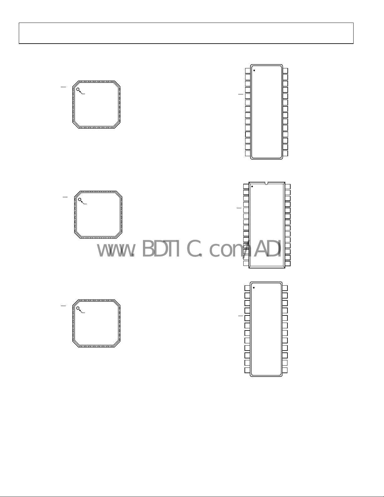
PIN CONFIGURATIONS AND FUNCTION DESCRIPTIONS
CC
C2+
C3+
V+
C1–
C2–
V
C1+
1EN
2SD
3NC
4
1
IN
5T2
IN
6T3
IN
7T4
IN
8T5
IN
26
29
28
27
31
30
32
PIN 1
INDICATOR
ADM3307E
TOP VIEW
(Not to Scale)
9
0
1
NC
OUT
R1
5
11
12
13
1
14
IN
NC
OUT
OUT
R2
R3
R2
R3
NC = NO CO NNECT
C3–
25
24 V–
23 GND
22 GND
21 T1
OUT
20 T2
OUT
19 T3
OUT
18 T4
OUT
17 T5
OUT
16
IN
IN
R1
2915-004
1
V+
2
V
CC
3
C2–
4
C1–
T1
T2
T3
T4
T5
R1
OUT
R2
OUT
R3
OUT
EN
SD
IN
IN
IN
IN
IN
ADM3307E
5
6
(Not to Scale)
7
8
9
10
11
12
13
14
TOP VIEW
Figure 4. ADM3307E LFCSP_VQ Pin Configuration Figure 5. SSOP/TSSOP Pin Configuration
CC
C3+
GND
C3–
V–
V+
V+
29
28
27
26
25
24 C1–
23 SD
22 NC
21 T1
OUT
20 T2
OUT
19 T3
OUT
18 R1
IN
17 R2
IN
12
15
13
14
16
IN
IN
IN
NC
NC
R4
R3
R5
2915-006
1
C2+
2
V
3
CC
4
C2–
ADM3310E/
EN
5
IN
IN
IN
ADM3311E
6
7
(Not to Scale)
8
9
10
11
12
13
14
TOP VIEW
C1+
T1
T2
T3
R1
OUT
R2
OUT
R3
OUT
R4
OUT
R5
OUT
OUT
OUT
1EN
2C1+
3NC
4T1
IN
5T2
IN
6T3
IN
7R1
8R2
C2+
C2–
V
30
31
32
PIN 1
INDICATOR
ADM3310E/
ADM3311E
TOP VIEW
(Not to Scale)
9
11
10
T
OUT
OU
OUT
R3
R5
R4
NC = NO CO NNECT
Figure 6. LFCSP_VQ Pin Configuration Figure 7. SSOP/TSSOP Pin Configuration
28
C2+
27
C3+
26
C1+
25
C3–
24
V–
23
GND
22
T1
OUT
21
T2
OUT
20
T3
OUT
19
T4
OUT
18
T5
OUT
17
R1
IN
16
R2
IN
15
R3
IN
02915-005
C3+
28
27
GND
C3–
26
V–
25
24
C1–
SD
23
T1
22
OUT
T2
21
OUT
20
T3
OUT
R1
19
IN
R2
18
IN
17
R3
IN
R4
16
IN
R5
15
IN
2915-007
1EN
2C1+
3NC
4
1
IN
5T2
IN
6T3
IN
7NC
8NC
CC
C3+
GND
C3–
C2+
C2–
V
V+
28
27
26
29
30
31
32
PIN 1
INDICATOR
ADM3312E/
ADM3315E
TOP VIEW
(Not to Scale)
9
11
12
15
13
14
10
IN
NC
NC
OUT
OUT
OUT
R2
R1
R3
R3
R2
NC = NO CO NNECT
V–
25
24 C1–
23 SD
22 NC
21 T1
OUT
20 T2
OUT
19 T3
OUT
18 NC
17 NC
16
IN
IN
R1
2915-008
1
V+
2
C2+
3
V
CC
4
C2
ADM3312E/
5
ADM3315E
EN
C1+
T1
T2
T3
R1
OUT
R2
OUT
R3
OUT
IN
IN
IN
10
12
6
(Not to Scale)
7
8
9
11
TOP VIE W
24
C3+
23
GND
22
C3–
21
V–
20
C1–
19
SD
18
T1
OUT
17
T2
OUT
16
T3
OUT
15
R1
IN
14
R2
IN
13
R3
IN
02915-009
Figure 8. LFCSP_VQ Pin Configuration Figure 9. SSOP/TSSOP Pin Configuration
Rev. H | Page 8 of 24

ADM3307E/ADM3310E/ADM3311E/ADM3312E/ADM3315E
www.BDTIC.com/ADI
Table 4. Pin Function Descriptions
Mnemonic Function
V
Power Supply Input 2.7 V to 3.6 V.
CC
V+
V−
GND Ground Pin. Must be connected to 0 V.
C1+, C1−
C2+, C2−
C3+, C3−
T
IN
T
Transmitter (Driver) Outputs. Typically ±5.5 V (±6.4 V for ADM3311E and ADM3312E).
OUT
R
IN
R
Receiver Outputs. These are TTL/CMOS levels.
OUT
EN
SD
For ADM3307E, R
NC No Connect.
Table 5. ADM3307E Truth Table
SD
EN
0 0 Normal Operation Enabled Enabled Enabled
0 1 Normal Operation Enabled Disabled Disabled
1 0 Shutdown Disabled Disabled Enabled
1 1 Shutdown Disabled Disabled Disabled
Table 7. ADM3311 Truth Table
SD
EN
0 0 Normal Operation Enabled Enabled Enabled
0 1
1 0 Shutdown Disabled Disabled Enabled
1 1 Shutdown Disabled Disabled Disabled
Internally Generated Positive Supply, 7.25 V (6.5 V Nominal for ADM3310E, ADM3315E). Capacitor C4 is connected between
and V+.
V
CC
Internally Generated Positive Supply, −7.25 V (−6.5 V Nominal f
or ADM3310E, ADM3315E). Capacitor C5 is connected between
GND and V−.
External Capacitor 1 is connected between these pins. A 0.1 μF capacitor is r
ecommended, but larger capacitors up to 1 μF
can be used.
External Capacitor 2 is connected between these pins. A 0.1 μF capacitor is r
ecommended, but larger capacitors up to 1 μF
can be used.
External Capacitor 3 is connected between these pins. A 0.1 μF capacitor is r
ecommended, but larger capacitors up to 1 μF
can be used.
Transmitter (Driver) Inputs. These inputs accept TTL/CMOS levels. An internal 400 kΩ pull-up resistor to VCC is connected on
each input.
Receiver Inputs. These inputs accept RS-232 signal levels. An internal 5 kΩ pull-down resistor (22 kΩ for ADM3315E) to GND is
connected on each of these inputs.
Receiver Enable. A high level three-states all the receiver outputs.
Shutdown Control. A high level disables the charge pump and reduces the quiescent current to less than 1 μA. All
ansmitters and most receivers are disabled. One receiver remains active in shutdown (two receivers are active in shutdown
tr
for the ADM3310E).
3 is active in shutdown.
OUT
For ADM3310E, R
For ADM3311E, R
For ADM3312E, R
For ADM3315E, R
4 and R
OUT
5 is active in shutdown.
OUT
3 is active in shutdown.
OUT
3 is active in shutdown.
OUT
5 are active in shutdown.
OUT
Table 6. ADM3310E Truth Table
Status T
1–5 R
OUT
1–2 R
OUT
OUT
3
SD
Status T
EN
1–3 R
OUT
1–3 R
OUT
0 0 Normal Operation Enabled Enabled Enabled
0 1
Receivers
Enabled Disabled Disabled
Disabled
1 0 Shutdown Disabled Disabled Enabled
1 1 Shutdown Disabled Disabled Disabled
Table 8. ADM3312E/ADM3315E Truth Table
Status T
1–3 R
OUT
1–4 R
OUT
OUT
5
SD
Status T
EN
1–3 R
OUT
1–2 R
OUT
0 0 Normal Operation Enabled Enabled Enabled
Receivers
Disabled
Enabled Disabled Disabled
0 1 Normal Operation Enabled Disabled Disabled
1 0 Shutdown Disabled Disabled Enabled
1 1 Shutdown Disabled Disabled Disabled
OUT
OUT
4–5
3
Rev. H | Page 9 of 24

ADM3307E/ADM3310E/ADM3311E/ADM3312E/ADM3315E
www.BDTIC.com/ADI
TYPICAL PERFORMANCE CHARACTERISTICS
9
T
HIGH
OUT
7
5
Figure 10. Charge Pump V+ Exiting Shutdown
Figure 11. Charge Pump V− Exiting Shutdown
9
7
5
3
1
–1
V+/V– (V)
–3
–5
–7
–9
0 5 10 15 20
Figure 12. Charge Pump V+/ V
V+
V–
LOAD CURRENT (mA)
− vs. Load Current (V
= 3.3 V)
CC
SD
SD
V–
3
V+
02915-010
02915-011
02915-012
1
Tx O/P (V)
–1
–3
–5
T
LOW
OUT
–7
0 200 400 600 800 1000
Figure 13. Transmitter Output v
40
35
30
25
20
15
SLEW RATE (V/µs)
10
5
0
0
LOAD CAPACIT ANCE (pF)
s. Load Capacitance
= 3.3 V, Data Rate = 460 kbps)
(V
CC
LOAD CAPACIT ANCE (pF)
Figure 14. Slew Rate vs. Load Capacitance (V
25
20
15
(mA)
CC
I
10
5
0
0 200 400 600 800 1000 1200
LOAD CAPACIT ANCE (pF)
Figure 15. Supply Current vs. Load Capacitance (R
= 3.3 V, Data Rate = 460 kbps)
(V
CC
= 3.3 V)
CC
= 3 kΩ)
L
02915-013
2500200015001000500
02915-014
02915-015
Rev. H | Page 10 of 24

ADM3307E/ADM3310E/ADM3311E/ADM3312E/ADM3315E
www.BDTIC.com/ADI
25
20
15
(mA)
CC
I
10
5
0
0 200 400 600 800 12001000
LOAD CAPACIT ANCE (pF)
Figure 16. Supply Current vs. Load Capacitance (R
= 3.3 V, Data Rate = 460 kbps)
(V
CC
30
28
26
24
22
20
18
16
SUPPLY CURRENT (mA)
14
12
10
0 200 400 600 800 1000
LOAD CAPACIT ANCE (pF)
Figure 17. Supply Current vs. Load Capacitance (V
460kbps
250kbps
125kbps
CC
= Infinite)
L
= 3.3 V, RL = 5 kΩ)
SD
TX O/P LOW
02915-016
02915-019
Figure 19. Transmitter Output (Low) Exiting Shutdown
10
8
6
4
2
0
VOLTAGE (V)
–2
OUT
Tx
–4
–6
–8
–10
0 200 400 600 800 1000
2915-017
Figure 20. Transmitter Output Voltag
= 3.3 V, CLK = 1 Mb/s, RL = 5 kΩ, ADM3307E)
(V
CC
300
LOAD CAPACIT ANCE (pF)
e High/Low vs. Load Capacitance
02915-020
SD
TX O/P
HIGH
02915-018
Figure 18. Transmitter Output (High) Exiting Shutdown
Rev. H | Page 11 of 24
250
200
150
100
OSCILLAT OR FREQUENCY (kHz)
50
0
0 5 10 15 20
Figure 21. Oscillator Freque
LOAD CURRENT (mA)
ncy vs. Load Current
2915-021

ADM3307E/ADM3310E/ADM3311E/ADM3312E/ADM3315E
www.BDTIC.com/ADI
600
500
400
(µA)
300
CC
I
200
100
0
2.62.83.03.23.43.6
Figure 22. I
(V)
V
CC
vs. VCC (Unloaded)
CC
2915-022
25
20
15
(mA)
CC
I
10
5
0
2.6 2.8 3.0 3. 2 3.4 3.6
Figure 23. I
VCC(V)
vs. VCC (RL = 3 kΩ)
CC
02915-023
Rev. H | Page 12 of 24

ADM3307E/ADM3310E/ADM3311E/ADM3312E/ADM3315E
www.BDTIC.com/ADI
CIRCUIT DESCRIPTION
The internal circuitry consists mainly of four sections. These
include the following:
charge pump voltage converter
• A
• 3.3 V log
• EI
• T
Charge Pump DC-to-DC Voltage Converter
The charge pump voltage converter consists of a 250 kHz (300 kHz
for ADM3307E) oscillator and a switching matrix. The converter
generates a ±9 V supply from the input 3.0 V level. This is done in
two stages using a switched capacitor technique. First, the 3.0 V
input supply is tripled to 9.0 V using Capacitor C4 as the charge
storage element. The +9.0 V level is then inverted to generate −9.0
V using C5 as the storage element.
However, it should be noted that, unlike other charge pump dc-
o-dc converters, the charge pump on the ADM3307E does not
t
run open-loop. The output voltage is regulated to ±7.25 V (or
±6.5 V for the ADM3310E and ADM3315E) by the Green Idle
circuit and never reaches ±9 V in practice. This saves power as
well as maintains a more constant output voltage.
GND
INTERNAL
OSCILLATOR
The tripler operates in two phases. During the oscillator low
phase, S1 and S2 are closed and C1 charges rapidly to V
S4, and S5 are open, and S6 and S7 are closed.
During the oscillator high phase, S1 and S2 are open, and S3
nd S4 are closed, so the voltage at the output of S3 is 2V
a
voltage is used to charge C2. In the absence of any discharge
current, C2 charges up to 2V
oscillator high phase, as previously mentioned, S6 and S7 are
closed, so the voltage at the output of S6 is 3V
then used to charge C3. The voltage inverter is illustrated in
Figure 25.
ic to EIA-232 transmitters
A-232 to 3.3 V logic receivers
ransient protection circuit on all I/O lines
V
CC
VOLTAGE
TRIPLER
S1
S2
Figure 24. Charge Pump Voltage Tripler
V
CC
FROM
GND
S3
+
C1
S4
V
CC
after several cycles. During the
CC
S8
+
C3
S9
S5
S10
S11
+ +
C2
C5
S6
S7
+
V+ = 3V
C4
. This voltage is
CC
GND
V– = –(V+)
CC
CC
V
CC
. S3,
. This
CC
02915-024
During the oscillator high phase, S10 and S11 are open, while
S8 and S9 are closed. C3 is charged to 3V
from the output of
CC
the voltage tripler over several cycles. During the oscillator low
phase, S8 and S9 are open, while S10 and S11 are closed. C3 is
connected across C5, whose positive terminal is grounded and
whose negative terminal is the V− output. Over several cycles,
C5 charges to −3 V
.
CC
The V+ and V− supplies may also be used to power external
cir
cuitry if the current requirements are small. See Figure 12 in
e Typical Performance Characteristics section.
th
What Is Green Idle?
Green Idle is a method of minimizing power consumption
under idle (no transmit) conditions while still maintaining the
ability to transmit data instantly.
How Does it Work?
Charge pump type dc-to-dc converters used in RS-232 line
drivers normally operate open-loop, that is, the output voltage
is not regulated in any way. Under light load conditions, the
output voltage is close to twice the supply voltage for a doubler
and three times the supply voltage for a tripler, with very little
ripple. As the load current increases, the output voltage falls and
the ripple voltage increases.
Even under no-load conditions, the oscillator and charge pump
perate at a very high frequency with consequent switching
o
losses and current drain.
Green Idle works by monitoring the output voltage and
1
ma
intaining it at a constant value of around 7 V
voltage rises above 7.25 V
voltage falls below 7 V
2
the oscillator is turned off. When the
1
, the oscillator is turned on and a burst of
. When the
charging pulses is sent to the reservoir capacitor. When the
oscillator is turned off, the power consumption of the charge
pump is virtually zero, so the average current drain under light
load conditions is greatly reduced.
1
For ADM3310E and ADM3315E, replace with 6.5 V.
2
For ADM3310E and ADM3315E, replace with 6.25 V.
INTERNAL
OSCILLATOR
Figure 25. Charge Pump Voltage Inverter
02915-025
Rev. H | Page 13 of 24

ADM3307E/ADM3310E/ADM3311E/ADM3312E/ADM3315E
V
www.BDTIC.com/ADI
A block diagram of the Green Idle circuit is shown in Figure 26.
Both V+ and V− are monitored and compared to a reference
voltage derived from an on-chip band gap device. If either V+
or V− fall below 7 V
rises above 7.25 V
SHUTDOWN
1
, the oscillator starts up until the voltage
2
.
V+ VOLTAGE
COMPARATOR
WITH 250mV
HYSTERESIS
START/ST OP
START/ST OP
V– VOLTAGE
COMPARAT OR
WITH 250mV
HYSTERESIS
CHARGE
PUMP
V+
V–
BAND GAP
VOLTAGE
REFERENCE
TRANSCEIVERS
Figure 26. Block Diagram of Green Idle Circuit
02915-026
The operation of Green Idle for V+ under various load
conditions is illustrated in Figure 27. Under light load
nditions, C1 is maintained in a charged condition, and only a
co
single oscillator pulse is required to charge up C2. Under these
conditions, V+ may actually overshoot 7.25 V
O
1
7.25V
V+
2
7V
OSC
1
7.25V
V+
2
7V
OSC
1
7.25V
V+
2
7V
OSC
1
FOR ADM3310E AND ADM 3315E REPLACE W ITH 6.5V .
2
FOR ADM3310E AND ADM 3315E REPLACE W ITH 6.25V .
Figure 27. Operation of Green Idle under Various Load Conditions
ERSHOOT
LIGHT
LOAD
MEDIUM
LOAD
HEAVY
LOAD
2
slightly.
02915-027
Under medium load conditions, it may take several cycles for
2
C2 to charge up to 7.25 V
. The average frequency of the
oscillator is higher because there are more pulses in each burst
and the bursts of pulses are closer together and more frequent.
Under high load conditions, the oscillator is on continuously if
th
e charge pump output cannot reach 7.25 V
2
.
Green Idle Vs. Shutdown
Shutdown mode minimizes power consumption by shutting
down the charge pump altogether. In this mode, the switches in
the voltage tripler are configured so V+ is connected directly to
V
. V− is zero because there is no charge pump operation to
CC
charge C5. This means there is a delay when coming out of
shutdown mode before V+ and V− achieve their normal
operating voltages. Green Idle maintains the transmitter supply
voltages under transmitter idle conditions so this delay does not
occur.
Doesn’t Green Idle Increase Supply Voltage Ripple?
The ripple on the output voltage of a charge pump operating in
open-loop depends on three factors: the oscillator frequency,
the value of the reservoir capacitor, and the load current. The
value of the reservoir capacitor is fixed. Increasing the oscillator
frequency decreases the ripple voltage; decreasing the oscillator
frequency increases it. Increasing the load current increases the
ripple voltage; decreasing the load current decreases it. The
ripple voltage at light loads is naturally lower than that for high
load currents.
Using Green Idle, the ripple voltage is determined by the high
nd low thresholds of the Green Idle circuit. These are
a
nominally 7 V
1
and 7.25 V2, so the ripple is 250 mV under most
load conditions. With very light load conditions, there may be
some overshoot above 7.25 V
2
, so the ripple is slightly greater.
Under heavy load conditions where the output never reaches
2
7.25 V
, the Green Idle circuit is inoperative and the ripple
voltage is determined by the load current, the same as in a
normal charge pump.
What about Electromagnetic Compatibility?
Green Idle does not operate with a constant oscillator
frequency. As a result, the frequency and spectrum of the
oscillator signal vary with load. Any radiated and conducted
emissions also vary accordingly. Like other Analog Devices
RS-232 transceiver products, the ADM33xxE devices feature
slew rate limiting and other techniques to minimize radiated
and conducted emissions.
Rev. H | Page 14 of 24
1
For ADM3310E and ADM3315E, replace with 6.5 V.
2
For ADM3310E and ADM3315E, replace with 6.25 V.

ADM3307E/ADM3310E/ADM3311E/ADM3312E/ADM3315E
V
V
www.BDTIC.com/ADI
Transmitter (Driver) Section
The drivers convert 3.3 V logic input levels into EIA-232 output
levels. With V
= 3.0 V and driving an EIA-232 load, the
CC
output voltage swing is typically ±6.4 V (or ±5.5 V for
ADM3310E and ADM3315E).
Unused inputs may be left unconnected, because an internal
400 kV p
ull-up resistor pulls them high forcing the outputs into
a low state. The input pull-up resistors typically source 8 mA
when grounded, so unused inputs should either be connected to
V
or left unconnected in order to minimize power
CC
consumption.
Receiver Section
The receivers are inverting level shifters that accept RS-232
input levels and translate them into 3.3 V logic output levels.
The inputs have internal 5 kΩ pull-down resistors (22 kΩ for
the ADM3310E) to ground and are also protected against
overvoltages of up to ±30 V. Unconnected inputs are pulled to
0 V by the internal 5 kΩ (or 22 kΩ for the ADM3315E) pulldown resistor. This, therefore, results in a Logic 1 output level
for unconnected inputs or for inputs connected to GND.
The receivers have Schmitt trigger inputs with a hysteresis level
of
0.14 V. This ensures error-free reception for both noisy
inputs and for inputs with slow transition times.
ENABLE AND SHUTDOWN
The enable function is intended to facilitate data bus
connections where it is desirable to three-state the receiver
outputs. In the disabled mode, all receiver outputs are placed in
a high impedance state. The shutdown function is intended to
shut the device down, thereby minimizing the quiescent
current. In shutdown, all transmitters are disabled. All receivers
are shut down, except for Receiver R3 (ADM3307E,
ADM3312E, and ADM3315E), Receiver R5 (ADM3311E), and
Receiver R4 and Receiver R5 (ADM3310E). Note that disabled
transmitters are not three-stated in shutdown, so it is not
permitted to connect multiple (RS-232) driver outputs together.
The shutdown feature is very useful in battery-operated systems
use it reduces the power consumption to 66 nW. During
beca
shutdown, the charge pump is also disabled. When exiting
shutdown, the charge pump is restarted and it takes
approximately 100 μs for it to reach its steady-state operating
conditions.
3
EN INPUT
0V
V
RECEIVER
OUTPUT
V
OH
OL
t
DR
VOH–0.1V
+0.1V
V
OL
Figure 28. Receiver Disable Timing
2915-028
3
EN INPUT
0V
V
RECEIVER
OUTPUT
V
OH
OL
Figure 29. Receiver Enable Timing
t
ER
3V
0.4V
02915-029
High Baud Rate
The ADM33xxE features high slew rates, permitting data
transmission at rates well in excess of the EIA/RS-232E
specifications. RS-232 voltage levels are maintained at data rates
up to 230 kbps (460 kbps for ADM3307E) under worst-case
loading conditions. This allows for high speed data links
between two terminals.
LAYOUT AND SUPPLY DECOUPLING
Because of the high frequencies at which the ADM33xxE
oscillator operates, particular care should be taken with printed
circuit board layout, with all traces being as short as possible
and C1 to C3 being connected as close to the device as possible.
The use of a ground plane under and around the device is also
highly recommended.
When the oscillator starts up during Green Idle operation, large
c
urrent pulses are taken from V
. For this reason, VCC should
CC
be decoupled with a parallel combination of 10 μF tantalum and
0.1 μF ceramic capacitors, mounted as close to the V
pin as
CC
possible.
Capacitor C1 to Capacitor C3 can have values between 0.1 μF and 1
. Larger values give lower ripple. These capacitors can be either
μF
electrolytic capacitors chosen for low equivalent series resistance
(ESR) or nonpolarized types, but the use of ceramic types is highly
recommended. If polarized electrolytic capacitors are used, polarity
must be observed (as shown by C1+).
ESD/EFT TRANSIENT PROTECTION SCHEME
The ADM33xxE uses protective clamping structures on all inputs
and outputs that clamp the voltage to a safe level and dissipate the
energy present in ESD (electrostatic) and EFT (electrical fast
transients) discharges. A simplified schematic of the protection
structure is shown in
Figure 33 for ADM3307E protection structure).
Each input and output contains two back-to-back high speed
cl
amping diodes. During normal operation with maximum RS-232
signal levels, the diodes have no effect as one or the other is reverse
biased depending on the polarity of the signal. If, however, the
voltage exceeds about ±50 V, reverse breakdown occurs and the
voltage is clamped at this level. The diodes are large p-n junctions
designed to handle the instantaneous current surge that can exceed
several amperes.
Figure 30 and Figure 31 (see Figure 32 and
Rev. H | Page 15 of 24

ADM3307E/ADM3310E/ADM3311E/ADM3312E/ADM3315E
www.BDTIC.com/ADI
The transmitter outputs and receiver inputs have a similar
protection structure. The receiver inputs can also dissipate some
of the energy through the internal 5 kΩ (or 22 kΩ for the
ADM3310E) resistor to GND as well as through the protection
diodes.
RECEIVER
INPUT
R
IN
Figure 30. Receiver Input Protection Scheme
Rx
D1
D2
02915-030
ESD TESTING (IEC 1000-4-2)
IEC 1000-4-2 (previously 801-2) specifies compliance testing
using two coupling methods, contact discharge and air-gap
discharge. Contact discharge calls for a direct connection to the
unit being tested. Airgap discharge uses a higher test voltage but
does not make direct contact with the unit under testing. With
air discharge, the discharge gun is moved toward the unit under
testing, which develops an arc across the air gap, thus the term
air discharge. This method is influenced by humidity,
temperature, barometric pressure, distance, and rate of closure
of the discharge gun. The contact discharge method, while less
realistic, is more repeatable and is gaining acceptance in
preference to the air-gap method.
Tx
D1
D2
Figure 31. Transmitter Output Protection Scheme
TRANSMITT ER
OUTPUT
02915-031
The ADM3307E protection scheme is slightly different (see
Figure 32 and Figure 33). The receiver inputs, transmitter
i
nputs, and transmitter outputs contain two back-to-back high
speed clamping diodes. The receiver outputs (CMOS outputs),
the SD and
EN
pins, contain a single reverse biased high speed
clamping diode. Under normal operation with maximum
CMOS signal levels, the receiver output, SD, and
EN
protection
diodes have no effect because they are reversed biased. If,
however, the voltage exceeds about 15 V, reverse breakdown
occurs and the voltage is clamped at this level. If the voltage
reaches −0.7 V, the diode is forward biased and the voltage is
clamped at this level. The receiver inputs can also dissipate
some of the energy through the internal 5 kΩ resistor to GND
as well as through the protection diodes.
RECEIVE R
INPUT
R
IN
Figure 32. ADM3307E Receiver Input Protection Scheme
TRANSMIT TER
OUTPUT
Figure 33. ADM3307E Transmitter Output Protection Scheme
D3
D4
Rx
D1
D2
Tx
D3
D1
D2
RECEIVER
OUTPUT
TRANSMITTER
INPUT
Although very little energy is contained within an ESD pulse,
he extremely fast rise time coupled with high voltages can
t
cause failures in unprotected semiconductors. Catastrophic
destruction can occur immediately as a result of arcing or
heating. Even if catastrophic failure does not occur immediately,
the device can suffer from parametric degradation that can
result in degraded performance. The cumulative effects of
continuous exposure can eventually lead to complete failure.
I/O lines are particularly vulnerable to ESD damage. Simply
tou
ching or plugging in an I/O cable can result in a static
discharge that can damage or completely destroy the interface
product connected to the I/O port. Traditional ESD test
methods, such as the MIL-STD-883B method 3015.7, do not
fully test a product’s susceptibility to this type of discharge. This
test was intended to test a product’s susceptibility to ESD
damage during handling.
Each pin is tested with respect to all other pins. There are some
im
portant differences between the traditional test and the IEC
test.
• The IEC t
est is much more stringent in terms of discharge
energy. The peak current injected is over four times greater.
• The c
• The IEC t
02915-032
urrent rise time is significantly faster in the IEC test.
est is carried out while power is applied to the
device.
It is possible that the ESD discharge could induce latch-up in
he device under test. This test, therefore, is more representative
t
of a real world I/O discharge where the equipment is operating
normally with power applied. For maximum peace of mind,
however, both tests should be performed, ensuring maximum
02915-033
protection both during handling and later during field service.
The protection structures achieve ESD protection up to ±15 kV
on all RS-232 I/O lines (and all CMOS lines, including SD and
EN
for the ADM3307E). For methods used to test the
protection scheme, see the ESD Testing (IEC 1000-4-2) section.
Rev. H | Page 16 of 24

ADM3307E/ADM3310E/ADM3311E/ADM3312E/ADM3315E
www.BDTIC.com/ADI
HIGH
VOLTAGE
GENERATOR
R1
C1
ESD TEST METHOD R2 C1
HUMAN BODY MO DEL
ESD ASSOC. STD 55.1
IEC1000-4-2
R2
1.5kV 100pF
330V 15 0pF
Figure 34. ESD Test Standards
100
90
(%)
PEAK
I
36.8
10
t
RL
t
DL
Figure 35. Human Body Model ESD Current Waveform
100
90
DEVICE
UNDER TEST
TIME
t
The ADM33xxE devices are tested using both of the previously
mentioned test methods. All pins are tested with respect to all
other pins as per the Human Body Model, ESD Assoc. Std. 55.1
specification. In addition, all I/O pins are tested as per the IEC
1000-4-2 test specification. The products were tested under the
following conditions:
02915-034
• Power-On—Normal Operation
wer-Off
• Po
There are four levels of compliance defined by IEC 1000-4-2.
The AD
M33xxE parts meet the most stringent compliance level
for both contact and air-gap discharge. This means the products
are able to withstand contact discharges in excess of 8 kV and
airgap discharges in excess of 15 kV.
Table 9. IEC 1000-4-2 Compliance Levels
Level Contact Discharge (kV) Air Discharge (kV)
1 2 2
2915-035
2 4 4
3 6 8
4 8 15
0.1ns TO 1ns
(%)
PEAK
I
10
30ns
60ns
Figure 36. IEC1000-4-2 ESD Current Waveform
TIME
t
02915-036
Rev. H | Page 17 of 24

ADM3307E/ADM3310E/ADM3311E/ADM3312E/ADM3315E
www.BDTIC.com/ADI
OUTLINE DIMENSIONS
0.08
0.60 MAX
25
24
EXPOSED
PAD
(BOTTOM VIEW)
17
16
32
1
8
9
3.50 REF
PIN 1
INDICATOR
3.25
3.10 SQ
2.95
0.25 MIN
PIN 1
INDICATOR
1.00
0.85
0.80
12° MAX
SEATING
PLANE
5.00
BSC SQ
TOP
VIEW
0.80 MAX
0.65 TYP
0.30
0.23
0.18
COMPLIANT TO JEDEC STANDARDS MO-220-VHHD-2
4.75
BSC SQ
0.20 REF
0.05 MAX
0.02 NOM
0.60 MAX
0.50
BSC
0.50
0.40
0.30
COPLANARITY
Figure 37. 32-Lead Lead Frame Chip Scale Package [LFCSP_VQ]
5
mm x 5 mm Body, Very Thin Quad
(CP-32-2)
Dimensions shown in millimeters
10.50
10.20
9.90
28 15
5.60
8.20
5.30
7.80
5.00
1
14
7.40
PIN 1
1.85
0.05 MIN
2.00 MAX
0.65
BSC
1.75
1.65
0.38
0.22
SEATING
PLANE
COMPLIANT TO JEDEC STANDARDS MO-150-AH
COPLANARITY
0.10
0.25
0.09
8°
4°
0°
0.95
0.75
0.55
Figure 38. 28-Lead Shrink Small Outline Package [SSOP]
(R
S-28)
Dimensions shown in millimeters
Rev. H | Page 18 of 24

ADM3307E/ADM3310E/ADM3311E/ADM3312E/ADM3315E
C
Y
www.BDTIC.com/ADI
24
PIN 1
0.15
0.05
0.10 COPLANARITY
Figure 39. 24-Lead Thin Shrink S
7.90
7.80
7.70
13
4.50
4.40
4.30
121
0.65
BSC
0.30
0.19
COMPLIANT TO JEDEC STANDARDS MO-153-AD
1.20
MAX
SEATING
PLANE
6.40 BSC
0.20
0.09
8°
0°
mall Outline Package [TSSOP]
0.75
0.60
0.45
(RU-24)
Dimensions shown in millimeters
9.80
9.70
9.60
28
PIN 1
0.65
0.15
0.05
OPLANARIT
0.10
BSC
0.30
0.19
COMPLIANT TO JEDEC STANDARDS MO-153-AE
Figure 40. 28-Lead Thin Shrink S
15
4.50
4.40
4.30
0.20
0.09
6.40 BSC
1.20 MAX
SEATING
PLANE
141
mall Outline Package [TSSOP]
(RU-28)
Dimensions shown in millimeters
8°
0°
0.75
0.60
0.45
Rev. H | Page 19 of 24

ADM3307E/ADM3310E/ADM3311E/ADM3312E/ADM3315E
www.BDTIC.com/ADI
ORDERING GUIDE
Model Temperature Range Package Description Package Option
ADM3307EARU −40°C to +85°C 28-Lead Thin Shrink Small Outline [TSSOP] RU-28
ADM3307EARU-REEL −40°C to +85°C 28-Lead Tape and Reel RU-28
ADM3307EARU-REEL7 −40°C to +85°C 28-Lead Tape and Reel RU-28
ADM3307EARUZ
ADM3307EARUZ-REEL
ADM3307EARUZ-REEL71−40°C to +85°C 28-Lead Tape and Reel RU-28
ADM3307EACP −40°C to +85°C 32-Lead Lead Frame Chip Scale Package [LFCSP_VQ] CP-32-2
ADM3307EACP-REEL −40°C to +85°C 32-Lead LFCSP_VQ Tape and Reel CP-32-2
ADM3307EACP-REEL7 −40°C to +85°C 32-Lead LFCSP_VQ Tape and Reel CP-32-2
ADM3307EACPZ
ADM3307EACPZ-REEL
ADM3307EACPZ-REEL7
ADM3310EARU −40°C to +85°C 28-Lead Thin Shrink Small Outline [TSSOP] RU-28
ADM3310EARU-REEL −40°C to +85°C 28-Lead TSSOP Tape and Reel RU-28
ADM3310EARU-REEL7 −40°C to +85°C 28-Lead TSSOP Tape and Reel RU-28
ADM3310EARUZ
ADM3310EARUZ-REEL
ADM3310EARUZ-REEL71−40°C to +85°C 28-Lead TSSOP Tape and Reel RU-28
ADM3310EACP −40°C to +85°C 32-Lead Lead Frame Chip Scale Package [LFCSP_VQ] CP-32-2
ADM3310EACP-REEL −40°C to +85°C 32-Lead LFCSP_VQ Tape and Reel CP-32-2
ADM3310EACP-REEL7 −40°C to +85°C 32-Lead LFCSP_VQ Tape and Reel CP-32-2
ADM3310EACPZ
ADM3310EACPZ-REEL
ADM3310EACPZ-REEL7
ADM3311EARS −40°C to +85°C 28-Lead Shrink Small Outline [SSOP] RS-28
ADM3311EARS-REEL −40°C to +85°C 28-Lead SSOP Tape and Reel RS-28
ADM3311EARS-REEL7 −40°C to +85°C 28-Lead SSOP Tape and Reel RS-28
ADM3311EARSZ
ADM3311EARSZ-REEL
ADM3311EARSZ-REEL7
ADM3311EARU −40°C to +85°C 28-Lead Thin Shrink Small Outline [TSSOP] RU-28
ADM3311EARU-REEL −40°C to +85°C 28-Lead TSSOP Tape and Reel RU-28
ADM3311EARU-REEL7 −40°C to +85°C 28-Lead TSSOP Tape and Reel RU-28
ADM3311EARUZ
ADM3311EARUZ-REEL
ADM3311EARUZ-REEL71−40°C to +85°C 28-Lead TSSOP Tape and Reel RU-28
ADM3311EACP −40°C to +85°C 32-Lead Lead Frame Chip Scale Package [LFCSP_VQ] CP-32-2
ADM3311EACP-REEL −40°C to +85°C 32-Lead LFCSP_VQ Tape and Reel CP-32-2
ADM3311EACP-REEL7 −40°C to +85°C 32-Lead LFCSP_VQ Tape and Reel CP-32-2
ADM3311EACPZ
ADM3311EACPZ-REEL
ADM3311EACPZ-REEL7
ADM3312EARU −40°C to +85°C 24-Lead Thin Shrink Small Outline [TSSOP] RU-24
ADM3312EARU-REEL −40°C to +85°C 24-Lead TSSOP Tape and Reel RU-24
ADM3312EARU-REEL7 −40°C to +85°C 24-Lead TSSOP Tape and Reel RU-24
ADM3312EARUZ
ADM3312EARUZ-REEL
ADM3312EARUZ-REEL71−40°C to +85°C 24-Lead TSSOP Tape and Reel RU-24
ADM3312EACP −40°C to +85°C 32-Lead Lead Frame Chip Scale Package [LFCSP_VQ] CP-32-2
ADM3312EACP-REEL −40°C to +85°C 32-Lead LFCSP_VQ Tape and Reel CP-32-2
ADM3312EACP-REEL7 −40°C to +85°C 32-Lead LFCSP_VQ Tape and Reel CP-32-2
1
1
1
1
1
1
1
1
−40°C to +85°C 28-Lead Thin Shrink Small Outline [TSSOP] RU-28
1
−40°C to +85°C 28-Lead Tape and Reel RU-28
−40°C to +85°C 32-Lead Lead Frame Chip Scale Package [LFCSP_VQ] CP-32-2
1
−40°C to +85°C 32-Lead LFCSP_VQ Tape and Reel CP-32-2
1
−40°C to +85°C 32-Lead LFCSP_VQ Tape and Reel CP-32-2
−40°C to +85°C 28-Lead Thin Shrink Small Outline [TSSOP] RU-28
1
−40°C to +85°C 28-Lead TSSOP Tape and Reel RU-28
−40°C to +85°C 32-Lead Lead Frame Chip Scale Package [LFCSP_VQ] CP-32-2
1
−40°C to +85°C 32-Lead LFCSP_VQ Tape and Reel CP-32-2
1
−40°C to +85°C 32-Lead LFCSP_VQ Tape and Reel CP-32-2
−40°C to +85°C 28-Lead Shrink Small Outline [SSOP] RS-28
1
−40°C to +85°C 28-Lead SSOP Tape and Reel RS-28
1
−40°C to +85°C 28-Lead SSOP Tape and Reel RS-28
−40°C to +85°C 28-Lead Thin Shrink Small Outline [TSSOP] RU-28
1
−40°C to +85°C 28-Lead TSSOP Tape and Reel RU-28
−40°C to +85°C 32-Lead Lead Frame Chip Scale Package [LFCSP_VQ] CP-32-2
1
−40°C to +85°C 32-Lead LFCSP_VQ Tape and Reel CP-32-2
1
−40°C to +85°C 32-Lead LFCSP_VQ Tape and Reel CP-32-2
−40°C to +85°C 24-Lead Thin Shrink Small Outline [TSSOP] RU-24
1
−40°C to +85°C 24-Lead TSSOP Tape and Reel RU-24
Rev. H | Page 20 of 24

ADM3307E/ADM3310E/ADM3311E/ADM3312E/ADM3315E
www.BDTIC.com/ADI
Model Temperature Range Package Description Package Option
ADM3312EACPZ
ADM3312EACPZ-REEL
ADM3312EACPZ-REEL7
ADM3315EARU −40°C to +85°C 24-Lead Thin Shrink Small Outline [TSSOP] RU-24
ADM3315EARU-REEL −40°C to +85°C 24-Lead TSSOP Tape and Reel RU-24
ADM3315EARU-REEL7 −40°C to +85°C 24-Lead TSSOP Tape and Reel RU-24
ADM3315EARUZ
ADM3315EARUZ-REEL
ADM3315EARUZ-REEL71−40°C to +85°C 24-Lead TSSOP Tape and Reel RU-24
ADM3315EACP −40°C to +85°C 32-Lead Lead Frame Chip Scale Package [LFCSP_VQ] CP-32-2
ADM3315EACP-REEL −40°C to +85°C 32-Lead LFCSP_VQ Tape and Reel CP-32-2
ADM3315EACP-REEL7 −40°C to +85°C 32-Lead LFCSP_VQ Tape and Reel CP-32-2
ADM3315EACPZ
ADM3315EACPZ-REEL
ADM3315EACPZ-REEL7
1
Z = Pb-free part.
1
1
1
−40°C to +85°C 32-Lead Lead Frame Chip Scale Package [LFCSP_VQ] CP-32-2
1
−40°C to +85°C 32-Lead LFCSP_VQ Tape and Reel CP-32-2
1
−40°C to +85°C 32-Lead LFCSP_VQ Tape and Reel CP-32-2
−40°C to +85°C 24-Lead Thin Shrink Small Outline [TSSOP] RU-24
1
−40°C to +85°C 24-Lead TSSOP Tape and Reel RU-24
−40°C to +85°C 32-Lead Lead Frame Chip Scale Package [LFCSP_VQ] CP-32-2
1
−40°C to +85°C 32-Lead LFCSP_VQ Tape and Reel CP-32-2
1
−40°C to +85°C 32-Lead LFCSP_VQ Tape and Reel CP-32-2
Rev. H | Page 21 of 24

ADM3307E/ADM3310E/ADM3311E/ADM3312E/ADM3315E
www.BDTIC.com/ADI
NOTES
Rev. H | Page 22 of 24

ADM3307E/ADM3310E/ADM3311E/ADM3312E/ADM3315E
www.BDTIC.com/ADI
NOTES
Rev. H | Page 23 of 24

ADM3307E/ADM3310E/ADM3311E/ADM3312E/ADM3315E
www.BDTIC.com/ADI
NOTES
©2006 Analog Devices, Inc. All rights reserved. Trademarks and
registered trademarks are the property of their respective owners.
C02915-0-1/06(H)
Rev. H | Page 24 of 24
 Loading...