

REV. B
Information furnished by Analog Devices is believed to be accurate and
reliable. However, no responsibility is assumed by Analog Devices for its
use, nor for any infringements of patents or other rights of third parties that
may result from its use. No license is granted by implication or otherwise
under any patent or patent rights of Analog Devices.
a
ADM3202/ADM3222/ADM1385
One Technology Way, P.O. Box 9106, Norwood, MA 02062-9106, U.S.A.
Tel: 781/329-4700 www.analog.com
Fax: 781/326-8703 © Analog Devices, Inc., 2001
Low Power, 3.3 V, RS-232
Line Drivers/Receivers
FUNCTIONAL BLOCK DIAGRAMS
FEATURES
460 kbps Data Rate
Specified at 3.3 V
Meets EIA-232E Specifications
0.1 F Charge Pump Capacitors
Low Power Shutdown (ADM3222E and ADM1385)
DIP, SO, SOIC, SSOP and TSSOP Package Options
Upgrade for MAX3222/32 and LTC1385
ESD Protection to IEC1000-4-2 (801.2)
on RS-232 Pins (ADM3202 Only)
8 kV: Contact Discharge
15 kV: Air-Gap Discharge
APPLICATIONS
General Purpose RS-232 Data Link
Portable Instruments
Printers
Palmtop Computers
PDAs
GENERAL DESCRIPTION
The ADM3202/ADM3222/ADM1385 transceivers are high
speed, 2-channel RS-232/V.28 interface devices which operate
from a single 3.3 V power supply.
Low power consumption and a shutdown facility (ADM3222/
ADM1385) makes them ideal for battery powered portable
instruments.
The ADM3202/ADM3222/ADM1385 conforms to the EIA232E and CCITT V.28 specifications and operates at data rates
up to 460 kbps.
Four external 0.1 µF charge pump capacitors are used for the
voltage doubler/inverter permitting operation from a single
3.3 V supply.
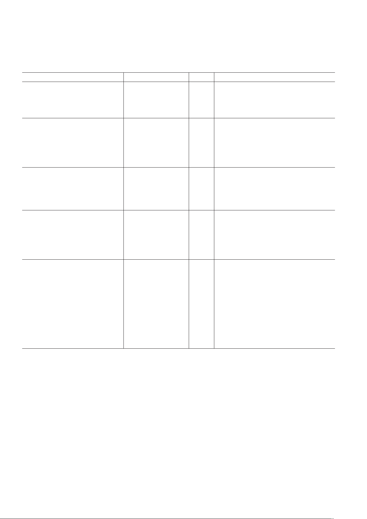
The ADM3222 contains additional enable and shutdown circuitry. The EN input may be used to three-state the receiver
outputs. The SD input is used to power down the charge
pump and transmitter outputs reducing the quiescent current to
less than 0.5 µA. The receivers remain enabled during shutdown
unless disabled using EN.
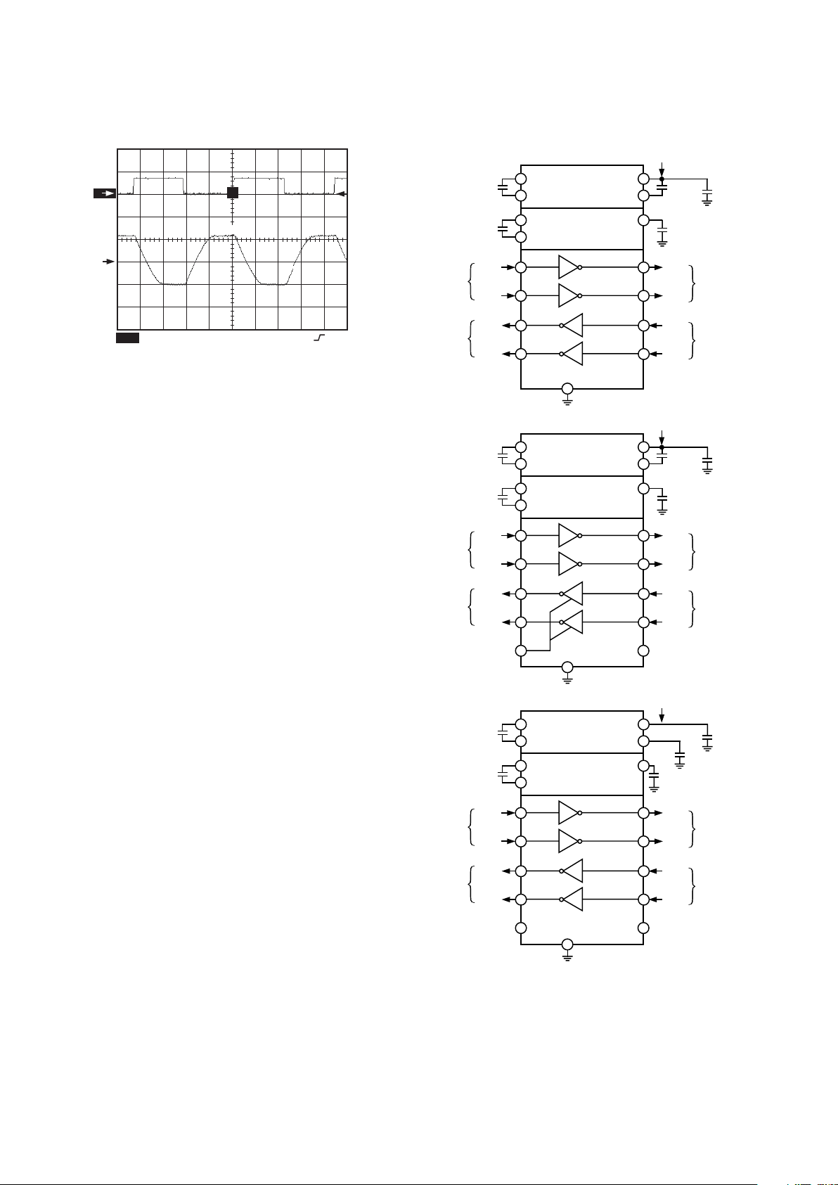
The ADM1385 contains a driver disable mode and a complete
shutdown mode.
The ADM3202 is available in a 16-lead DIP, narrow and wide
SOIC as well as a space saving 16-lead TSSOP package. The
ADM3222 is available in 18-lead DIP, SO and in 20-lead SSOP
and TSSOP. The ADM1385 is available in a 20-lead SSOP
package, which is pin compatible with the LTC1385 CG.
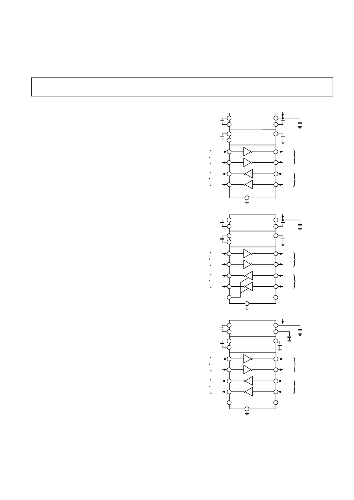
+3.3V TO +6.6V
VOLTAGE
DOUBLER
C1+
C1–
C5
0.1F
+
V
CC
V+
0.1F
10V
+
+
C3
0.1F
6.3V
+3.3V INPUT
+6.6V TO –6.6V
VOLTAGE
INVERTER
C2+
C2–
+
V–
0.1F
10V
+
C4
0.1F
10V
T1
OUT
T1
IN
T2
OUT
T2
IN
EIA/TIA-232
OUTPUTS
R1
OUT
R2
OUT
R1
IN
R2
IN
EIA/TIA-232
INPUTS*
CMOS
INPUTS
CMOS
OUTPUTS
ADM3202
GND
*INTERNAL 5k PULL-DOWN RESISTOR
ON EACH RS-232 INPUT
+3.3V TO +6.6V
VOLTAGE
DOUBLER
C1+
C1–
C5
0.1F
+
V
CC
V+
0.1F
10V
+
+
C3
0.1F
6.3V
+3.3V INPUT
+6.6V TO –6.6V
VOLTAGE
INVERTER
C2+
C2–
+
V–
0.1F
10V
+
C4
0.1F
10V
T1
OUT
T1
IN
T2
OUT
T2
IN
EIA/TIA-232
OUTPUTS
R1
OUT
R2
OUT
R1
IN
R2
IN
EIA/TIA-232
INPUTS*
CMOS
INPUTS
CMOS
OUTPUTS
ADM3222
GND
*INTERNAL 5k PULL-DOWN RESISTOR
ON EACH RS-232 INPUT
T1
T2
R2
R1
T1
T2
R2
R1
EN SD
+3.3V TO +6.6V
VOLTAGE
DOUBLER
C1+
C1–
C5
0.1F
+
V
CC
V+
0.1F
10V
+
C3
0.1F
6.3V
+3.3V INPUT
+6.6V TO –6.6V
VOLTAGE
INVERTER
C2+
C2–
+
V–
0.1F
10V
+
C4
0.1F
10V
T1
OUT
T1
IN
T2
OUT
T2
IN
EIA/TIA-232
OUTPUTS
R1
OUT
R2
OUT
R1
IN
R2
IN
EIA/TIA-232
INPUTS*
CMOS
INPUTS
CMOS
OUTPUTS
ADM1385
GND
*INTERNAL 5k PULL-DOWN RESISTOR
ON EACH RS-232 INPUT
T1
T2
R2
R1
DD
SD
+
–2–
REV. B
ADM3202/ADM3222/ADM1385–SPECIFICATIONS
Parameter Min Typ Max Unit Test Conditions/Comments
DC CHARACTERISTICS
Operating Voltage Range 3.0 3.3 5.5 V
V
CC
Power Supply Current 1.3 3 mA No Load
812 mAR
L
= 3 kΩ to GND
Shutdown Supply Current 0.01 0.5 µA
LOGIC
Input Logic Threshold Low, V
INL
0.8 V T
IN
Input Logic Threshold High, V
INH
2.0 V T
IN
CMOS Output Voltage Low, V
OL
0.4 V I
OUT
= 1.6 mA
CMOS Output Voltage High, V
OH
VCC – 0.6 V I
OUT
= –1 mA
Logic Pull-Up Current 5 10 µAT
IN
= GND to V
CC
*
Output Leakage Current ± 10 µA Receivers Disabled
RS-232 RECEIVER
EIA-232 Input Voltage Range –30 +30 V
EIA-232 Input Threshold Low 0.6 1.2 V
EIA-232 Input Threshold High 1.6 2.4 V
EIA-232 Input Hysteresis 0.4 V
EIA-232 Input Resistance 3 5 7 kΩ
RS-232 TRANSMITTER
Output Voltage Swing (RS-232) ± 5.0 ± 5.2 V V
CC
= 3.3 V. All Transmitter Outputs Loaded
with 3 kΩ to Ground
Output Voltage Swing (RS-562) ± 3.7 V V
CC
= 3.0 V
Transmitter Output Resistance 300 Ω V
CC
= 0 V, V
OUT
= ± 2 V
RS-232 Output Short Circuit Current ± 15 mA
Output Leakage Current ± 25 µA SD = Low, V
OUT
= 12 V
TIMING CHARACTERISTICS
Maximum Data Rate 460 kbps VCC = 3.3 V, RL = 3 kΩ to 7 kΩ, CL = 50 pF to
Receiver Propagation Delay 1000 pF. One Tx Switching
TPHL 0.4 1 µs
TPLH 0.4 1 µs
Transmitter Propagation Delay 300 1.2 µsR
L
= 3 kΩ, CL = 1000 pF
Receiver Output Enable Time 200 ns
Receiver Output Disable Time 200 ns
Transmitter Skew 30 ns
Receiver Skew 300 ns
Transition Region Slew Rate Measured from +3 V to –3 V or –3 V to +3 V,
V
CC
= +3.3 V
5.5 10 30 V/µsR
L
= 3 kΩ, CL = 1000 pF, TA = 25°C
*ADM1385: Input leakage current typically –10 µA when TIN = GND.
Specifications subject to change without notice.
(VCC = 3.3 V 0.3 V, C1–C4 = 0.1 F. All specifications T
MIN
to T
MAX
unless otherwise noted.)

ADM3202/ADM3222/ADM1385
–3–REV. B
ABSOLUTE MAXIMUM RATINGS*
(TA = 25°C unless otherwise noted)
VCC . . . . . . . . . . . . . . . . . . . . . . . . . . . . . . . . . –0.3 V to +6 V
V+ . . . . . . . . . . . . . . . . . . . . . . . . . . . . (V
CC
– 0.3 V) to +14 V
V– . . . . . . . . . . . . . . . . . . . . . . . . . . . . . . . . . +0.3 V to –14 V
Input Voltages
T
IN
. . . . . . . . . . . . . . . . . . . . . . . . . . –0.3 V to (V+, +0.3 V)
R
IN
. . . . . . . . . . . . . . . . . . . . . . . . . . . . . . . . . . . . . . . ± 30 V
Output Voltages
T
OUT
. . . . . . . . . . . . . . . . . . . . . . . . . . . . . . . . . . . . . ± 15 V
R
OUT
. . . . . . . . . . . . . . . . . . . . . . . –0.3 V to (VCC + 0.3 V)
Short Circuit Duration
T
OUT
. . . . . . . . . . . . . . . . . . . . . . . . . . . . . . . . . Continuous
Power Dissipation
Power Dissipation N-16 . . . . . . . . . . . . . . . . . . . . . 450 mW
(Derate 6 mW/°C above 50°C)
θ
JA
, Thermal Impedance . . . . . . . . . . . . . . . . . . . 117°C/W
Power Dissipation R-16 . . . . . . . . . . . . . . . . . . . . . 450 mW
(Derate 6 mW/°C above 50°C)
θ
JA
, Thermal Impedance . . . . . . . . . . . . . . . . . . . 158°C/W
Power Dissipation RU-16 . . . . . . . . . . . . . . . . . . . 500 mW
(Derate 6 mW/°C above 50°C)
θ
JA
, Thermal Impedance . . . . . . . . . . . . . . . . . . . 158°C/W
Power Dissipation R-18 . . . . . . . . . . . . . . . . . . . . . 450 mW
(Derate 6 mW/°C above 50°C)
θ
JA
, Thermal Impedance . . . . . . . . . . . . . . . . . . . 158°C/W
Power Dissipation RS-20 . . . . . . . . . . . . . . . . . . . . 450 mW
(Derate 6 mW/°C above 50°C)
θ
JA
, Thermal Impedance . . . . . . . . . . . . . . . . . . . 158°C/W
Power Dissipation RU-20 . . . . . . . . . . . . . . . . . . . 450 mW
(Derate 6 mW/°C above 50°C)
θ
JA
, Thermal Impedance . . . . . . . . . . . . . . . . . . . 158°C/W
Operating Temperature Range
Industrial (A Version) . . . . . . . . . . . . . . . . – 40°C to +85°C
Storage Temperature Range . . . . . . . . . . . . –65°C to +150°C
Lead Temperature (Soldering, 10 sec) . . . . . . . . . . . . . . 300°C
*This is a stress rating only; functional operation of the device at these or any other
conditions above those indicated in the operation sections of this specification
is not implied. Exposure to absolute maximum rating conditions for extended
periods of time may affect reliability.
ORDERING GUIDE
Model Temperature Range Package Options*
ADM3202AN –40°C to +85°C N-16
ADM3202ARN – 40°C to +85°C R-16A
ADM3202ARW –40°C to +85°C R-16
ADM3202ARU –40°C to +85°C RU-16
ADM3222AN –40°C to +85°C N-18
ADM3222ARW –40°C to +85°C R-18
ADM3222ARS –40°C to +85°C RS-20
ADM3222ARU –40°C to +85°C RU-20
ADM1385ARS –40°C to +85°C RS-20
*N = Plastic DIP; R = Small Outline; RS = Shrink Small Outline; RU = Thin
Shrink Small Outline.

ADM3202/ADM3222/ADM1385
–4–
REV. B
PIN FUNCTION DESCRIPTIONS
Mnemonic Function
V
CC
Power Supply Input: 3.3 V ± 0.3 V.
V+ Internally Generated Positive Supply
(+6 V Nominal).
V– Internally Generated Negative Supply
(–6 V Nominal).
GND Ground Pin. Must be connected to 0 V.
C1+, C1– External Capacitor 1 is connected between these
pins. 0.1 µF capacitor is recommended but larger
capacitors up to 47 µF may be used.
C2+, C2– External Capacitor 2 is connected between these
pins. 0.1 µF capacitor is recommended but larger
capacitors up to 47 µF may be used.
Tx
IN
Transmitter (Driver) Inputs. These inputs accept
TTL/CMOS levels.
Tx
OUT
Transmitter (Driver) Outputs. These are RS-232
signal levels (typically ±9 V).
Rx
IN
Receiver Inputs. These inputs accept RS-232
signal levels. An internal 5 kΩ pull-down resistor
to GND is connected on each input.
Rx
OUT
Receiver Outputs. These are CMOS output logic
levels.
EN (ADM3222) Receiver Enable, Active Low. When
low, the receiver outputs are enabled. When high,
they are three-stated.
SD (ADM3222) Shutdown Control. Active Low.
When low, the charge pump is shut down and
the transmitter outputs are disabled.
SD (ADM1385) Shutdown Control. When low, the
charge pump is shut down and all transmitters
and receivers are disabled.
DD (ADM1385) Driver Disable. When low, the
charge pump is turned off and the transmitters
are disabled. The receivers remain active.
PIN CONNECTIONS DIP (N, R Packages)
PIN CONNECTIONS DIP (RS, RU Packages)
TOP VIEW
(Not to Scale)
16
15
14
13
12
11
10
9
1
2
3
4
5
6
7
8
C1+
V+
C1–
C2+
C2–
V–
T2
OUT
R2
IN
V
CC
GND
T1
OUT
R1
IN
R1
OUT
T1
IN
T2
IN
R2
OUT
ADM3202
TOP VIEW
(Not to Scale)
18
17
16
15
14
13
12
11
10
1
2
3
4
5
6
7
8
9
ADM3222
R2
IN
T2
OUT
EN
C1+
V+
C1–
V–
C2–
C2+
T2
IN
SD
V
CC
GND
T1
OUT
T1
IN
R1
OUT
R1
IN
R2
OUT
TOP VIEW
(Not to Scale)
20
19
18
17
16
15
14
13
12
11
1
2
3
4
5
6
7
8
9
10
ADM1385
(SSOP)
NC = NO CONNECT
NC
R2
IN
T2
OUT
C1+
V+
C1–
V–
C2–
C2+
NC
T2
IN
T1
IN
V
CC
GND
T1
OUT
R2
OUT
R1
OUT
R1
IN
DD
SD
TOP VIEW
(Not to Scale)
20
19
18
17
16
15
14
13
12
11
1
2
3
4
5
6
7
8
9
10
ADM3222
(SSOP
TSSOP)
NC = NO CONNECT
R2
OUT
R2
IN
T2
OUT
C1+
V+
C1–
V–
C2–
C2+
NC
T2
IN
T1
IN
V
CC
GND
T1
OUT
NC
R1
OUT
R1
IN
EN
SD

ADM3202/ADM3222/ADM1385
–5–REV. B
LOAD CAPACITANCE – pF
8
6
4
2
0
–2
–4
–6
–8
0 1200200 400 600 800
T
OUT
(HIGH)
T
OUT
(LOW)
Tx O/P VOLTAGE – V
1000
TPC 1. Transmitter Output Voltage High/Low vs. Load
Capacitance @ 460 kbps
VCC – V
8
2.7 2.9 3.1 3.3 3.5
Tx O/P HIGH
Tx O/P – V
6
4
2
0
–2
–4
–6
–8
Tx O/P LOW
TPC 2. Transmitter Output Voltage vs. V
CC
LOAD CURRENT – mA
8
02468
Tx O/P – V
6
4
2
0
–2
–4
–6
–8
10 12
Tx O/P LOW
Tx O/P HIGH
TPC 3. Transmitter Output Voltage Low/High vs. Load
Current
TPC 4. Charge Pump V+, V– vs. Load Current
VCC – V
350
2.7 2.9 3.1 3.3 3.5
IMPEDANCE –
300
250
200
150
100
50
0
V+ (IMPEDANCE)
V– (IMPEDANCE)
TPC 5. Charge Pump Impedance vs. V
CC
LOAD CAPACITANCE – pF
20
0 1000 2000 3000
I
CC
@ 230kbps
I
CC
– mA
18
16
14
12
10
2
0
8
6
4
I
CC
@ 460kbps
TPC 6. Power Supply Current vs. Load Capacitance
Typical Performance Characteristics–
LOAD CURRENT – mA
8
02468
V+
V+, V– – V
6
4
2
0
–2
–4
–6
–8
V–
10 12
ADM3202/ADM3222/ADM1385
–6–
REV. B
GENERAL DESCRIPTION
The ADM3202/ADM3222/ADM1385 are RS-232 line drivers/
receivers. Step-up voltage converters coupled with level shifting
transmitters and receivers allow RS-232 levels to be developed
while operating from a single 3.3 V supply.
CMOS technology is used to keep the power dissipation to an
absolute minimum, allowing maximum battery life in portable
applications.
The ADM3202/ADM3222/ADM1385 is a modification, enhancement and improvement to the AD230–AD241 family and its
derivatives. It is essentially plug-in compatible and does not
have materially different applications.
CIRCUIT DESCRIPTION
The internal circuitry consists of three main sections. These are:
1. A charge pump voltage converter
2. 3.3 V logic to EIA-232 transmitters
3. EIA-232 to 5 V logic receivers.
Charge Pump DC-DC Voltage Converter
The charge pump voltage converter consists of a 200 kHz oscillator and a switching matrix. The converter generates a ±6.6 V
supply from the input 3.3 V level. This is done in two stages
using a switched capacitor technique as illustrated below. First,
the 3.3 V input supply is doubled to 6.6 V using capacitor C1 as
the charge storage element. The +6.6 V level is then inverted
to generate –6.6 V using C2 as the storage element. C3 is shown
connected between V+ and V
CC
, but is equally effective if con-
nected between V+ and GND.
Capacitors C3 and C4 are used to reduce the output ripple.
Their values are not critical and can be increased if desired.
Capacitor C3 is shown connected between V+ and V
CC
. It is
also acceptable to connect this capacitor between V+ and GND.
If desired, larger capacitors (up to 10 µF) can be used for
capacitors C1–C4.
+3.3V TO +6.6V
VOLTAGE
DOUBLER
C1+
C1–
C5
0.1F
+
V
CC
V+
0.1F
10V
+
+
C3
0.1F
6.3V
+3.3V INPUT
+6.6V TO –6.6V
VOLTAGE
INVERTER
C2+
C2–
+
V–
0.1F
10V
+
C4
0.1F
10V
T1
OUT
T1
IN
T2
OUT
T2
IN
EIA/TIA-232
OUTPUTS
R1
OUT
R2
OUT
R1
IN
R2
IN
EIA/TIA-232
INPUTS*
CMOS
INPUTS
CMOS
OUTPUTS
ADM3202
GND
*INTERNAL 5k PULL-DOWN RESISTOR
ON EACH RS-232 INPUT
+3.3V TO +6.6V
VOLTAGE
DOUBLER
C1+
C1–
C5
0.1F
+
V
CC
V+
0.1F
10V
+
+
C3
0.1F
6.3V
+3.3V INPUT
+6.6V TO –6.6V
VOLTAGE
INVERTER
C2+
C2–
+
V–
0.1F
10V
+
C4
0.1F
10V
T1
OUT
T1
IN
T2
OUT
T2
IN
EIA/TIA-232
OUTPUTS
R1
OUT
R2
OUT
R1
IN
R2
IN
EIA/TIA-232
INPUTS*
CMOS
INPUTS
CMOS
OUTPUTS
ADM3222
GND
*INTERNAL 5k PULL-DOWN RESISTOR
ON EACH RS-232 INPUT
T1
T2
R2
R1
T1
T2
R2
R1
EN SD
+3.3V TO +6.6V
VOLTAGE
DOUBLER
C1+
C1–
C5
0.1F
+
V
CC
V+
0.1F
10V
+
C3
0.1F
6.3V
+3.3V INPUT
+6.6V TO –6.6V
VOLTAGE
INVERTER
C2+
C2–
+
V–
0.1F
10V
+
C4
0.1F
10V
T1
OUT
T1
IN
T2
OUT
T2
IN
EIA/TIA-232
OUTPUTS
R1
OUT
R2
OUT
R1
IN
R2
IN
EIA/TIA-232
INPUTS*
CMOS
INPUTS
CMOS
OUTPUTS
ADM1385
GND
*INTERNAL 5k PULL-DOWN RESISTOR
ON EACH RS-232 INPUT
T1
T2
R2
R1
DD
SD
+
Figure 1. Typical Operating Circuits
1
CH 1 5.00V CH 2 5.00V M 1.00sCH 1 0V
T
2
T
TPC 7. 460 kbps Data Transmission

ADM3202/ADM3222/ADM1385
–7–REV. B
OUTLINE DIMENSIONS
Dimensions shown in inches and (mm).
16-Lead Plastic DIP
(N-16)
16
1
8
9
PIN 1
0.840 (21.34)
0.745 (18.92)
0.280 (7.11)
0.240 (6.10)
SEATING
PLANE
0.060 (1.52)
0.015 (0.38)
0.210 (5.33)
MAX
0.022 (0.558)
0.014 (0.356)
0.160 (4.06)
0.115 (2.93)
0.100
(2.54)
BSC
0.070 (1.77)
0.045 (1.15)
0.130
(3.30)
MIN
0.195 (4.95)
0.115 (2.93)
0.015 (0.381)
0.008 (0.204)
0.325 (8.25)
0.300 (7.62)
16-Lead Thin Shrink Small Outline (TSSOP)
(RU-16)
16
9
81
0.256 (6.50)
0.246 (6.25)
0.177 (4.50)
0.169 (4.30)
PIN 1
0.201 (5.10)
0.193 (4.90)
SEATING
PLANE
0.006 (0.15)
0.002 (0.05)
0.0118 (0.30)
0.0075 (0.19)
0.0256 (0.65)
BSC
0.0433 (1.10)
MAX
0.0079 (0.20)
0.0035 (0.090)
0.028 (0.70)
0.020 (0.50)
8
0
16-Lead Narrow Body SOIC
(R-16A)
16
9
8
1
0.1574 (4.00)
0.1497 (3.80)
0.3937 (10.00)
0.3859 (9.80)
0.050 (1.27)
BSC
PIN 1
0.2440 (6.20)
0.2284 (5.80)
SEATING
PLANE
0.0098 (0.25)
0.0040 (0.10)
0.0192 (0.49)
0.0138 (0.35)
0.0688 (1.75)
0.0532 (1.35)
8
0
0.0196 (0.50)
0.0099 (0.25)
45
0.0500 (1.27)
0.0160 (0.41)
0.0099 (0.25)
0.0075 (0.19)
16-Lead Wide Body SOIC
(R-16)
SEATING
PLANE
0.0118 (0.30)
0.0040 (0.10)
0.0192 (0.49)
0.0138 (0.35)
0.1043 (2.65)
0.0926 (2.35)
0.050 (1.27)
BSC
16 9
81
0.4193 (10.65)
0.3937 (10.00)
0.2992 (7.60)
0.2914 (7.40)
PIN 1
0.4133 (10.50)
0.3977 (10.00)
0.0125 (0.32)
0.0091 (0.23)
8
0
0.0291 (0.74)
0.0098 (0.25)
45
0.0500 (1.27)
0.0157 (0.40)
C1
+
C3
+
S3
S4
S1
S2
INTERNAL
OSCILLATOR
V
CC
GND
V
CC
V+ = 2V
CC
Figure 2. Charge Pump Voltage Doubler
C2
+
C4
+
S3
S4
S1
S2
INTERNAL
OSCILLATOR
V
+
GND
V– = –(V+)
GND
FROM
VOLTAGE
DOUBLER
Figure 3. Charge Pump Voltage Inverter
Transmitter (Driver) Section
The drivers convert 3.3 V logic input levels into RS-232 output
levels. With V
CC
= 3.3 V and driving an RS-232 load, the out-
put voltage swing is typically ±6 V.
Receiver Section
The receivers are inverting level-shifters that accept RS-232
input levels and translate them into 3 V logic output levels.
The inputs have internal 5 kΩ pull-down resistors to ground and
are also protected against overvoltages of up to ±30 V. Unconnected inputs are pulled to 0 V by the internal 5 kΩ pull-down
resistor. This, therefore, results in a Logic 1 output level for
unconnected inputs or for inputs connected to GND.
The receivers have Schmitt trigger inputs with a hysteresis level
of 0.4 V. This ensures error-free reception for both noisy inputs
and for inputs with slow transition times.
HIGH BAUD RATE
The ADM3202E/ADM3222E feature high slew rates permitting
data transmission at rates well in excess of the EIA/RS-232E
specifications. RS-232 voltage levels are maintained at data rates
up to 460 kbps even under worst case loading conditions. This
allows for high speed data links between two terminals or indeed
it is suitable for the new generation I
SDN
modem standards which
requires data rates of 230 kbps. The slew rate is internally controlled to less than 30 V/µs in order to minimize EMI interference.

ADM3202/ADM3222/ADM1385
–8–
REV. B
C00071–0–12/01(B)
PRINTED IN U.S.A.
20-Lead Thin Shrink Small Outline (TSSOP)
(RU-20)
20
1
11
10
0.256 (6.50)
0.246 (6.25)
0.177 (4.50)
0.169 (4.30)
PIN 1
0.260 (6.60)
0.252 (6.40)
SEATING
PLANE
0.006 (0.15)
0.002 (0.05)
0.0118 (0.30)
0.0075 (0.19)
0.0256 (0.65)
BSC
0.0433 (1.10)
MAX
0.0079 (0.20)
0.0035 (0.090)
0.028 (0.70)
0.020 (0.50)
8
0
18-Lead Plastic DIP
(N-18)
SEATING
PLANE
0.060 (1.52)
0.015 (0.38)
0.210 (5.33)
MAX
0.022 (0.558)
0.014 (0.356)
0.160 (4.06)
0.115 (2.93)
0.100
(2.54)
BSC
0.070 (1.77)
0.045 (1.15)
0.130
(3.30)
MIN
18
19
10
PIN 1
0.925 (23.49)
0.845 (21.47)
0.280 (7.11)
0.240 (6.10)
0.195 (4.95)
0.115 (2.93)
0.015 (0.381)
0.008 (0.204)
0.325 (8.25)
0.300 (7.62)
18-Lead Wide Body SOIC
(R-18)
SEATING
PLANE
0.0118 (0.30)
0.0040 (0.10)
0.0192 (0.49)
0.0138 (0.35)
0.1043 (2.65)
0.0926 (2.35)
0.0500
(1.27)
BSC
18 10
9
1
0.4193 (10.65)
0.3937 (10.00)
0.2992 (7.60)
0.2914 (7.40)
PIN 1
0.4625 (11.75)
0.4469 (11.35)
0.0125 (0.32)
0.0091 (0.23)
8
0
0.0291 (0.74)
0.0098 (0.25)
45
0.0500 (1.27)
0.0157 (0.40)
20-Lead Shrink Small Outline (SSOP)
(RS-20)
0.037 (0.94)
0.022 (0.559)
0.009 (0.229)
0.005 (0.127)
8
0
0.295 (7.50)
0.271 (6.90)
0.311 (7.9)
0.301 (7.64)
0.212 (5.38)
0.205 (5.21)
20 11
10
1
PIN 1
0.0256
(0.65)
BSC
0.008 (0.203)
0.002 (0.050)
0.07 (1.78)
0.066 (1.67)
0.078 (1.98)
0.068 (1.73)
SEATING
PLANE
Revision History
Location Page
11/01—Data Sheet changed from REV. A to REV. B.
Changes to Specifications page . . . . . . . . . . . . . . . . . . . . . . . . . . . . . . . . . . . . . . . . . . . . . . . . . . . . . . . . . . . . . . . . . . . . . . . . . . . . . 2
 Loading...