Isolated CAN Transceiver with Integrated
V
High Voltage, Bus-Side, Linear Regulator
FEATURES
5 kV rms isolated CAN transceiver
Integrated V
Bus side powered by V
11 V to 25 V operation on V
5 V or 3.3 V operation on V
Complies with ISO 11898 standard
High speed data rates up to 1 Mbps
Short-circuit protection on bus pins
Integrated bus miswire protection
Unpowered nodes do not disturb the bus
110 or more nodes on the bus
Thermal shutdown protection
High common-mode transient immunity: >25 kV/μs
Safety and regulatory approvals
UL recognition (pending)
5000 V
VDE Certificates of Conformity (pending)
DIN V VDE V 0884-10 (VDE V 0884-10):2006-12
V
Industrial operating temperature range: −40°C to +85°C
Wide body, 16-lead SOIC package
linear regulator
+
for 1 minute per UL 1577
RMS
= 846 V peak
IORM
and V
+
+
DD1
−
ADM3052
GENERAL DESCRIPTION
The ADM3052 is an isolated controller area network (CAN)
physical layer transceiver with a V
The ADM3052 complies with the ISO 11898 standard.
The device employs Analog Devices, Inc., iCoupler® technology
to combine a 3-channel isolator, a CAN transceiver, and a linear
regulator into a single package. The power is isolated between a
single 3.3 V or 5 V supply on V
24 V supply provided on V
+
The ADM3052 creates an isolated interface between the CAN
protocol controller and the physical layer bus. It is capable of
running at data rates up to 1 Mbps.
The device has integrated miswire protection on the bus pins,
V
, V−, CANH, and CANL.
+
The device has current-limiting and thermal shutdown features
to protect against output short circuits and situations where the
bus may be shorted to ground or power terminals. The part
is fully specified over the industrial temperature range and is
available in a 16-lead, wide-body SOIC package.
integrated linear regulator.
+
, the logic side, and a single
DD1
, the bus side.
APPLICATIONS
CAN data buses
Industrial field networks
DeviceNet applications
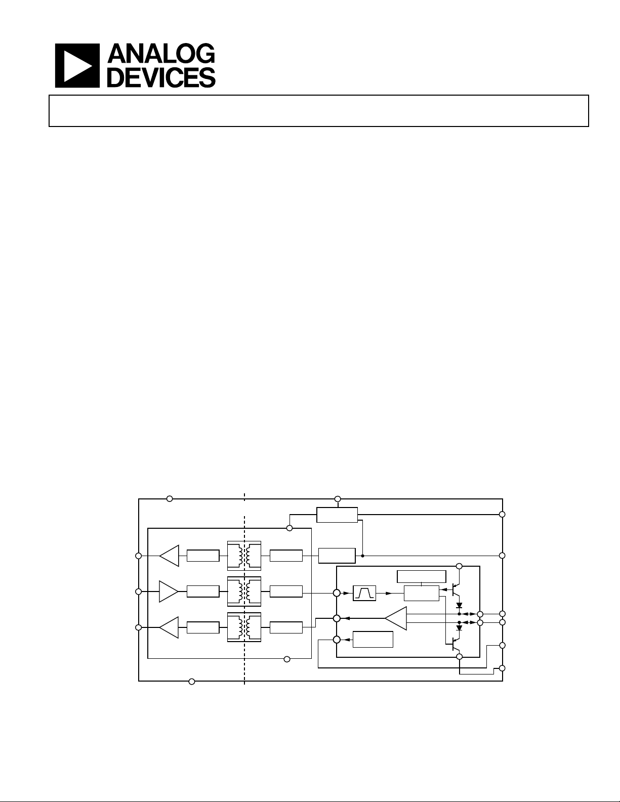
FUNCTIONAL BLOCK DIAGRAM
DD1
ISOLATION
BARRIER
V
DD2
V
+SENSE
TxD
RxD
Rev. 0
Information furnished by Analog Devices is believed to be accurate and reliable. However, no
responsibility is assumed by Analog Devices for its use, nor for any infringements of patents or other
rights of third parties that may result from its use. Specifications subject to change without notice. No
license is granted by implication or otherwise under any patent or patent rights of Analog Devices.
Trademarks and registered trademarks are the property of their respective owners.
DECODE ENCODE
ENCODE
DECODE
DIGITAL ISOLATION
GND
1
LOGIC SIDE
DECODE
ENCODE
GND
ADM3052
2
C
INT
LINEAR
REGULATOR
BUS
V
+SENSE
TxD
RxD
V
REF
BUS SIDE
RECEIVER
REFERENCE
VOLTAGE
CAN TRANSCEI V E R
PROTECTION
DRIVER
GND
V
DD2
2
V
+R
V
+
CANH
CANL
V
REF
V
–
Figure 1.
One Technology Way, P.O. Box 9106, Norwood, MA 02062-9106, U.S.A.
Tel: 781.329.4700 www.analog.com
Fax: 781.461.3113 ©2011 Analog Devices, Inc. All rights reserved.
09292-001

ADM3052
TABLE OF CONTENTS
Features .............................................................................................. 1
Applications ....................................................................................... 1
General Description ......................................................................... 1
Functional Block Diagram .............................................................. 1
Revision History ............................................................................... 2
Specifications ..................................................................................... 3
Timing Specifications .................................................................. 4
Regulatory Information ............................................................... 4
Insulation and Safety-Related Specifications ............................ 4
VDE 0884 Insulation Characteristics (Pending) ...................... 5
Absolute Maximum Ratings ............................................................ 6
ESD Caution .................................................................................. 6
Pin Configuration and Function Descriptions ............................. 7
Typical Performance Characteristics ............................................. 8
Test Circuits ..................................................................................... 12
Switching Characteristics .............................................................. 13
Circuit Description......................................................................... 14
CAN Transceiver Operation ..................................................... 14
Electrical Isolation ...................................................................... 14
Truth Tables................................................................................. 14
Thermal Shutdown .................................................................... 16
Linear Regulator ......................................................................... 16
Magnetic Field Immunity .......................................................... 16
Applications Information .............................................................. 17
Typical Applications ................................................................... 17
Outline Dimensions ....................................................................... 18
Ordering Guide .......................................................................... 18
REVISION HISTORY
6/11—Revision 0: Initial Version
Rev. 0 | Page 2 of 20

ADM3052
SPECIFICATIONS
All voltages are relative to their respective ground; 3.0 V ≤ V
Table 1.
Parameter Symbol Min Typ Max Unit Test Conditions
SUPPLY CURRENT
Power Supply Current Logic Side
TxD/RxD Data Rate 1 Mbps I
0.7 2 mA
DD1
Power Supply Current Bus Side
Recessive State I+ 10 mA RL = 60 Ω, see Figure 26
Dominant State I+ 64 75 mA RL = 60 Ω, see Figure 26
TxD/RxD Data Rate 1 Mbps I+ 48 55 mA RL = 60 Ω, see Figure 26
EXTERNAL RESISTOR
Resistance RP 297 300 303 Ω
Power Rating 0.75 W
DRIVER
Logic Inputs
Input Voltage High VIH 0.7 V
Input Voltage Low VIL 0.25 V
CMOS Logic Input Currents IIH, IIL 500 μA TxD
Differential Outputs
Recessive Bus Voltage V
CANH Output Voltage V
CANL Output Voltage V
, V
CANL
CANH
0.5 2.0 V V
CANL
2.0 3.0 V V
CANH
2.75 4.5 V V
Differential Output Voltage VOD 1.5 3.0 V V
V
Short-Circuit Current, CANH I
−500 +50 mV V
OD
−200 mA V
SCCANH
−100 mA V
Short-Circuit Current, CANL I
200 mA V
SCCANL
RECEIVER
Differential Inputs
Voltage Recessive V
Voltage Dominant V
Input Voltage Hysteresis V
−1.0 +0.5 V
IDR
0.9 5.0 V
IDD
150 mV See Figure 24
HYS
CANH, CANL Input Resistance RIN 5 25 kΩ
Differential Input Resistance R
20 100 kΩ
DIFF
Logic Outputs
Output Low Voltage VOL 0.2 0.4 V I
Output High Voltage VOH V
Short-Circuit Current IOS 7 85 mA V
VOLTAGE REFERENCE
Reference Output Voltage V
2.025 3.025 V |I
REF
BUS VOLTAGE SENSE
V
Output Voltage Low VOL 0.2 0.4 V I
+SENSE
V
Output Voltage High VOH V
+SENSE
Threshold Voltage V
COMMON-MODE TRANSIENT
IMMUNITY
1
CM is the maximum common-mode voltage slew rate that can be sustained while maintaining specification-compliant operation. VCM is the common-mode potential
difference between the logic and bus sides. The transient magnitude is the range over which the common mode is slewed. The common-mode voltage slew rates
apply to both rising and falling common-mode voltage edges.
1
7.0 10 V
+SENSETH
25 kV/μs V
≤ 5.5 V, TA = −40°C to +85°C, V+ = 11 V to 25 V, unless otherwise noted.
DD1
V TxD
DD1
V TxD
DD1
= high, RL = ∞, see Figure 23
TxD
= low, see Figure 23
TxD
= low, see Figure 23
TxD
= low, RL = 45 Ω, see Figure 23
TxD
= high, RL = ∞, see Figure 23
TxD
= −5 V
CANH
= −36 V
CANH
= 36 V
CANL
, V
< 12 V, see Figure 24,
CANH
, V
< 12 V, see Figure 24,
CANH
DD1
− 0.3 V
DD1
− 0.3 V
DD1
− 0.2 V I
DD1
− 0.2 V I
DD1
−7 V < V
C
−7 V < V
C
CANL
= 15 pF
L
CANL
= 15 pF
L
= 1.5 mA
OUT
= −1.5 mA
OUT
= GND1 or V
OUT
= 50 μA|
REF
= 1.5 mA
O+SENSE
= −1.5 mA
O+SENSE
= 1 kV, transient magnitude = 800 V
CM
Rev. 0 | Page 3 of 20

ADM3052
TIMING SPECIFICATIONS
All voltages are relative to their respective ground; 3.0 V ≤ V
Table 2.
Parameter Symbol Min Typ Max Unit Test Conditions
DRIVER
Maximum Data Rate 1 Mbps
Propagation Delay from TxD On to Bus Active t
Propagation Delay from TxD Off to Bus Inactive t
RECEIVER
Propagation Delay from TxD On to Receiver Active t
Propagation Delay from TxD Off to Receiver Inactive t
POWER-UP
Enable Time, V+ High to V
Disable Time, V+ Low to V
Low tSE 300 μs See Figure 29
+SENSE
High tSD 10 ms See Figure 29
+SENSE
REGULATORY INFORMATION
The ADM3052 approval is pending by the organizations listed in Table 3.
≤ 5.5 V, TA = −40°C to +85°C, V+ = 11 V to 25 V, unless otherwise noted.
DD1
90 ns
onTxD
See Figure 25 and Figure 27,
RL = 60 Ω, CL = 100 pF
120 ns
offTxD
200 ns
onRxD
250 ns
offRxD
See Figure 25 and Figure 27,
= 60 Ω, CL = 100 pF
R
L
See Figure 25 and Figure 27,
= 60 Ω, CL = 100 pF
R
L
See Figure 25 and Figure 27,
= 60 Ω, CL = 100 pF
R
L
Table 3.
Organization Approval Type Notes
UL
Recognized under the component recognition
program of Underwriters Laboratories, Inc.
In accordance with UL 1577, each ADM3052 is proof tested by
applying an insulation test voltage ≥6000 V rms for 1 second
(current leakage detection limit = 10 μA)
VDE
Certified according to DIN V VDE V 0884-10
(VDE V 0884-10):2006-12
In accordance with DIN V VDE V 0884-10, each ADM3052 is proof
tested by applying an insulation test voltage ≥1590 V peak for
1 second (partial discharge detection limit = 5 pC)
INSULATION AND SAFETY-RELATED SPECIFICATIONS
Table 4.
Parameter Symbol Value Unit Conditions
Rated Dielectric Insulation Voltage 5000 V rms 1-minute duration
Minimum External Air Gap (Clearance) L(I01) 7.7 mm
Minimum External Tracking (Creepage) L(I02) 7.6 mm
Minimum Internal Gap (Internal Clearance) 0.017 min mm Insulation distance through insulation
Tracking Resistance (Comparative Tracking Index) CTI >175 V DIN IEC 112/VDE 0303-1
Isolation Group IIIa Material group (DIN VDE 0110)
Measured from input terminals to output terminals,
shortest distance through air
Measured from input terminals to output terminals,
shortest distance along body
Rev. 0 | Page 4 of 20

ADM3052
VDE 0884 INSULATION CHARACTERISTICS (PENDING)
This isolator is suitable for reinforced electrical isolation within the safety limit data. Maintenance of the safety data must be ensured by
means of protective circuits.
Table 5.
Description Test Conditions Symbol Characteristic Unit
CLASSIFICATIONS
Installation Classification per DIN VDE 0110 for Rated
Mains Voltage
≤150 V rms I to IV
≤300 V rms I to III
≤400 V rms I to II
Climatic Classification 40/85/21
Pollution Degree DIN VDE 0110 2
VOLTAGE
Maximum Working Insulation Voltage V
Input-to-Output Test Voltage, Method B1
× 1.875 = VPR, 100% production tested,
V
IORM
= 1 sec, partial discharge < 5 pC
t
m
Input-to-Output Test Voltage, Method A VPR 1357 V peak
After Environmental Tests, Subgroup 1
× 1.6 = VPR, tm = 60 sec,
V
IORM
partial discharge < 5 pC
After Input and/or Safety Test,
Subgroup 2/Subgroup 3
V
× 1.2 = VPR, tm = 60 sec,
IORM
partial discharge < 5 pC
Highest Allowable Overvoltage VTR 6000 V peak
SAFETY-LIMITING VALUES
Case Temperature TS 150 °C
Input Current I
Output Current I
Insulation Resistance at TS R
846 V peak
IORM
1590 V peak
V
PR
1018 V peak
265 mA
S, INPUT
335 mA
S, OUTPUT
>109 Ω
S
Rev. 0 | Page 5 of 20

ADM3052
ABSOLUTE MAXIMUM RATINGS
TA = 25°C, unless otherwise noted. All voltages are relative to
their respective ground.
Table 6.
Parameter Rating
V
−0.5 V to +6 V
DD1
V+ −36 V to +36 V
V+R −36 V to +36 V
Digital Input Voltage
TxD −0.5 V to V
Digital Output Voltage
RxD −0.5 V to V
V
−0.5 V to V
+SENSE
CANH, CANL −36 V to +36 V
V
−0.5 V to +6 V
REF
Operating Temperature Range −40°C to +85°C
Storage Temperature Range −55°C to +150°C
ESD (Human Body Model)
3 kV
Lead Temperature
Soldering (10 sec) 300°C
Vapor Phase (60 sec) 215°C
Infrared (15 sec) 220°C
θJA, Thermal Impedance 53°C/W
TJ, Junction Temperature 130°C
+ 0.5 V
DD1
+ 0.5 V
DD1
+ 0.5 V
DD1
Stresses above those listed under Absolute Maximum Ratings
may cause permanent damage to the device. This is a stress
rating only; functional operation of the device at these or any
other conditions above those indicated in the operational
section of this specification is not implied. Exposure to absolute
maximum rating conditions for extended periods may affect
device reliability.
ESD CAUTION
Rev. 0 | Page 6 of 20
 Loading...