

High Speed Industrial CAN Transceiver
V
with Bus Protection for 24 V Systems
Data Sheet
FEATURES
Physical layer CAN transceiver
5 V operation on V
Complies with ISO 11898 standard
High speed data rates up to 1 Mbps
Short-circuit protection on CANH and CANL against shorts to
power/ground in 24 V systems
Unpowered nodes do not disturb the bus
Connect 110 or more nodes on the bus
Slope control for reduced EMI
Thermal shutdown protection
Low current standby mode
Industrial operating temperature range (−40°C to +125°C)
Available in 8-lead SOIC package
APPLICATIONS
CAN data buses
Industrial field networks
DeviceNet applications
CanOpen, CanKingdom
CC
ADM3051
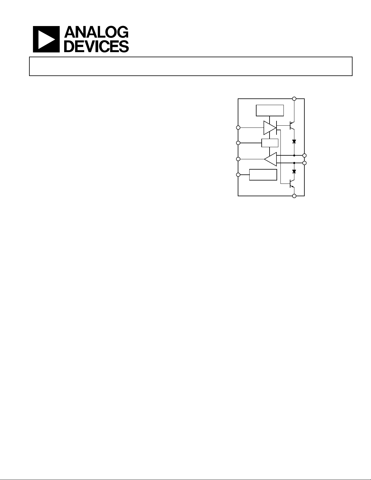
FUNCTIONAL BLOCK DIAGRAM
CC
THERMAL
SHUTDOWN
V
TxD
RS
RxD
REF
ADM3051
D
MODE
VOLTAGE
REFERENCE
Figure 1.
R
CANH
CANL
GND
10029-001
GENERAL DESCRIPTION
The ADM3051 is a controller area network (CAN) physical
layer transceiver allowing a protocol layer CAN controller to
access the physical layer bus. The ADM3051 complies with
the ISO 11898 standard. It is capable of running at data rates up
to 1 Mbps.
The device has current-limiting and thermal shutdown features
to protect against output short circuits and situations where the
bus may be shorted to ground or power terminals in 24 V bus
power systems. The part is fully specified over the industrial
temperature range of −40°C to +125°C and is available in an
8-lead SOIC package.
Three operating modes are available: high speed, slope control,
and standby. Pin 8 (RS) is used to select the operating mode.
The low current standby mode can be selected by applying a
logic high to RS.
The device can be set to operate with slope control to limit EMI
by connecting RS with a resistor to ground to modify the rise
and fall of slopes. This mode facilitates the use of unshielded
cables. Alternatively, disabling slope control by connecting RS
to ground allows high speed operation. Shielded cables or other
measures to control EMI are necessary in this mode.
Rev. 0
Information furnished by Analog Devices is believed to be accurate and reliable. However, no
responsibility is assumed by Analog Devices for its use, nor for any infringements of patents or other
rights of third parties that may result from its use. Specifications subject to change without notice. No
license is granted by implication or otherwise under any patent or patent rights of Analog Devices.
Trademarks and registered trademarks are the property of their respective owners.
One Technology Way, P.O. Box 9106, Norwood, MA 02062-9106, U.S.A.
Tel: 781.329.4700 www.analog.com
Fax: 781.461.3113 ©2011 Analog Devices, Inc. All rights reserved.

ADM3051 Data Sheet
TABLE OF CONTENTS
Features.............................................................................................. 1
Applications....................................................................................... 1
Functional Block Diagram .............................................................. 1
General Description ......................................................................... 1
Revision History ............................................................................... 2
Specifications..................................................................................... 3
Timing Specifications .................................................................. 4
Absolute Maximum Ratings............................................................ 5
ESD Caution.................................................................................. 5
Pin Configuration and Function Descriptions............................. 6
REVISION HISTORY
9/11—Revision 0: Initial Revision
Typical Performance Characteristics..............................................7
Test Circuits and Switching Characteristics................................ 11
Circuit Description......................................................................... 13
CAN Transceiver Operation..................................................... 13
Operational Modes .................................................................... 13
Truth Tables................................................................................. 13
Thermal Shutdown .................................................................... 13
Applications Information.............................................................. 14
Outline Dimensions....................................................................... 15
Ordering Guide............................................................................... 15
Rev. 0 | Page 2 of 16

Data Sheet ADM3051
SPECIFICATIONS
All voltages relative to ground (Pin 2); 4.5 V ≤ VCC ≤ 5.5 V. TA = −40°C to +125°C, RL = 60 Ω, IRS > −10 μA, unless otherwise noted. All
typical specifications are at T
Table 1.
Parameter Symbol Min Typ Max Unit Test Conditions
SUPPLY CURRENT ICC
Dominant State 78 mA V
Recessive State 10 mA V
Standby State 275 µA VRS = VCC, I
DRIVER
Logic Inputs
Input Voltage High VIH 0.7 VCC VCC + 0.3 V Output recessive
Input Voltage Low VIL −0.3 +0.3 VCC V Output dominant
CMOS Logic Input Current High IIH −200 +30 µA V
CMOS Logic Input Current Low IIL −100 −600 µA V
Differential Outputs
Recessive Bus Voltage V
Off-State Output Leakage Current ILO −2 +2 mA −2 V < (V
I
CANH Output Voltage V
CANL Output Voltage V
Differential Output Voltage VOD 1.5 3.0 V
V
V
Short-Circuit Current, CANH I
I
Short-Circuit Current, CANL I
RECEIVER
Differential Inputs
Voltage Recessive V
−1.0 +0.4 V
Voltage Dominant V
1.0 5.0 V
Input Voltage Hysteresis V
CANH, CANL Input Resistance RIN 5 25 kΩ
Differential Input Resistance R
Logic Outputs
Output Voltage High VOH 0.8 V CCVCC V I
Output Voltage Low VOL 0 0.2 VCC V I
V
Short-Circuit Current |I
VOLTAGE REFERENCE
Reference Output Voltage V
V
STANDBY/SLOPE CONTROL
Input Voltage for Standby Mode V
Current for Slope Control Mode ISL −10
Slope Control Mode Voltage V 0.4
1
In
standby, V = 4.75 V to 5.25 V.
CC
= 25°C, VCC = 5 V, unless otherwise noted.
A
, V
CANH
LO
CANH
CANL
OD
OD
SCCANH
SCCANH
SCCANL
IDR
IDD
HYS
DIFF
OL
OS OUT CC
REF
REF CC CC RS REF
STB
OPE
SLOPE CC CC
2.0 3.0 V
CANL
−10 +10 mA −5 V < (V
3.0 4.5 V
0.5 2.0 V
1.5 V
−500 +50 mV
−200 mA V
−100 mA V
200 mA V
−1.0 +0.5 V
0.9 5.0 V
150 mV
20 100 kΩ
0 1.5 V I
| 120 mA V = GND or V
2.025 3.025 V VRS = 1 V, |I
0.4 V 0.6 V V V = 4 V, |I | = 5 A
0.75 V CC V
−200 µA
V 0.6 V V
= 1 V
TxD
= 4 V; R
TxD
= 4 V
TxD
= 1 V
TxD
V
= 4 V, RL = ∞, see Figure 23
TxD
V
= 1 V, see Figure 23
TxD
V
= 1 V, see Figure 23
TxD
V
= 1 V, see Figure 23
TxD
V
= 1 V, RL = 45 Ω, see Figure 23
TxD
V
= 4 V, RL = ∞, see Figure 23
TxD
= −5 V
CANH
= −36 V
CANH
= 36 V
CANL
−2 V < V
V = 4.75 V to 5.25 V, C = 30 pF
CC L
−7 V < V
C = 30 pF
L
−2 V < V
= 4.75 V to 5.
CC
−7 V < V
C = 30 pF
L
See
Figure 26
= −100 µA
OUT
= 1 mA
OUT
= 10 mA
OUT
CANL
CANL
CANL
CANL
CANL
CANL
TxD
1
REF
= 47 kΩ
SLOPE
= I
= I
= 0 mA, TA < 90°C
RxD
VREF
, V
) < 7 V
CANH
, V
) < 36 V
CANH
, V
<7 V, see Figure 25,
CANH
, V
<12 V, see Figure 25,
CANH
, V
<7 V, see Figure 25,
, V
CANH
CANH
= 30 pF
25 V, CV
L
<12 V, see Figure 25,
| = 50 A
Rev. 0 | Page 3 of 16

ADM3051 Data Sheet
TIMING SPECIFICATIONS
All voltages are relative to ground (Pin 2); 4.5 V ≤ VCC ≤ 5.5 V. TA = −40°C to +125°C, unless otherwise noted.
Table 2.
Parameter Symbol Min Typ Max Unit Test Conditions
DRIVER
Maximum Data Rate 1 Mbps VRS = 1 V
t
Propagation Delay from TxD On to
Bus Active
Propagation Delay from TxD Off to
Bus Inactive
RECEIVER
Propagation Delay from TxD On to
Receiver Active
440 600 ns
Propagation Delay from TxD Off to
Receiver Inactive
290 400 ns
Bus Dominant to RxD Low t
CANH, CANL Slew Rate |SR| 7 V/s
TIME TO WAKE-UP FROM STANDBY t
50 ns
onTxD
40 80 ns
t
offTxD
55 120 ns
t
onRxD
t
90 190 ns
offRxD
3 s
dRxDL
20 s V
WAKE
= 1 V, RL = 60 Ω, CL = 100 pF,
V
RS
see Figure 24, Figure 27
= 1 V, RL = 60 Ω, CL = 100 pF,
V
RS
see Figure 24, Figure 27
= 1 V, RL = 60Ω, CL = 100 pF,
V
RS
see Figure 24, Figure 27
= 47 kΩ, RL = 60 Ω, CL = 100 pF,
R
SLOPE
see Figure 24, Figure 27
= 0 Ω, RL = 60 Ω, CL = 100 pF,
R
SLOPE
see Figure 24, Figure 27
= 47 kΩ, RL = 60 Ω, CL = 100 pF,
R
SLOPE
see Figure 24, Figure 27
V
RS
= 4 V, V
= 4 V, RL = 60 Ω, CL = 100 pF,
TxD
see Figure 24, Figure 29
= 47 kΩ, RL = 60 Ω, CL = 100 pF,
R
SLOPE
see Figure 24, Figure 27
= 1 V, see Figure 28
TxD
Rev. 0 | Page 4 of 16
Data Sheet ADM3051
ABSOLUTE MAXIMUM RATINGS
Table 3.
Parameter Rating
VCC −0.3 V to +7 V
Digital Input Voltage
TxD −0.3 V to VCC + 0.3 V
Digital Output Voltage
RxD −0.3 V to VCC + 0.3 V
CANH, CANL −36 V to +36 V
V
−0.3 V to VCC + 0.3 V
REF
RS −0.3 V to VCC + 0.3 V
Operating Temperature Range −40°C to +125°C
Storage Temperature Range −55°C to +150°C
ESD (Human Body Model) on All Pins 4 kV
Lead Temperature
Soldering (10 sec) 300°C
Vapor Phase (60 sec) 215°C
Infrared (15 sec) 220°C
θJA Thermal Impedance 110°C/W
TJ Junction Temperature 150°C
Stresses above those listed under Absolute Maximum Ratings
may cause permanent damage to the device. This is a stress
rating only; functional operation of the device at these or any
other conditions above those indicated in the operational
section of this specification is not implied. Exposure to absolute
maximum rating conditions for extended periods may affect
device reliability.
ESD CAUTION
Rev. 0 | Page 5 of 16

ADM3051 Data Sheet
PIN CONFIGURATION AND FUNCTION DESCRIPTIONS
TxD
GND
V
RxD
CC
1
ADM3051
2
3
TOP VIEW
(Not to Scale)
4
8
7
6
5
RS
CANH
CANL
V
REF
10029-009
Figure 2. Pin Configuration
Table 4. Pin Function Descriptions
Pin No. Mnemonic Description
1 TxD Driver Input Data.
2 GND Ground.
3 VCC Power Supply. This pin requires a decoupling capacitor to GND of 100 nF.
4 RxD Receiver Output Data.
5 V
Reference Voltage Output.
REF
6 CANL Low Level CAN Voltage Input/Output.
7 CANH High Level CAN Voltage Input/Output.
8 RS Slope Resistor Input.
Rev. 0 | Page 6 of 16

Data Sheet ADM3051
TYPICAL PERFORMANCE CHARACTERISTICS
90
89
(ns)
88
onRxD
t
87
86
85
RECEIVER ACTIV E,
PROPAGATION DELAY TxD ON TO
84
83
–25 0 25 50 75 100
–50 125
TEMPERATURE ( °C)
10029-010
Figure 3. Propagation Delay from TxD On to Receiver Active vs. Temperature
92
90
(ns)
88
onRxD
t
86
84
RECEIVER ACTIV E,
82
PROPAGATION DELAY TxD ON TO
80
4.5 5.5
4.6 4.7 4.8 4.9 5.0 5.1 5.2 5.3 5.4
SUPPLY VOLTAGE (V)
10029-011
Figure 4. Propagation Delay from TxD On to Receiver Active vs. Supply
Voltage
500
(ns)
450
onRxD
t
400
350
300
250
PROPAGATI ON DELAY TxD ON TO
200
RECEIVER ACTI VE (SLO PE MODE),
150
Figure 5. Propagation Delay (Slope Control Mode, R
–25 0 25 50 75 100
–50 125
TEMPERATURE ( °C)
= 47 kΩ) from TxD
SLOPE
10029-012
On to Receiver Active vs. Temperature
560
(ns)
540
onRxD
t
520
500
480
460
440
PROPAGATION DELAY T xD ON TO
420
RECEIVER ACTIVE (SLOPE MODE),
400
4.5 5.5
4.6 4.7 4.8 4. 9 5.0 5.1 5.2 5.3 5. 4
Figure 6. Propagation Delay (Slope Control Mode, R
SUPPLY VOLTAGE (V)
= 47 kΩ) from TxD
SLOPE
On to Receiver Active vs. Supply Voltage
180
160
140
(ns)
120
offRxD
t
100
80
60
40
RECEIVER INACTIVE,
PROPAGATION DELAY TxD OFF TO
20
0
–25 0 25 50 75 100
–50 125
TEMPERATURE (°C)
Figure 7. Propagation Delay from TxD Off to Receiver Inactive vs.
Temperature
160
150
(ns)
140
offRxD
t
130
120
RECEIVER INACTIVE,
110
PROPAGATION DELAY TxD OFF TO
100
4.5 5.5
4.6 4.7 4.8 4. 9 5.0 5.1 5.2 5.3 5. 4
SUPPLY VOLTAGE (V)
Figure 8. Propagation Delay from TxD Off to Receiver Inactive vs. Supply
Voltage
10029-013
10029-014
10029-015
Rev. 0 | Page 7 of 16

ADM3051 Data Sheet
O
O
350
(ns)
300
offRxD
t
250
200
35
30
25
(ns)
offTxD
20
t
150
100
PROPAGAT ION DELAY TxD OFF T
50
RECEIVER INACTIVE (S LOPE MODE),
0
–50 125
–25 0 25 50 75 100
TEMPERAT URE (°C)
Figure 9. Propagation Delay (Slope Control Mode, R
= 47 kΩ) from TxD
SLOPE
10029-016
15
10
BUS INACTIV E,
5
PROPAGAT ION DELAY F ROM TxD OFF TO
0
–50 125
–25 0 25 50 75 100
TEMPERAT URE (°C)
Figure 12. Propagation Delay from TxD Off to Bus Inactive vs. Temperature
10029-019
Off to Receiver Inactive vs. Temperature
315
(ns)
310
offRxD
t
305
300
295
290
285
280
PROPAGATION DELAY TxD OFF TO
275
RECEIVER I NACTIVE (SLOPE MODE),
270
4.5 5.5
4.6 4.7 4.8 4.9 5.0 5.1 5.2 5.3 5.4
SUPPLY VOLTAGE (V)
Figure 10. Propagation Delay (Slope Control Mode, R
= 47 kΩ) from TxD
SLOPE
10029-017
29.0
28.5
28.0
(ns)
27.5
offTxD
t
27.0
26.5
26.0
BUS INACTIVE,
25.5
25.0
PROPAGATION DELAY FROM TxD OFF TO
24.5
4.6 4.7 4.8 4.9 5. 0 5.1 5.2 5. 3 5.4
4.5 5.5
SUPPLY VOLTAGE (V)
10029-020
Figure 13. Propagation Delay from TxD Off to Bus Inactive vs. Supply Voltage
Off to Receiver Inactive vs. Supply Voltage
184
182
180
178
176
174
172
170
RECEIVER INPUT HYSTERESIS (mV)
168
166
–50 125
–25 0 25 50 75 100
TEMPERATURE (°C)
10029-018
Figure 11. Receiver Input Hysteresis vs. Temperature
41
40
39
(ns)
38
onTxD
t
37
36
BUS ACTIVE,
35
34
PROPAGAT ION DELAY F ROM TxD ON T
33
–50 125
–25 0 25 50 75 100
TEMPERAT URE (°C)
Figure 14. Propagation Delay from TxD On to Bus Active vs. Temperature
10029-021
Rev. 0 | Page 8 of 16

Data Sheet ADM3051
45
40
35
30
(ns)
onTxD
25
t
20
15
BUS ACTIVE ,
10
5
PROPAGATION DELAY FROM TxD ON TO
0
4.5 5.5
4.6 4.7 4.8 4.9 5.0 5.1 5.2 5.3 5.4
SUPPLY VOLTAGE (V)
Figure 15. Propagation Delay from TxD On to Bus Active vs. Supply Voltage
42
40
(mA)
38
CC
10029-022
3.0
2.5
2.0
(V)
OD
1.5
1.0
DOMINANT, V
0.5
DRIVER DIFFERENTIAL OUTPUT VOLTAGE
0
4.5 5.5
4.6 4.7 4.8 4.9 5.0 5.1 5.2 5.3 5.4
SUPPLY VOLTAGE (V)
Figure 18. Driver Differential Output Voltage Dominant vs. Supply Voltage
4.9915
I
(V)
OH
4.9910
4.9905
4.9900
OUT
= –100µA
10029-025
36
34
SUPPLY CURRENT , I
32
30
125 1000
250 375 500 625 750 875
Figure 16. Supply Current (I
2.410
2.405
2.400
2.395
(V)
2.390
OD
2.385
2.380
2.375
DOMINANT, V
2.370
2.365
2.360
DRIVER DIFFERENTIAL OUTPUT VOLTAGE
2.355
–50 125–25 0 25 50 75 100
DATA RATE (kb ps)
) vs. Data Rate
CC
TEMPERAT URE (°C)
Figure 17. Driver Differential Output Voltage Dominant vs. Temperature
4.9895
4.9890
4.9885
4.9880
RECEIVER OUTPUT HIGH VOLTAGE, V
4.9875
–50 125
10029-023
–25 0 25 50 75 100
TEMPERAT URE (°C)
10029-026
Figure 19. Receiver Output High Voltage vs. Temperature
0.45
0.40
0.35
0.30
(V)
OL
0.25
0.20
= 10mA), V
0.15
OUT
(I
0.10
RECEIVER OUT PUT LOW VOLT AGE
0.05
0
–50 125
10029-024
I
= 10mA
OUT
= 1mA
I
OUT
–25 0 25 50 75 100
TEMPERATURE (°C)
10029-027
Figure 20. Receiver Output Low Voltage vs. Temperature
Rev. 0 | Page 9 of 16

ADM3051 Data Sheet
2.80
2.75
(V)
2.70
REF
2.65
2.60
2.55
2.50
REFERENCE VOLTAGE, V
2.45
2.40
–50 125
I
= +50µA
REF
I
= –50µA
REF
I
= +5µA
REF
I
= –5µA
REF
–25 0 25 50 75 100
TEMPERATURE (°C)
Figure 21. V
vs. Temperature
REF
10029-030
50
45
40
35
30
25
20
SLEW RATE (V/µs)
15
10
5
0
0 1020304050607080
Figure 22. Driver Slew Rate vs. Resistance, R
RESISTANCE, RS (kΩ)
SLOPE
10029-101
Rev. 0 | Page 10 of 16

Data Sheet ADM3051
V
TEST CIRCUITS AND SWITCHING CHARACTERISTICS
CANH
R
L
V
CANL
2
R
L
V
OC
2
CANH
V
ID
10029-002
CANL
RxD
C
L
10029-006
Figure 25. Receiver Voltage Measurements
TxD
V
ODVCANH
CANL
Figure 23. Driver Voltage Measurements
CANH
TxD
CANL
RxD
30pF
R
C
L
L
10029-003
Figure 24. Switching Characteristics Measurements
V
RxD
HIGH
0.5
V
HYS
0.9
VID (V)
LOW
10029-004
Figure 26. Receiver Input Hysteresis
V
TxD
DIFF
CC
0.3V
CC
0V
V
OD
0.9V
V
OR
t
onTxD
V
= V
DIFF
CANH
– V
0.7V
CANL
CC
0.5V
t
offTxD
V
RxD
CC
0.3V
CC
0V
t
onRxD
t
offRxD
0.7V
CC
10029-007
Figure 27. Driver and Receiver Propagation Delay
Rev. 0 | Page 11 of 16

ADM3051 Data Sheet
V
V
2
CC
RS
0V
t
WAKE
V
CC
RxD
0V
NOTES:
1. TxD = 0V
10029-008
Figure 28. Wake-Up Delay Returning from Standby Mode
1.5
V
DIFF
0V
V
CC
RxD
0V
NOTES:
1. RS = 4V (STANDBY MODE)
. TxD = 4V
Figure 29. Bus Dominant to RxD Low (Standby Mode)
t
dRxDL
V
= V
CANH
– V
CANL
10029-005
DIFF
Rev. 0 | Page 12 of 16

Data Sheet ADM3051
CIRCUIT DESCRIPTION
CAN TRANSCEIVER OPERATION
A CAN bus has two states: dominant and recessive. A dominant
state is present on the bus when the differential voltage between
CANH and CANL is greater than 0.9 V. A recessive state is
present on the bus when the differential voltage between CANH
and CANL is less than 0.5 V. During a dominant bus state, the
CANH pin is high and the CANL pin is low. During a recessive
bus state, both the CANH and CANL pins are in the high
impedance state.
The driver drives CANH high and CANL low (dominant state)
if a logic low is present on TxD. If a logic high is present on
TxD, the driver output is placed in a high impedance state
(recessive state). The driver output states are shown in Tabl e 7 .
The receiver output is low if the bus is in the dominant state and
high if the bus is in the recessive state. If the differential voltage
between CANH and CANL is between 0.5 V and 0.9 V, the bus
state is indeterminate and the receiver output may be high or
low. The receiver output states for given inputs are listed in
Tabl e 8.
OPERATIONAL MODES
Three modes of operation are available: high speed, slope
control, and standby. RS (Pin 8) allows modification of the
operational mode by connecting the RS input through a resistor
to ground, or directly to ground, or to a CAN controller, as
shown in Figure 30.
With RS connected to ground, the output transistors switch on
and off at the maximum rate possible in high speed mode, with
no modification to the rise and fall slopes. EMI in this mode
can be alleviated using shielded cables.
Alternatively, connecting RS to a resistor, R
slope control mode, with the value of the resistor modifying
the rise and fall slopes. The reduced EMI allows the use of
unshielded cables.
Applying a logic high to RS initiates a low current standby mode.
The transmitter is disabled, and the receiver is connected to a
low current. RxD goes low upon receiving dominant bits, allowing
an attached microcontroller that detects this to wake the
transceiver via Pin 8, which returns it to standard operation.
The receiver is slower in standby mode and loses the first
message at higher bit rates.
Table 5. Mode Selection Using RS Pin (Pin 8)
Mode Condition to Force
Standby VRS > 0.75 VCC −IRS < 10 µA
Slope Control 10 µA < −IRS < 200 µA 0.4 VCC < VRS < 0.6 VCC
High Speed VRS < 0.3 VCC −IRS < −500 µA
, allows
SLOPE
Resulting
Voltage/Current
TRUTH TABLES
The truth tables in this section use the abbreviations found in
Tabl e 6.
Table 6. Truth Table Abbreviations
Letter Description
H High level
L Low level
X Don’t care
I Indeterminate
Z High impedance (off)
NC Disconnected
Table 7. Transmitting
Supply Input Outputs
VCC TxD State CANH CANL
On L Dominant H L
On H Recessive Z Z
On Z Recessive Z Z
Off X Z Z Z
Table 8. Receiving
Supply Inputs Output
VCC V
On ≥0.9 V Dominant L
On ≤0.5 V Recessive H
On 0.5 V < VID < 0.9 V I I
On Inputs open Recessive H
Off X X I
= CANH − CANL Bus State RxD
ID
THERMAL SHUTDOWN
The ADM3051 contains thermal shutdown circuitry that
protects the part from excessive power dissipation during fault
conditions. Shorting the driver outputs to a low impedance
source can result in high driver currents. The thermal sensing
circuitry detects the increase in die temperature under this
condition and disables the driver outputs. The design of this
circuitry ensures the disabling of driver outputs upon reaching
a die temperature of 150°C. As the device cools, reenabling of
the drivers occurs at a temperature of 140°C.
Rev. 0 | Page 13 of 16

ADM3051 Data Sheet
/
/2
APPLICATIONS INFORMATION
+5V SUPPLY
+5V SUPPLY
C
T
100nF
R
SLOPE
RxD
V
TxD
REF
RS
VO LTAGE
REFERENCE
CAN
CONTROL LER
ADM3051
NOTES
1. R
IS EQUAL TO THE CHARACTERIST IC IMPEDANCE OF T HE CABLE USED .
T
100nF
THERMAL
SHUTDOWN
D
MODE
R
V
CC
GND
CONNECTOR
CANH
CANL
RT/2 RT/2
BUS
R
/2 RT/2
T
C
T
10029-028
Figure 30. Typical CAN Node Using the ADM3051
R
2
T
R
T
/2
R
C
L
T
CANH CANL
D
R
ADM3051
TxD RxD
NOTES
1. MAXI MUM NUMBER O F NODE S: 110.
IS EQUAL TO THE CHARACTERISTIC IMPEDANCE OF THE CABLE USED.
2. R
T
CANH CANL
D
R
ADM3051
TxD RxD
Figure 31. Typical CAN Network
CANH CAN L
D
TxD RxD
R
ADM3051
RT/2
C
L
10029-029
Rev. 0 | Page 14 of 16

Data Sheet ADM3051
OUTLINE DIMENSIONS
5.00 (0.1968)
4.80 (0.1890)
4.00 (0.1574)
3.80 (0.1497)
0.25 (0.0098)
0.10 (0.0040)
COPLANARITY
0.10
CONTROLLING DIMENSIONS ARE IN MILLIMETERS; INCH DIMENSIONS
(IN PARENTHESES) ARE ROUNDED-OFF MILLIMETER EQUIVALENTS FOR
REFERENCE ONLY AND ARE NOT APPROPRIATE FOR USE IN DESIGN.
85
1
1.27 (0.0500)
SEATING
PLANE
COMPLIANT TO JEDEC STANDARDS MS-012-AA
BSC
6.20 (0.2441)
5.80 (0.2284)
4
1.75 (0.0688)
1.35 (0.0532)
0.51 (0.0201)
0.31 (0.0122)
8°
0°
0.25 (0.0098)
0.17 (0.0067)
0.50 (0.0196)
0.25 (0.0099)
1.27 (0.0500)
0.40 (0.0157)
45°
012407-A
Figure 32. 8-Lead Standard Small Outline Package [SOIC_N]
Narrow Body
(R-8)
Dimensions shown in millimeters and (inches)
ORDERING GUIDE
Model1 Temperature Range Package Description Package Option
ADM3051CRZ −40°C to +125°C 8-Lead SOIC_N R-8
ADM3051CRZ-RL7 −40°C to +125°C 8-Lead SOIC_N R-8
EVAL-ADM3051EBZ Evaluation Board
1
Z = RoHS Compliant Part.
Rev. 0 | Page 15 of 16

ADM3051 Data Sheet
NOTES
©2011 Analog Devices, Inc. All rights reserved. Trademarks and
registered trademarks are the property of their respective owners.
D10029-0-9/11(0)
Rev. 0 | Page 16 of 16
 Loading...