

Page 1
Quad UV/OV Positive/Negative
V
FEATURES
Quad UV/OV positive/negative supervisor
Supervises up to 2 negative rails
Adjustable UV and OV input thresholds
High threshold accuracy over temperature: ±1.5%
1 V buffered reference output
Open-drain
Adjustable reset timeout
Outputs guaranteed down to V
Glitch immunity
62 μA supply current
16-lead QSOP package
ENHANCED PRODUCT FEATURES
Operating temperature range of −55°C to +125°C
APPLICATIONS
Server supply monitoring
FPGA/DSP core and I/O voltage monitoring
Telecommunications equipment
Medical equipment
and OV reset outputs
UV
of 1 V
CC
VH1
VL1
VH2
VL2
VH3
VL3
VH4
VL4
Voltage Supervisor
ADM2914-EP
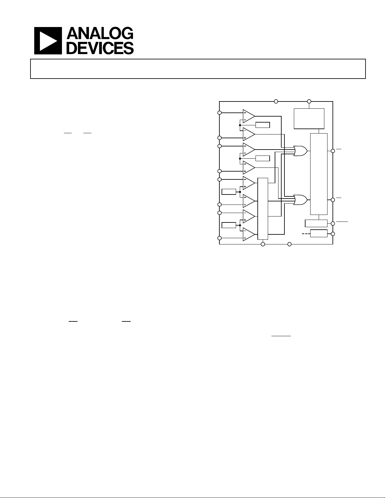
FUNCTIONAL BLOCK DIAGRAM
CC
ADM2914-EP
500mV
500mV
500mV
MUX
500mV
SEL GND
Figure 1.
TIMER
TIMER
OUTPUT
LOGIC
LOGIC
REF
UV
OV
LATCH
REF
09789-001
GENERAL DESCRIPTION
The ADM2914-EP is a quad voltage supervisory IC ideally
suited for monitoring multiple rails in a wide range of
applications.
Each monitored rail has two dedicated input pins, VHx and VLx,
which allow each rail to be monitored for both overvoltage
(OV) and undervoltage (UV) conditions. A common active low
undervoltage (
of the monitored voltage rails.
The ADM2914-EP includes a 1 V buffered reference output,
REF, that acts as an offset when monitoring a negative voltage.
The three-state SEL pin determines the polarity of the third and
fourth inputs, that is, it configures the device to monitor
positive or negative supplies.
UV
) and overvoltage (OV) pin is shared by each
The device incorporates an internal shunt regulator that enables
the device to be used in higher voltage systems. This feature
requires a resistor to be placed between the main supply rail and
the V
pin to limit the current flow into the VCC pin to no
CC
greater than 10 mA. The ADM2914-EP uses the internal shunt
regulator to regulate V
if the supply line exceeds the absolute
CC
maximum ratings.
The ADM2914-EP offers a latching overvoltage output that can
be cleared by toggling the
LATCH
input pin.
The ADM2914-EP is available in a 16-lead QSOP package. The
device operates over the extended temperature range of −55°C
to +125°C.
Additional application and technical information can be found
in the ADM2914 data sheet.
Rev. 0
Information furnished by Analog Devices is believed to be accurate and reliable. However, no
responsibility is assumed by Anal og Devices for its use, nor for any infringements of patents or ot her
rights of third parties that may result from its use. Specifications subject to change without notice. No
license is granted by implication or otherwise under any patent or patent rights of Analog Devices.
Trademarks and registered trademarks are the property of their respective owners.
One Technology Way, P.O. Box 9106, Norwood, MA 02062-9106, U.S.A.
Tel: 781.329.4700 www.analog.com
Fax: 781.461.3113 ©2011 Analog Devices, Inc. All rights reserved.
Page 2

ADM2914-EP
TABLE OF CONTENTS
Features.............................................................................................. 1
Enhanced Product Features ............................................................ 1
Applications....................................................................................... 1
Functional Block Diagram .............................................................. 1
General Description ......................................................................... 1
Revision History ............................................................................... 2
Specifications..................................................................................... 3
REVISION HISTORY
6/11—Revision 0: Initial Version
Absolute Maximum Ratings ............................................................4
ESD Caution...................................................................................4
Pin Configuration and Function Descriptions..............................5
Typical Performance Characteristics..............................................6
Outline Dimensions..........................................................................8
Ordering Guide .............................................................................8
Rev. 0 | Page 2 of 8
Page 3

ADM2914-EP
SPECIFICATIONS
/
OV
UV
/
OV
UV
LATCH
= −1 μA
= 2.5 mA
= VCC,
+ 5 mV
UOT
TA = −55°C to +125°C. Typical values at TA = 25°C, unless otherwise noted. VCC = 3.3 V, VLx = 0.45 V, VHx = 0.55 V,
SEL = V
, unless otherwise noted.
CC
Table 1.
Parameter Min Typ Max Unit Test Conditions/Comments
SHUNT REGULATOR
VCC Shunt Regulator Voltage, V
SHUNT
6.2 6.6 7.0 V TA = −55°C to +125°C
VCC Shunt Regulator Load Regulation, ΔV
SHUNT
SUPPLY
Supply Voltage, V
Minimum VCC Output Valid, V
Supply Undervoltage Lockout, V
Supply Undervoltage Lockout Hysteresis, ΔV
Supply Current, I
CC1
CCR(MIN)
CC(UVLO)
CC(HYST)
CC
REFERENCE OUTPUT
Reference Output Voltage, V
REF
0.985 1 1.020 V TA = −55°C to +125°C
UNDERVOLTAGE/OVERVOLTAGE CHARACTERISTICS
Undervoltage/Overvoltage Threshold, V
Undervoltage/Overvoltage Threshold to Output Delay, t
VHx, VLx Input Current, I
VHL
UOT
UOD
±30 nA TA = −55°C to +125°C
UV
/OV Timeout Period, t
UOTO
6 8.5 14 ms TA = −55°C to +125°C
OV
LATCH CLEAR INPUT
OV
Latch Clear Threshold Input High, V
OV
Latch Clear Threshold Input Low, V
LATCH
Input Current, I
LATCH
LATCH
LATCH
(IH)
(IL)
TIMER CHARACTERISTICS
TIMER Pull-Up Current, I
TIMER(UP)
−1.2 −2.1 −2.8 μA TA = −55°C to +125°C
TIMER Pull-Down Current, I
TIMER(DOWN)
1.2 2.1 2.8 μA TA = −55°C to +125°C
TIMER Disable Voltage, V
TIMER(DIS)
OUTPUT VOLTAGE
Output Voltage High, UV/OV, V
Output Voltage Low, UV/OV, V
OH
OL
0.01 0.15 V
THREE-STATE INPUT SEL
Low Level Input Voltage, VIL 0.4 V
High Level Input Voltage, VIH 1.4 V
Pin Voltage When Left in High-Z State, V
Z
0.6 0.9 1.2 V TA = −55°C to +125°C
SEL High, Low Input Current, I
Maximum SEL Input Current, I
1
The maximum voltage on the VCC pin is limited by the input current. The VCC pin has an internal 6.5 V shunt regulator and, therefore, a low impedance supply greater
than 6 V may exceed the maximum allowed input current. When operating from a higher supply than 6 V, always use a dropper resistor.
SEL
SEL(MAX)
6.2 6.6 6.9 V ICC = 5 mA
200 300 mV ICC = 2 mA to 10 mA
2.3 V
V
SHUNT
1 V
1.9 2 2.1 V VCC rising
5 25 50 mV
62 100 μA VCC = 2.3 V to 6 V
0.985 1 1.015 V I
= ±1 mA
VREF
492.5 500 507.5 mV
50 125 500 μs VHx = V
− 5 mV or VLx = V
UOT
±15 nA
6 8.5 12.5 ms C
TIMER
= 1 nF
1.2 V
0.8 V
> 0.5 V
±1 μA
−1.3 −2.1 −2.8 μA V
1.3 2.1 2.8 μA V
V
LATCH
TIMER
TIMER
= 0 V
= 1.6 V
−180 −270 mV Referenced to VCC
= 2.3 V; I
1 V
0.1 0.3 V
0.7 0.9 1.1 V I
V
CC
= 2.3 V; I
V
CC
= 1 V; IUV = 100 μA
V
CC
= ±10 μA
SEL
±25 μA
±30 μA SEL tied to VCC or GND
Rev. 0 | Page 3 of 8
Page 4

ADM2914-EP
ABSOLUTE MAXIMUM RATINGS
Table 2.
Parameter Rating
VCC −0.3 V to +6 V
UV, OV
TIMER −0.3 V to (VCC + 0.3 V)
VLx, VHx, LATCH, SEL
ICC 10 mA
Reference Load Current (I
IUV, IOV 10 mA
Storage Temperature Range −65°C to +150°C
Operating Temperature Range −55°C to +125°C
Lead Temperature (Soldering, 10 sec) 300°C
Stresses above those listed under Absolute Maximum Ratings
may cause permanent damage to the device. This is a stress
rating only; functional operation of the device at these or any
other conditions above those indicated in the operational
section of this specification is not implied. Exposure to absolute
maximum rating conditions for extended periods may affect
device reliability.
) ±1 mA
REF
−0.3 V to +16 V
−0.3 V to +7.5 V
Table 3. Thermal Resistance
Package Type θJA Unit
16-Lead QSOP 104 °C/W
ESD CAUTION
Rev. 0 | Page 4 of 8
Page 5

ADM2914-EP
PIN CONFIGURATION AND FUNCTION DESCRIPTIONS
V
16
CC
15
TIMER
SEL
14
13
LATCH
UV
12
11
OV
REF
10
GND
9
when not in use.
CC
09789-002
when not in use.
CC
to be latched
is held low for an adjustable timeout period set
Table 4. Pin Function Descriptions
Pin No. Mnemonic Description
1 VH1
3 VH2
2 VL1
4 VL2
5 VH3
7 VH4
Voltage High Input 1 and Voltage High Input 2. If the voltage monitored by VH1 or VH2 drops below 0.5 V, an
undervoltage condition is detected. Connect to V
Voltage Low Input 1 and Voltage Low Input 2. If the voltage monitored by VL1 or VL2 rises above 0.5 V, an
overvoltage condition is detected. Tie to GND when not in use.
Voltage High Input 3 and Voltage High Input 4. The polarity of these inputs is determined by the state of the SEL
pin. When the monitored input is configured as a positive voltage and the voltage monitored by VH3 or VH4 drops
below 0.5 V, an undervoltage condition is detected. Conversely, when the input is configured as a negative voltage
and the input drops below 0.5 V, an overvoltage condition is detected. Connect to V
6 VL3
8 VL4
Voltage Low Input 3 and Voltage Low Input 4. The polarity of these inputs is determined by the state of the SEL pin.
When the monitored input is configured as a positive voltage and the voltage monitored by VL3 or VL4 rises above
0.5 V, an overvoltage condition is detected. Conversely, when the input is configured as a negative voltage and the
input rises above 0.5 V, an undervoltage condition is detected. Tie to GND when not in use.
9 GND Device Ground.
10 REF
Buffered Reference Output. This pin is a 1 V reference that is used as an offset when monitoring negative voltages.
This pin can source or sink 1 mA and drive loads up to 1 nF. Larger capacitive loads may lead to instability. Leave
unconnected when not in use.
11
OV
Overvoltage Reset Output. OV
threshold or if a positive polarity input voltage exceeds its threshold. The ADM2914-EP allows OV
low. This pin has a weak pull-up to VCC and can be pulled up to 16 V externally. Leave this pin unconnected when
not in use.
12
UV
Undervoltage Reset Output. UV
or if a positive polarity input voltage drops below its threshold. UV
by the external capacitor tied to the TIMER pin. The UV pin has a weak pull-up to VCC and can be pulled up to 16 V
externally via an external pull-up resistor. Leave this pin unconnected when not in use.
13
LATCH
OV
Latch Bypass Input/Clear Pin. When pulled high, the OV latch is cleared. When held high, the OV output has the
same delay and output characteristics as the UV output. When pulled low, the OV output is latched when asserted.
14 SEL
15 TIMER
Input Polarity Select. This three-state input pin allows the polarity of VH3, VL3, VH4, and VL4 to be configured.
Connect to V
or GND, or leave open to select one of three possible input polarity configurations.
CC
Adjustable Reset Delay Timer. Connect an external capacitor to the TIMER pin to program the reset timeout delay.
Refer to Figure 14 in the Typical Performance Characteristics section. Connect this pin to VCC to bypass the timer.
16 VCC
Supply Voltage. V
operates as a direct supply for voltages up to 6 V. For voltages greater than 6 V, it operates as a
CC
shunt regulator. A dropper resistor must be used in this configuration to limit the current to less than 10 mA. When
used without the resistor, the voltage at this pin must not exceed 6 V. A 0.1 μF bypass capacitor or greater should
be used.
1
VH1
VL1
2
3
VH2
ADM2914-EP
VL2
4
TOP VIEW
5
VH3
VL3
VH4
VL4
(Not to Scale)
6
7
8
Figure 2. ADM2914-EP Pin Configuration
is asserted low if a negative polarity input voltage drops below its associated
is asserted low if a negative polarity input voltage exceeds its associated threshold
Rev. 0 | Page 5 of 8
Page 6

ADM2914-EP
V
TYPICAL PERFORMANCE CHARACTERISTICS
0.505
0.504
0.503
(V)
UOT
0.502
0.501
0.500
0.499
0.498
0.497
THRESHOLD VOLTAGE,
0.496
0.495
–40 –25 –10 1251109580655035205
TEMPERATURE (°C)
Figure 3. Input Threshold Voltage vs. Temperature
09789-003
6.80
6.75
6.70
6.65
(V)
6.60
CC
V
6.55
6.50
6.45
6.40
024681
–40°C
Figure 6. V
+85°C
I
(mA)
CC
Shunt Voltage vs. ICC
CC
+25°C
0
09789-006
90
85
80
75
70
(µA)
CC
I
65
60
55
50
–40 –25 –10 1251109580655035205
6.80
6.75
6.70
6.65
(V)
6.60
CC
V
6.55
6.50
6.45
6.40
–40 –25 –10 1251109580655035205
VCC = 6V
= 3.3V
V
CC
= 2.3V
V
CC
TEMPERATURE (°C)
Figure 4. Supply Current vs. Temperature
TEMPERATURE (°C)
Figure 5. V
Shunt Voltage vs. Temperature
CC
200µA
1mA
2mA
5mA
10mA
1.020
1.015
(V)
1.010
REF
1.005
1.000
0.995
0.990
REFERENCE VO LTAGE, V
0.985
0.980
–40 –25 –10 1251109580655035205
09789-004
TEMPERATURE (°C)
09789-007
Figure 7. Buffered Reference Voltage vs. Temperature
1000
900
800
700
600
500
400
300
TRANSIENT DURATI ON (µs)
200
100
0
09789-005
0.1 1 10 100
VCC = 6V
VCC = 2.3V
COMPARATOR O VERDRIVE (% OF V
RESET ASSERTED
ABOVE THE LI NE
)
TH
09789-008
Figure 8. Transient Duration vs. Comparator Overdrive
Rev. 0 | Page 6 of 8
Page 7

ADM2914-EP
14
13
(ms)
12
UOTO
t
11
3.0
2.5
(mA)
2.0
UV
1.5
VHx = 0.45V
SEL = V
CC
UV = 150mV
10
9
8
UV/OV TIMEOUT PERIOD,
7
–40 –25 –10 1251109580655035205
Figure 9.
0.9
0.8
0.7
0.6
0.5
0.4
0.3
UV VOLTAGE (V)
0.2
0.1
0
–0.1
0 0. 1 0.2 0.3 0.4 0.5 0.6 0.7 0.8 0.9 1.0
Figure 10.
TEMPERATURE (°C)
UV
/OV Timeout Period vs. Temperature
WITH 10kΩ PULL-UP
WITHOUT PULL-UP
SUPPLY VOLTAGE, V
UV
Output Voltage vs. VCC
(V)
CC
1.0
SINK
–40°C
SINK
UV = 50mV
CC
, IUV vs. VCC
(mA)
(V)
+25°C
09789-012
09789-013
0.5
PULL-DOW N CURRENT I
0
–0.5
012 3456
09789-009
SUPPLY VOLTAGE, V
Figure 12. I
1000
900
800
700
600
(mV)
OL
500
400
UV/OV, V
300
200
100
0
0 5 10 15
09789-010
Figure 13.
UV
+85°C
I
/OV Voltage Output Low vs. Output Sink Current
5.0
VHx = 0.55V
4.5
SEL = V
CC
4.0
3.5
3.0
2.5
2.0
UV VOLTAGE (V)
1.5
1.0
0.5
0
01234
SUPPLY VOLTAGE, V
Figure 11.
UV
Output Voltage vs. VCC
(V)
CC
5
09789-011
10k
(ms)
1k
UOTO
t
100
10
UV/OV TIMEOUT PERIOD,
1
0.1 1 10 100 1000
TIMER PIN CAPACITANCE C
Figure 14.
UV
/OV Timeout Period vs. Capacitance
TIMER
(nF)
09789-014
Rev. 0 | Page 7 of 8
Page 8

ADM2914-EP
OUTLINE DIMENSIONS
0.197 (5.00)
0.193 (4.90)
0.189 (4.80)
16
1
0.065 (1.65)
0.049 (1.25)
0.010 (0.25)
0.004 (0.10)
COPLANARITY
0.004 (0.10)
0.025 (0.64)
BSC
CONTROLLING DIMENSIONS ARE IN INCHES; MILLIMETER DIMENSIONS
(IN PARENTHESES) ARE ROUNDED-OFF INCH EQUIVALENTS FOR
REFERENCE ONLY AND ARE NOT APPROPRIATE FOR USE IN DESIGN.
Figure 15. 16-Lead Shrink Small Outline Package [QSOP]
ORDERING GUIDE
Model1 Temperature Range Package Description Package Option
ADM2914-1SRQZEP −55°C to +125°C 16-Lead Shrink Small Outline Package [QSOP] RQ-16
ADM2914-1SRQZEP-R7 −55°C to +125°C 16-Lead Shrink Small Outline Package [QSOP] RQ-16
1
Z = RoHS Compliant Part.
9
0.158 (4.01)
0.154 (3.91)
0.150 (3.81)
8
0.069 (1.75)
0.053 (1.35)
SEATING
0.012 (0.30)
0.008 (0.20)
COMPLIANT TO JEDEC STANDARDS MO-137-AB
PLANE
0.244 (6.20)
0.236 (5.99)
0.228 (5.79)
8°
0°
0.010 (0.25)
0.006 (0.15)
(RQ-16)
Dimensions shown in inches and (millimeters)
0.050 (1.27)
0.016 (0.41)
0.020 (0.51)
0.010 (0.25)
0.041 (1.04)
REF
01-28-2008-A
©2011 Analog Devices, Inc. All rights reserved. Trademarks and
registered trademarks are the property of their respective owners.
D09789-0-6/11(0)
Rev. 0 | Page 8 of 8
 Loading...