

5 kV rms Signal and Power Isolated
V
V
RS-485 Transceiver with ±15 kV ESD
FEATURES
5 kV rms isolated RS-485/RS-422 transceiver, configurable as
half or full duplex
isoPower integrated isolated dc-to-dc converter
±15 kV ESD protection on RS-485 input/output pins
Complies with ANSI/TIA/EIA-485-A-98 and ISO 8482:1987(E)
Data rate: 16 Mbps (ADM2682E), 500 kbps (ADM2687E)
5 V or 3.3 V operation
Connect up to 256 nodes on one bus
Open- and short-circuit, fail-safe receiver inputs
High common-mode transient immunity: >25 kV/μs
Thermal shutdown protection
Safety and regulatory approvals
UL recognition (pending)
5000 V rms for 1 minute per UL 1577
CSA Component Acceptance Notice #5A (pending)
IEC 60601-1: 400 V rms (basic), 250 V rms (reinforced)
IEC 60950-1: 600 V rms (basic), 380 V rms (reinforced)
VDE Certificates of Conformity (pending)
DIN EN 60747-5-2 (VDE 0884 Part 2): 2003-01
V
= 846 V peak
IORM
Operating temperature range: −40°C to +85°C
16-lead wide-body SOIC with >8 mm creepage and clearance
APPLICATIONS
Isolated RS-485/RS-422 interfaces
Industrial field networks
Multipoint data transmission systems
CC
DIGITAL ISOLATION iCou pler
TxD
DE
RxD
RE
ADM2682E/ADM2687E
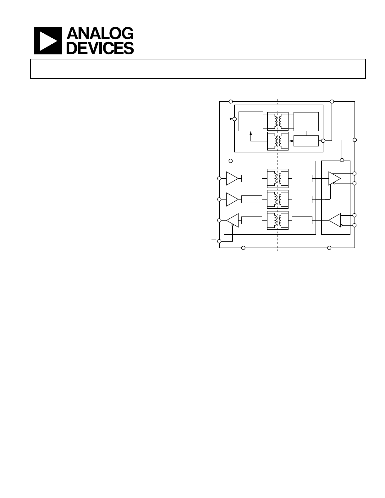
FUNCTIONAL BLOCK DIAGRAM
ISOOUT
isoPower DC-TO-DC CONVERTER
OSCILLATOR
ENCODE
ENCODE
DECODE
GND
1
ISOLATION
BARRIER
Figure 1.
RECTIFIER
REGULATOR
TRANSCEIVER
DECODE D
DECODE
ENCODE
ADM2682E/ADM2687E
GND
V
ISOIN
Y
Z
R
2
A
B
09927-001
GENERAL DESCRIPTION
The ADM2682E/ADM2687E are fully integrated 5 kV rms
signal and power isolated data transceivers with ±15 kV ESD
protection and are suitable for high speed communication on
multipoint transmission lines. The ADM2682E/ADM2687E
include an integrated 5 kV rms isolated dc-to-dc power supply
that eliminates the need for an external dc-to-dc isolation block.
They are designed for balanced transmission lines and comply
with ANSI/TIA/EIA-485-A-98 and ISO 8482:1987(E).
The devices integrate Analog Devices, Inc., iCoupler® technology to
combine a 3-channel isolator, a three-state differential line driver, a
differential input receiver, and Analog Devices isoPower® dc-to-dc
converter into a single package. The devices are powered by a
single 5 V or 3.3 V supply, realizing a fully integrated signal and
power isolated RS-485 solution.
Rev. 0
Information furnished by Analog Devices is believed to be accurate and reliable. However, no
responsibility is assumed by Analog Devices for its use, nor for any infringements of patents or other
rights of third parties that may result from its use. Specifications subject to change without notice. No
license is granted by implication or otherwise under any patent or patent rights of Analog Devices.
Trademarks and registered trademarks are the property of their respective owners.
The ADM2682E/ADM2687E drivers have an active high enable.
An active low receiver enable is also provided, which causes the
receiver output to enter a high impedance state when disabled.
The devices have current limiting and thermal shutdown
features to protect against output short circuits and situations
where bus contention may cause excessive power dissipation.
The parts are fully specified over the industrial temperature
range and are available in a highly integrated, 16-lead, widebody SOIC package with >8 mm creepage and clearance.
The ADM2682E/ADM2687E contain isoPower technology that
uses high frequency switching elements to transfer power through
the transformer. Special care must be taken during printed circuit
board (PCB) layout to meet emissions standards. Refer to
AN-0971 Application Note, Recommendations for Control of
Radiated Emissions with isoPower Devices, for details on board
layout considerations.
One Technology Way, P.O. Box 9106, Norwood, MA 02062-9106, U.S.A.
Tel: 781.329.4700 www.analog.com
Fax: 781.461.3113 ©2011 Analog Devices, Inc. All rights reserved.

ADM2682E/ADM2687E
TABLE OF CONTENTS
Features.............................................................................................. 1
Applications....................................................................................... 1
Functional Block Diagram .............................................................. 1
General Description ......................................................................... 1
Revision History ............................................................................... 2
Specifications..................................................................................... 3
ADM2682E Timing Specifications ............................................ 4
ADM2687E Timing Specifications ............................................ 4
Package Characteristics ............................................................... 4
Regulatory Information............................................................... 5
Insulation and Safety-Related Specifications............................ 5
VDE 0884 Insulation Characteristics (Pending)...................... 6
Absolute Maximum Ratings............................................................ 7
ESD Caution.................................................................................. 7
Pin Configuration and Function Descriptions............................. 8
Typical Performance Characteristics ............................................. 9
Test Circuits..................................................................................... 14
Switching Characteristics .............................................................. 15
Circuit Description......................................................................... 16
Signal Isolation ........................................................................... 16
Power Isolation ........................................................................... 16
Truth Tables................................................................................. 16
Thermal Shutdown .................................................................... 16
Open- and Short-Circuit, Fail-Safe Receiver Inputs.............. 16
DC Correctness and Magnetic Field Immunity........................... 16
Applications Information.............................................................. 18
PCB Layout ................................................................................. 18
EMI Considerations................................................................... 18
Insulation Lifetime..................................................................... 19
Isolated Supply Considerations................................................ 19
Typical Applications................................................................... 20
Outline Dimensions....................................................................... 22
Ordering Guide .......................................................................... 22
REVISION HISTORY
7/11—Revision 0: Initial Version
Rev. 0 | Page 2 of 24
ADM2682E/ADM2687E
SPECIFICATIONS
All voltages are relative to their respective ground; 3.0 ≤ VCC ≤ 5.5 V. All minimum/maximum specifications apply over the entire
recommended operation range, unless otherwise noted. All typical specifications are at T
Table 1.
Parameter Symbol Min Typ Max Unit Test Conditions/Comments
ADM2687E SUPPLY CURRENT ICC
Data Rate ≤ 500 kbps 90 mA VCC = 3.3 V, 100 Ω load between Y and Z
72 mA VCC = 5 V, 100 Ω load between Y and Z
125 mA VCC = 3.3 V, 54 Ω load between Y and Z
98 mA VCC = 5 V, 54 Ω load between Y and Z
140 mA 120 Ω load between Y and Z
ADM2682E SUPPLY CURRENT ICC
Data Rate = 16 Mbps 175 mA 120 Ω load between Y and Z
260 mA 54 Ω load between Y and Z
Data Rate = 16 Mbps, 4.5 ≤ VCC ≤ 5.5 V 130 mA 120 Ω load between Y and Z
200 mA 54 Ω load between Y and Z
ISOLATED SUPPLY VOLTAGE V
3.3 V
ISOOUT
DRIVER
Differential Outputs
Differential Output Voltage, Loaded |V
| 2.0 3.6 V RL = 100 Ω (RS-422), see Figure 29
OD2
1.5 3.6 V RL = 54 Ω (RS-485), see Figure 29
|V
| 1.5 3.6 V −7 V ≤ V
OD3
Δ|VOD| for Complementary Output States Δ|VOD| 0.2 V RL = 54 Ω or 100 Ω, see Figure 29
Common-Mode Output Voltage VOC 3.0 V RL = 54 Ω or 100 Ω, see Figure 29
Δ|VOC| for Complementary Output States Δ|VOC| 0.2 V RL = 54 Ω or 100 Ω, see Figure 29
Short-Circuit Output Current IOS 200 mA
Output Leakage Current (Y, Z) IO 30 μA
−30 μA
Logic Inputs DE, RE, TxD
Input Threshold Low VIL 0.27 VCC V
Input Threshold High VIH 0.7 VCC V
Input Current II −10 0.01 10 μA
RECEIVER
Differential Inputs
Differential Input Threshold Voltage VTH −200 −125 −30 mV −7 V < VCM < +12 V
Input Voltage Hysteresis V
15 mV VOC = 0 V
HYS
Input Current (A, B) II 125 μA DE = 0 V, VCC = 0 V or 3.6 V, VIN = 12 V
−100 μA DE = 0 V, VCC = 0 V or 3.6 V, VIN = −7 V
Line Input Resistance RIN 96 kΩ −7 V < VCM < +12 V
Logic Outputs
Output Voltage Low VOL 0.2 0.4 V IO = 1.5 mA, VA − VB = −0.2 V
Output Voltage High VOH V
− 0.3 VCC − 0.2 V IO = −1.5 mA, VA − VB = 0.2 V
CC
Short-Circuit Current 100 mA
COMMON-MODE TRANSIENT IMMUNITY1 25 kV/μs VCM = 1 kV, transient magnitude = 800 V
1
CM is the maximum common-mode voltage slew rate that can be sustained while maintaining specification-compliant operation. VCM is the common-mode potential
difference between the logic and bus sides. The transient magnitude is the range over which the common-mode is slewed. The common-mode voltage slew rates
apply to both rising and falling common-mode voltage edges.
= 25°C, VCC = 5 V unless otherwise noted.
A
≤ 12 V, see Figure 30
TEST1
DE = 0 V, RE
= 0 V, VCC = 0 V or 3.6 V,
VIN = 12 V
DE = 0 V, RE
= 0 V, VCC = 0 V or 3.6 V,
VIN = −7 V
, TxD
DE, RE
, TxD
DE, RE
, TxD
DE, RE
Rev. 0 | Page 3 of 24

ADM2682E/ADM2687E
ADM2682E TIMING SPECIFICATIONS
TA = −40°C to +85°C.
Table 2.
Parameter Symbol Min Typ Max Unit Test Conditions/Comments
DRIVER
Maximum Data Rate 16 Mbps
Propagation Delay, Low to High t
Propagation Delay, High to Low t
Output Skew t
Rise Time/Fall Time tDR, tDF 15 ns RL = 54 Ω, CL1 = CL2 = 100 pF, see Figure 31 and Figure 35
Enable Time tZL, tZH 120 ns RL = 110 Ω, CL = 50 pF, see Figure 32 and Figure 37
Disable Time tLZ, tHZ 150 ns RL = 110 Ω, CL = 50 pF, see Figure 32 and Figure 37
RECEIVER
Propagation Delay, Low to High t
Propagation Delay, High to Low t
Output Skew1 t
Enable Time tZL, tZH 15 ns RL = 1 kΩ, CL = 15 pF, see Figure 34 and Figure 38
Disable Time tLZ, tHZ 15 ns RL = 1 kΩ, CL = 15 pF, see Figure 34 and Figure 38
1
Guaranteed by design.
ADM2687E TIMING SPECIFICATIONS
TA = −40°C to +85°C.
Table 3.
Parameter Symbol Min Typ Max Unit Test Conditions/Comments
DRIVER
Maximum Data Rate 500 kbps
Propagation Delay, Low to High t
Propagation Delay, High to Low t
Output Skew t
Rise Time/Fall Time tDR, tDF 200 1100 ns RL = 54 Ω, CL1 = CL2 = 100 pF, see Figure 31 and Figure 35
Enable Time tZL, tZH 2.5 μs RL = 110 Ω, CL = 50 pF, see Figure 32 and Figure 37
Disable Time tLZ, tHZ 200 ns RL = 110 Ω, CL = 50 pF, see Figure 32 and Figure 37
RECEIVER
Propagation Delay, Low to High t
Propagation Delay, High to Low t
Output Skew t
Enable Time tZL, tZH 15 ns RL = 1 kΩ, CL = 15 pF, see Figure 34 and Figure 38
Disable Time tLZ, tHZ 15 ns RL = 1 kΩ, CL = 15 pF, see Figure 34 and Figure 38
63 100 ns RL = 54 Ω, CL1 = C
DPLH
64 100 ns RL = 54 Ω, CL1 = C
DPHL
1 8 ns RL = 54 Ω, CL1 = CL2 = 100 pF, see Figure 31 and Figure 35
SKEW
94 110 ns CL = 15 pF, see Figure 33 and Figure 36
RPLH
95 110 ns CL = 15 pF, see Figure 33 and Figure 36
RPHL
1 12 ns CL = 15 pF, see Figure 33 and Figure 36
SKEW
250 503 700 ns RL = 54 Ω, CL1 = C
DPLH
250 510 700 ns RL = 54 Ω, CL1 = C
DPHL
7 100 ns RL = 54 Ω, CL1 = CL2 = 100 pF, see Figure 31 and Figure 35
SKEW
91 200 ns CL = 15 pF, see Figure 33 and Figure 36
RPLH
95 200 ns CL = 15 pF, see Figure 33 and Figure 36
RPHL
4 30 ns CL = 15 pF, see Figure 33 and Figure 36
SKEW
= 100 pF, see Figure 31 and Figure 35
L2
= 100 pF, see Figure 31 and Figure 35
L2
= 100 pF, see Figure 31 and Figure 35
L2
= 100 pF, see Figure 31 and Figure 35
L2
PACKAGE CHARACTERISTICS
Table 4.
Parameter Symbol Min Typ Max Unit Test Conditions/Comments
Resistance (Input-to-Output)1 R
Capacitance (Input-to-Output)1 C
Input Capacitance2 C
1
Device considered a 2-terminal device: short together Pin 1 to Pin 8 and short together Pin 9 to Pin 16.
2
Input capacitance is from any input data pin to ground.
10
I-O
3 pF f = 1 MHz
I-O
4 pF
I
Rev. 0 | Page 4 of 24
12
Ω

ADM2682E/ADM2687E
REGULATORY INFORMATION
Table 5. ADM2682E/ADM2687E Approvals (Pending)
Organization Approval Type
UL (Pending)
CSA (Pending)
VDE (Pending)
INSULATION AND SAFETY-RELATED SPECIFICATIONS
Table 6.
Parameter Symbol Value Unit Test Conditions/Comments
Rated Dielectric Insulation Voltage 5000 V rms 1-minute duration
Minimum External Air Gap (Clearance) L(I01) >8.0 mm
Minimum External Tracking (Creepage) L(I02) >8.0 mm
Minimum Internal Gap (Internal Clearance) 0.017 min mm Insulation distance through insulation
Tracking Resistance (Comparative Tracking Index) CTI >175 V DIN IEC 112/VDE 0303-1
Isolation Group IIIa Material Group (DIN VDE 0110:1989-01, Table 1)
To be recognized under the UL 1577 Component Recognition Program of Underwriters Laboratories, Inc.
Single protection, 5000 V rms isolation voltage.
In accordance with UL 1577, each ADM2682E/ADM2687E is proof tested by applying an insulation test voltage
≥ 6000 V rms for 1 second.
To be approved under CSA Component Acceptance Notice #5A.
Reinforced insulation per IEC 60601-1, 250 V rms (353 V peak) maximum working voltage.
Basic insulation per IEC 60601-1, 400 V rms (566 V peak) maximum working voltage.
Reinforced insulation per CSA 60950-1-07 and IEC 60950-1, 380 V rms (537 V peak) maximum working voltage.
Basic insulation per CSA 60950-1-07 and IEC 60950-1, 600 V rms (848 V peak) maximum working voltage.
To be certified according to DIN EN 60747-5-2 (VDE 0884 Part 2):2003-01.
In accordance with DIN EN 60747-5-2, each ADM2682E/ADM2687E is proof tested by applying an insulation test voltage
≥1590 V peak for 1 second.
Measured from input terminals to output terminals,
shortest distance through air
Measured from input terminals to output terminals,
shortest distance along body
Rev. 0 | Page 5 of 24

ADM2682E/ADM2687E
VDE 0884 INSULATION CHARACTERISTICS (PENDING)
This isolator is suitable for basic electrical isolation only within the safety limit data. Maintenance of the safety data must be ensured by
means of protective circuits.
Table 7.
Description Test Conditions/Comments Symbol Characteristic Unit
CLASSIFICATIONS
Installation Classification per DIN VDE 0110 for
Rated Mains Voltage
≤300 V rms I to IV
≤450 V rms I to III
≤600 V rms I to II
Climatic Classification 40/85/21
Pollution Degree Table 1 of DIN VDE 0110 2
VOLTAGE
Maximum Working Insulation Voltage V
Input-to-Output Test Voltage VPR
Method b1
Method a
After Environmental Tests, Subgroup 1 V
After Input and/or Safety Test,
Subgroup 2/Subgroup 3
Highest Allowable Overvoltage Transient overvoltage, tTR = 10 sec VTR 6000 V peak
SAFETY-LIMITING VALUES Maximum value allowed in the event of a failure
Case Temperature TS 150 °C
Input Current I
Output Current I
Insulation Resistance at TS V
846 V peak
IORM
× 1.875 = VPR, 100% production tested,
V
IORM
= 1 sec, partial discharge < 5 pC
t
m
× 1.6 = VPR, tm = 60 sec, partial discharge < 5 pC 1375 V peak
IORM
× 1.2 = VPR, tm = 60 sec, partial discharge < 5 pC 1018 V peak
V
IORM
= 500 V RS >109 Ω
IO
1590 V peak
265 mA
S, INPUT
335 mA
S, OUTPUT
Rev. 0 | Page 6 of 24
ADM2682E/ADM2687E
ABSOLUTE MAXIMUM RATINGS
TA = 25°C, unless otherwise noted. All voltages are relative to
their respective ground.
Table 8.
Parameter Rating
VCC −0.5 V to +7 V
Digital Input Voltage (DE, RE, TxD)
Digital Output Voltage (RxD) −0.5 V to VDD + 0.5 V
Driver Output/Receiver Input Voltage −9 V to +14 V
Operating Temperature Range −40°C to +85°C
Storage Temperature Range −55°C to +150°C
ESD (Human Body Model) on
A, B, Y, and Z pins
ESD (Human Body Model) on Other Pins
Thermal Resistance θJA
Lead Temperature
Soldering (10 sec) 260°C
Vapor Phase (60 sec) 215°C
Infrared (15 sec) 220°C
−0.5 V to V
±15 kV
±2 kV
52°C/W
+ 0.5 V
DD
Stresses above those listed under Absolute Maximum Ratings
may cause permanent damage to the device. This is a stress
rating only; functional operation of the device at these or any
other conditions above those indicated in the operational
section of this specification is not implied. Exposure to absolute
maximum rating conditions for extended periods may affect
device reliability.
Table 9. Maximum Continuous Working Voltage
Parameter Max Unit Reference Standard
AC Voltage
Bipolar Waveform 424 V peak
Unipolar Waveform
Basic Insulation 600 V peak
Reinforced Insulation 537 V peak
DC Voltage
Basic Insulation 600 V peak
Reinforced Insulation 537 V peak
1
Refers to continuous voltage magnitude imposed across the isolation
barrier. See the Insulation Lifetime section for more details.
ESD CAUTION
1
All certifications,
50-year minimum
lifetime
Maximum approved
working voltage per
IEC 60950-1
Maximum approved
working voltage per
IEC 60950-1
Rev. 0 | Page 7 of 24
ADM2682E/ADM2687E
PIN CONFIGURATION AND FUNCTION DESCRIPTIONS
1
GND
1
V
2
CC
3
RxD
TxD
V
GND
NOTES
1. PIN 10 AND PIN 15 M UST BE
CONNECTED EXT ERNALLY.
RE
DE
CC
1
ADM2682E/
4
ADM2687E
5
TOP VIEW
(Not to Scale)
6
7
8
16
GND
2
V
15
ISOIN
14
A
B
13
12
Z
Y
11
10
V
ISOOUT
GND
9
2
09927-002
Figure 2. Pin Configuration
Table 10. Pin Function Descriptions
Pin No. Mnemonic Description
1 GND1 Ground, Logic Side.
2 V
CC
Logic Side Power Supply. It is recommended that a 0.1 μF and a 0.01 μF decoupling capacitor be fitted between
Pin 2 and Pin 1.
3 RxD
4
Receiver Enable Input. This is an active-low input. Driving this input low enables the receiver, while driving it high
RE
Receiver Output Data. This output is high when (A − B) ≥ −30 mV and low when (A − B) ≤ –200 mV. The output is
tristated when the receiver is disabled, that is, when RE
is driven high.
disables the receiver.
5 DE Driver Enable Input. Driving this input high enables the driver, while driving it low disables the driver.
6 TxD Driver Input. Data to be transmitted by the driver is applied to this input.
7 V
CC
Logic Side Power Supply. It is recommended that a 0.1 μF and a 10 μF decoupling capacitor be fitted between
Pin 7 and Pin 8.
8 GND1 Ground, Logic Side.
9 GND2 Ground, Bus Side.
10 V
ISOOUT
Isolated Power Supply Output. This pin must be connected externally to V
. It is recommended that a reservoir
ISOIN
capacitor of 10 μF and a decoupling capacitor of 0.1 μF be fitted between Pin 10 and Pin 9.
11 Y Driver Noninverting Output
12 Z Driver Inverting Output
13 B Receiver Inverting Input.
14 A Receiver Noninverting Input.
15 V
ISOIN
Isolated Power Supply Input. This pin must be connected externally to V
. It is recommended that a 0.1 μF
ISOOUT
and a 0.01 μF decoupling capacitor be fitted between Pin 15 and Pin 16.
16 GND2 Ground, Bus Side.
Rev. 0 | Page 8 of 24

ADM2682E/ADM2687E
TYPICAL PERFORMANCE CHARACTERISTICS
200
180
160
140
(mA)
CC
120
100
80
60
SUPPLY CURRENT, I
40
20
0
–40 –15 10 35 60 85
Figure 3. ADM2682E Supply Current (I
(Data Rate = 16 Mbps, DE = 3.3 V, V
160
R
= 54
L
= 120
R
L
NO LOAD
TEMPERAT URE (°C)
) vs. Temperature
CC
= 3.3 V)
CC
09927-203
140
120
= 54
R
100
(mA)
CC
80
60
40
SUPPLY CURRENT, I
20
0
1 4 7 10 13 16
Figure 6. ADM2682E Supply Current (I
(T
= 25°C, DE = 5 V, VCC = 5 V)
A
120
L
= 120
R
L
NO LOAD
DATA RATE (M bps)
) vs. Data Rate
CC
09927-206
140
R
= 54
120
(mA)
CC
100
80
60
40
SUPPLY CURRENT, I
20
0
–40 –15 10 35 60 85
Figure 4. ADM2682E Supply Current (I
(Data Rate = 16 Mbps, DE = 5 V, V
180
160
140
(mA)
120
CC
100
80
60
SUPPLY CURRENT, I
40
20
0
1 4 7 10 13 16
Figure 5. ADM2682E Supply Current (I
= 25°C, DE = 3.3 V, VCC = 3.3 V)
(T
A
L
R
= 120
L
NO LOAD
TEMPERAT URE (°C)
R
= 54
L
= 120
R
L
NO LOAD
DATA RATE (M bps)
) vs. Temperature
CC
= 5 V)
CC
) vs. Data Rate
CC
100
(mA)
80
CC
60
40
SUPPLY CURRENT, I
20
0
–40 –15 10 35 60 85
09927-204
Figure 7. ADM2687E Supply Current (I
(Data Rate = 500 kbps, DE = 5 V, V
160
140
120
(mA)
CC
100
80
60
40
SUPPLY CURRENT, I
20
0
09927-205
–40 –15 10 35 60 85
Figure 8. ADM2687E Supply Current (I
(Data Rate = 500 kbps, DE = 3.3 V, V
= 54
R
L
R
= 120
L
NO LOAD
TEMPERATURE (°C)
= 54
R
L
= 120
R
L
NO LOAD
TEMPERATURE (°C)
) vs. Temperature
CC
= 5 V)
CC
) vs. Temperature
CC
= 3.3 V)
CC
09927-207
09927-208
Rev. 0 | Page 9 of 24

ADM2682E/ADM2687E
140
R
= 54
120
100
(mA)
CC
80
60
40
SUPPLY CURRENT, I
20
0
50 200125 275 350 425 500
Figure 9. ADM2687E Supply Current (I
(T
= 25°C, DE = 3.3 V, VCC = 3.3 V)
A
120
100
(mA)
80
CC
60
L
R
= 120
L
NO LOAD
DATA RATE (kbps)
= 54
R
L
R
= 120
L
) vs. Data Rate
CC
09927-209
600
580
560
540
520
500
480
460
440
DRIVER PRO PAGATI ON DELAY (ns)
420
400
–40 –15 10 35 60 85
t
DPLH
t
DPHL
TEMPERATURE (°C)
09927-108
Figure 12. ADM2687E Differential Driver Propagation Delay vs. Temperature
TxD
1
40
SUPPLY CURRENT, I
20
0
50 200125 275 350 425 500
Figure 10. ADM2687E Supply Current (I
(T
A
72
70
68
66
64
62
60
58
56
54
DRIVER PROPAGATI ON DELAY (ns)
52
50
–40 –15 10 35 60 85
t
DPHL
NO LOAD
DATA RATE (kbps)
CC
= 25°C, DE = 5 V, VCC = 5 V)
t
DPLH
TEMPERATURE (°C)
) vs. Data Rate
09927-210
09927-107
Figure 11. ADM2682E Differential Driver Propagation Delay vs. Temperature
Z
Y
3
CH1 2.0V
CH3 2.0V
CH2 2.0V
M10.00ns A CH1 1.28V
Figure 13. ADM2682E Driver Propagation Delay
1
3
CH1 2.0V
CH3 2.0V
TxD
Z
Y
CH2 2.0V M200ns A CH1 2.56V
Figure 14. ADM2687E Driver Propagation Delay
09927-109
09927-110
Rev. 0 | Page 10 of 24

ADM2682E/ADM2687E
0
0.32
–10
–20
–30
–40
–50
OUTPUT CURRENT (mA)
–60
–70
012345
OUTPUT HI GH VOLTAGE (V)
Figure 15. Receiver Output Current vs. Receiver Output High Voltage
60
50
40
30
20
OUTPUT CURRE NT (mA)
10
0.30
0.28
0.26
0.24
OUTPUT LOW VOLTAGE (V)
0.22
0.20
–40 –15 10 35 60 85
09927-111
TEMPERATURE (°C)
09927-114
Figure 18. Receiver Output Low Voltage vs. Temperature
B
1
3
A
RxD
0
012345
OUTPUT LOW VOLTAGE (V)
Figure 16. Receiver Output Current vs. Receiver Output Low Voltage
4.75
4.74
4.73
4.72
4.71
4.70
4.69
4.68
OUTPUT HIG H VOLTAG E (V)
4.67
4.66
4.65
–40 –15 10 35 60 85
TEMPERATURE (°C)
Figure 17. Receiver Output High Voltage vs. Temperature
CH1 2.0V
09927-112
CH3 2.0V
CH2 2.0V M10. 00ns A CH1 2. 56V
09927-115
Figure 19. ADM2682E Receiver Propagation Delay
A
1
3
CH1 2.0V
09927-113
CH3 2.0V
CH2 2.0V M10. 00ns A CH1 2. 56V
B
RxD
09927-116
Figure 20. ADM2687E Receiver Propagation Delay
Rev. 0 | Page 11 of 24

ADM2682E/ADM2687E
G
A
A
98
97
Y (ns)
96
t
TION DEL
95
94
93
RECEIVER PRO PA
92
–40 –15 10 35 60 85
TEMPERATURE (°C)
RPHL
t
RPLH
Figure 21. ADM2682E Receiver Propagation Delay vs. Temperature
100
99
98
97
96
95
94
93
92
RECEIVER PROPAGATI ON DELAY (ns)
91
90
–40 –15 10 35 60 85
t
RPHL
t
RPLH
TEMPERATURE (°C)
Figure 22. ADM2687E Receiver Propagation Delay vs. Temperature
3.39
3.44
3.43
3.42
3.41
3.40
3.39
3.38
3.37
3.36
ISOLATED SUPPLY VOLTAGE (V)
3.35
3.34
09927-117
–40 10–15 35 60 85
RL = 120
NO LOAD
= 54
R
L
TEMPERATURE (°C)
09927-224
Figure 24. ADM2682E Isolated Supply Voltage vs. Temperature
= 5 V, Data Rate = 16 Mbps)
(V
CC
3.37
3.36
3.35
3.34
3.33
3.32
ISOLATED SUPPLY VOLTAGE (V)
3.31
3.30
–40 10–15 35 60 85
09927-118
RL = 120
NO LOAD
= 54
R
L
TEMPERATURE (°C)
09927-225
Figure 25. ADM2687E Isolated Supply Voltage vs. Temperature
(V
= 3.3 V, Data Rate = 500 kbps)
CC
3.39
3.38
NO LOAD
ISOLATED SUPPLY VOLT AGE (V)
3.37
3.36
3.35
3.34
3.33
RL = 120
= 54
R
L
–40 10–15 35 60 85
TEMPERATURE (°C)
Figure 23. ADM2682E Isolated Supply Voltage vs. Temperature
= 3.3 V, Data Rate = 16 Mbps)
(V
CC
09927-223
3.38
3.37
3.36
3.35
3.34
3.33
ISOLATED SUPPLY VOLTAGE (V)
3.32
3.31
–40 10–15 35 60 85
RL = 120
NO LOAD
R
= 54
L
TEMPERATURE (°C)
Figure 26. ADM2687E Isolated Supply Voltage vs. Temperature
= 5 V, Data Rate = 500 kbps
(V
CC
09927-226
Rev. 0 | Page 12 of 24

ADM2682E/ADM2687E
60
R
= 54
50
40
30
L
R
L
= 120
40
35
30
25
20
R
L
R
= 120
L
= 54
20
10
ISOLATED SUPPLY CURRENT (mA)
0
–40 –15 10 35 60 85
NO LOAD
TEMPERATURE (°C)
Figure 27. ADM2682E Isolated Supply Current vs. Temperature
(V
= 3.3 V, Data Rate = 16 Mbps)
CC
15
10
ISOLATED SUPPLY CURRENT (mA)
5
0
–40 –15 10 35 60 85
09927-227
NO LOAD
TEMPERATURE (°C)
09927-228
Figure 28. ADM2687E Isolated Supply Current vs. Temperature
(VCC = 3.3 V, Data Rate = 500 kbps)
Rev. 0 | Page 13 of 24

ADM2682E/ADM2687E
T
T
T
T
V
V
A
V
–
TEST CIRCUITS
Y
xD V
Z
OD2
Figure 29. Driver Voltage Measurement
R
L
2
R
L
2
V
OC
09927-003
xD
DE
Y
S1 S2
Z
OUT
C
50pF
L
R
110
CC
L
09927-006
Figure 32. Driver Enable/Disable
Y
xD
V
OD3
Z
375
60
375
Figure 30. Driver Voltage Measurement over Common Mode
Y
xD
Z
C
R
L
C
Figure 31. Driver Propagation Delay
V
TEST
RxD
RE
B
09927-004
V
OUT
C
L
09927-007
Figure 33. Receiver Propagation Delay
L
L
09927-005
+1.5V
1.5V
RE IN
S1
RE
RxD
C
V
L
R
OUT
CC
L
S2
09927-008
Figure 34. Receiver Enable/Disable
Rev. 0 | Page 14 of 24

ADM2682E/ADM2687E
V
A
Y
Y
V
V
SWITCHING CHARACTERISTICS
CC
VCC/2 VCC/2
0V
Z
V
O
Y
1/2V
t
DPLH
O
t
DPHL
DE
0.5V
t
ZL
CC
t
0.5V
LZ
CC
0V
CC
2.3V
+V
V
–V
t
RxD
O
DIFF
O
SKEW
– B
= t
DPHL–tDPLH
90% POINT
10% POINT
V
= V
– V
DIFF
(Y)
(Z)
t
DR
Figure 35. Driver Propagation Delay, Rise/Fall Timing
0V
t
RPHL
– t
|
RPHL
t
RPLH
0V
1.5V
t
= |t
SKEW
RPLH
Figure 36. Receiver Propagation Delay
90% POINT
10% POINT
t
DF
1.5V
09927-009
V
OH
V
OL
09927-010
RE
RxD
RxD
0V
, Z
t
2.3V
ZH
, Z
t
HZ
V
+ 0.5V
OL
VOH– 0.5V
V
OL
V
OH
09927-011
Figure 37. Driver Enable/Disable Timing
IH
0.5V
t
ZL
t
ZH
CC
1.5V
OUTPUT LOW
OUTPUT HIGH
1.5V
t
t
0.5V
LZ
HZ
CC
+ 0.5V
V
OL
VOH– 0.5V
V
IL
V
OL
V
OH
09927-012
Figure 38. Receiver Enable/Disable Timing
Rev. 0 | Page 15 of 24

ADM2682E/ADM2687E
CIRCUIT DESCRIPTION
SIGNAL ISOLATION
The ADM2682E/ADM2687E signal isolation of 5 kV rms is
implemented on the logic side of the interface. The part achieves
signal isolation by having a digital isolation section and a transceiver section (see Figure 1). Data applied to the TxD and DE
pins and referenced to logic ground (GND
) are coupled across
1
an isolation barrier to appear at the transceiver section referenced
to isolated ground (GND
). Similarly, the single-ended receiver
2
output signal, referenced to isolated ground in the transceiver
section, is coupled across the isolation barrier to appear at the
RxD pin referenced to logic ground.
POWER ISOLATION
The ADM2682E/ADM2687E power isolation of 5 kV rms is
implemented using an isoPower integrated isolated dc-to-dc
converter. The dc-to-dc converter section of the ADM2682E/
ADM2687E works on principles that are common to most
modern power supplies. It is a secondary side controller
architecture with isolated pulse-width modulation (PWM)
feedback. V
power is supplied to an oscillating circuit that
CC
switches current into a chip-scale air core transformer. Power
transferred to the secondary side is rectified and regulated to
3.3 V. The secondary (V
) side controller regulates the output
ISO
by creating a PWM control signal that is sent to the primary
(V
) side by a dedicated iCoupler (5 kV rms signal isolated)
CC
data channel. The PWM modulates the oscillator circuit to
control the power being sent to the secondary side. Feedback
allows for significantly higher power and efficiency.
TRUTH TABLES
The truth tables in this section use the abbreviations found in
Tabl e 11 .
Table 11. Truth Table Abbreviations
Letter Description
H High level
L Low level
X Don’t care
I Indeterminate
Z High impedance (off)
NC Disconnected
Table 12. Transmitting (see Table 11 for Abbreviations)
Inputs Outputs
DE TxD Y Z
H H H L
H L L H
L X Z Z
X X Z Z
Table 13. Receiving (see Table 11 for Abbreviations)
Inputs Output
A − B
≥ −0.03 V L or NC H
≤ −0.2 V L or NC L
−0.2 V < A − B < −0.03 V L or NC I
Inputs open L or NC H
X H Z
RE
RxD
THERMAL SHUTDOWN
The ADM2682E/ADM2687E contain thermal shutdown circuitry
that protects the parts from excessive power dissipation during
fault conditions. Shorting the driver outputs to a low impedance
source can result in high driver currents. The thermal sensing
circuitry detects the increase in die temperature under this
condition and disables the driver outputs. This circuitry is
designed to disable the driver outputs when a die temperature
of 150°C is reached. As the device cools, the drivers are reenabled
at a temperature of 140°C.
OPEN- AND SHORT-CIRCUIT, FAIL-SAFE RECEIVER INPUTS
The receiver inputs have open- and short-circuit, fail-safe features
that ensure that the receiver output is high when the inputs are
open or shorted. During line-idle conditions, when no driver on
the bus is enabled, the voltage across a terminating resistance at
the receiver input decays to 0 V. With traditional transceivers,
receiver input thresholds specified between −200 mV and
+200 mV mean that external bias resistors are required on the
A and B pins to ensure that the receiver outputs are in a known
state. The short-circuit, fail-safe receiver input feature eliminates
the need for bias resistors by specifying the receiver input
threshold between −30 mV and −200 mV. The guaranteed negative
threshold means that when the voltage between A and B decays
to 0 V, the receiver output is guaranteed to be high.
DC CORRECTNESS AND MAGNETIC FIELD IMMUNITY
The digital signals transmit across the isolation barrier using
iCoupler technology. This technique uses chip-scale transformer
windings to couple the digital signals magnetically from one
side of the barrier to the other. Digital inputs are encoded into
waveforms that are capable of exciting the primary transformer
winding. At the secondary winding, the induced waveforms are
decoded into the binary value that was originally transmitted.
Positive and negative logic transitions at the isolator input cause
narrow (~1 ns) pulses to be sent to the decoder via the transformer.
The decoder is bistable and is, therefore, either set or reset by
the pulses, indicating input logic transitions. In the absence of
logic transitions at the input for more than 1 μs, periodic sets of
refresh pulses indicative of the correct input state are sent to
ensure dc correctness at the output. If the decoder receives no
internal pulses of more than approximately 5 μs, the input side
Rev. 0 | Page 16 of 24

ADM2682E/ADM2687E
is assumed to be unpowered or nonfunctional, in which case,
the isolator output is forced to a default state by the watchdog
timer circuit.
This situation should occur in the ADM2682E/ADM2687E devices
only during power-up and power-down operations. The limitation
on the ADM2682E/ADM2687E magnetic field immunity is set
by the condition in which induced voltage in the transformer
receiving coil is sufficiently large to either falsely set or reset the
decoder. The following analysis defines the conditions under
which this can occur.
The 3.3 V operating condition of the ADM2682E/ADM2687E
is examined because it represents the most susceptible mode of
operation. The pulses at the transformer output have an amplitude
of >1.0 V. The decoder has a sensing threshold of about 0.5 V,
thus establishing a 0.5 V margin in which induced voltages can
be tolerated. The voltage induced across the receiving coil is
given by
V = (−dβ/dt)Σπr
2
; n = 1, 2, … , N
n
where:
β is magnetic flux density (gauss).
N is the number of turns in the receiving coil.
r
is the radius of the nth turn in the receiving coil (cm).
n
Given the geometry of the receiving coil in the ADM2682E/
ADM2687E and an imposed requirement that the induced
voltage be, at most, 50% of the 0.5 V margin at the decoder, a
maximum allowable magnetic field is calculated as shown in
Figure 39.
100
For example, at a magnetic field frequency of 1 MHz, the
maximum allowable magnetic field of 0.2 kgauss induces a
voltage of 0.25 V at the receiving coil. This is about 50% of the
sensing threshold and does not cause a faulty output transition.
Similarly, if such an event occurs during a transmitted pulse
(and is of the worst-case polarity), it reduces the received pulse
from >1.0 V to 0.75 V, which is still well above the 0.5 V sensing
threshold of the decoder.
The preceding magnetic flux density values correspond to
specific current magnitudes at given distances from the
ADM2682E/ADM2687E transformers. Figure 40 expresses
these allowable current magnitudes as a function of frequency
for selected distances. As shown in Figure 40, the ADM2682E/
ADM2687E are extremely immune and can be affected only by
extremely large currents operated at high frequency very close
to the component. For the 1 MHz example, a 0.5 kA current must
be placed 5 mm away from the ADM2682E/ADM2687E to affect
component operation.
1k
DISTANCE = 1m
100
10
DISTANCE = 100mm
1
DISTANCE = 5mm
0.1
MAXIMUM ALL OWABLE CURRENT (kA)
10
1
0.1
DENSITY (kgauss)
0.01
MAXIMUM ALLOWABLE MAGNETIC FLUX
0.001
1k 10k 10M
Figure 39. Maximum Allowable External Magnetic Flux Density
MAGNETIC FIELD FREQUENCY (Hz)
1M
0.01
1k 10k 100M100k 1M 10M
Figure 40. Maximum Allowable Current for Various Current-to-
MAGNETIC F IELD FREQUENCY (Hz)
ADM2682E/ADM2687E Spacings
09927-020
Note that in combinations of strong magnetic field and high
frequency, any loops formed by PCB traces can induce error
voltages sufficiently large to trigger the thresholds of succeeding
circuitry. Take care in the layout of such traces to avoid this
possibility.
100M100k
09927-019
Rev. 0 | Page 17 of 24

ADM2682E/ADM2687E
F
F
APPLICATIONS INFORMATION
PCB LAYOUT
The ADM2682E/ADM2687E isolated RS-422/RS-485 transceiver
contains an isoPower integrated dc-to-dc converter, requiring
no external interface circuitry for the logic interfaces. Power
supply bypassing is required at the input and output supply pins
(see Figure 41). The power supply section of the ADM2682E/
ADM2687E uses an 180 MHz oscillator frequency to pass power
efficiently through its chip-scale transformers. In addition, the
normal operation of the data section of the iCoupler introduces
switching transients on the power supply pins.
Bypass capacitors are required for several operating frequencies.
Noise suppression requires a low inductance, high frequency
capacitor, whereas ripple suppression and proper regulation
require a large value capacitor. These capacitors are connected
between Pin 1 (GND
Pin 8 (GND
) for VCC. The V
1
connected between Pin 9 (GND
Pin 15 (V
) and Pin 16 (GND2). To suppress noise and reduce
ISOIN
ripple, a parallel combination of at least two capacitors is required
with the smaller of the two capacitors located closest to the device.
The recommended capacitor values are 0.1 μF and 10 μF for
V
at Pin 9 and Pin 10 and VCC at Pin 7 and Pin 8. Capacitor
ISOOUT
values of 0.01 μF and 0.1 μF are recommended for V
and Pin 16 and V
practice is to use a very low inductance ceramic capacitor, or its
equivalent, for the smaller value capacitors. The total lead length
between both ends of the capacitor and the input power supply
pin should not exceed 10 mm.
10n
GND
GND
100nF 100nF
1
V
CC
RxD
RE
DE
TxD
V
CC
1
10µF 10µF
100nF 100nF
) and Pin 2 (VCC) and Pin 7 (VCC) and
1
and V
ISOIN
) and Pin 10 (V
2
at Pin 1 and Pin 2. The recommended best
CC
1
2
3
ADM2682E/
ADM2687E
4 13
5 12
6 11
7 10
8 9
16
15
14
capacitors are
ISOOUT
10n
ISOOUT
ISOIN
GND
A
B
Z
Y
GND
) and
at Pin 15
2
2
Figure 41. Recommended PCB Layout
V
ISOIN
V
ISOOUT
09927-125
In applications involving high common-mode transients, ensure
that board coupling across the isolation barrier is minimized.
Furthermore, design the board layout such that any coupling
that does occur equally affects all pins on a given component
side. Failure to ensure this can cause voltage differentials between
pins exceeding the absolute maximum ratings for the device,
thereby leading to latch-up and/or permanent damage.
The ADM2682E/ADM2687E dissipate approximately 675 mW
of power when fully loaded. Because it is not possible to apply
a heat sink to an isolation device, the devices primarily depend
on heat dissipation into the PCB through the GND pins. If the
devices are used at high ambient temperatures, provide a thermal
path from the GND pins to the PCB ground plane. The board
layout in Figure 41 shows enlarged pads for Pin 1, Pin 8, Pin 9,
and Pin 16. Implement multiple vias from the pad to the ground
plane to reduce the temperature inside the chip significantly. The
dimensions of the expanded pads are at the discretion of the
designer and dependent on the available board space.
EMI CONSIDERATIONS
The dc-to-dc converter section of the ADM2682E/ADM2687E
components must, of necessity, operate at very high frequency
to allow efficient power transfer through the small transformers.
This creates high frequency currents that can propagate in circuit
board ground and power planes, causing edge and dipole radiation.
Grounded enclosures are recommended for applications that
use these devices. If grounded enclosures are not possible, good
RF design practices should be followed in the layout of the PCB.
See the AN-0971 Application Note, Recommendations for
Control of Radiated Emissions with isoPower Devices, for more
information.
Rev. 0 | Page 18 of 24

ADM2682E/ADM2687E
E
E
INSULATION LIFETIME
All insulation structures eventually break down when subjected to
voltage stress over a sufficiently long period. The rate of insulation
degradation is dependent on the characteristics of the voltage
waveform applied across the insulation. Analog Devices conducts
an extensive set of evaluations to determine the lifetime of the
insulation structure within the ADM2682E/ADM2687E.
Accelerated life testing is performed using voltage levels higher
than the rated continuous working voltage. Acceleration factors for
several operating conditions are determined, allowing calculation
of the time to failure at the working voltage of interest. The values
shown in Tab l e 9 summarize the peak voltages for 50 years of
service life in several operating conditions. In many cases, the
working voltage approved by agency testing is higher than the
50-year service life voltage. Operation at working voltages higher
than the service life voltage listed leads to premature insulation
failure.
The insulation lifetime of the ADM2682E/ADM2687E depends
on the voltage waveform type imposed across the isolation barrier.
The iCoupler insulation structure degrades at different rates,
depending on whether the waveform is bipolar ac, unipolar ac,
or dc. Figure 42, Figure 43, and Figure 44 illustrate these different
isolation voltage waveforms.
Bipolar ac voltage is the most stringent environment. A 50-year
operating lifetime under the bipolar ac condition determines
the Analog Devices recommended maximum working voltage.
In the case of unipolar ac or dc voltage, the stress on the insulation
is significantly lower. This allows operation at higher working
voltages while still achieving a 50-year service life. The working
voltages listed in Tabl e 9 can be applied while maintaining the
50-year minimum lifetime, provided the voltage conforms to either
e unipolar ac or dc voltage cases. Any cross-insulation voltage
waveform that does not conform to thFigure 43 or Figure 44 should
be treated as a bipolar ac waveform, and its peak voltage should
be limited to the 50-year lifetime voltage value listed in Tabl e 9.
RATED PEAK VOLTAGE
0V
Figure 42. Bipolar AC Waveform
RATED PEAK VOLTAGE
0V
Figure 43. DC Waveform
RATED PEAK VOLTAGE
NOTES
1. THE VOL TAGE I S SHOWN AS S INUSODIAL FOR ILLUSTRAT ION
PURPOSES ONLY. IT IS M EANT TO REPRESENT ANY VOLTAG
WAVEFO RM VARYING BETWEEN 0 AND SOME L IMIT ING VAL UE.
THE LIMITING VALUE CAN BE POSIT IVE OR NEGATIVE, BUT T H
VOLTAGE CANNOT CROSS 0V.
ISOLATED SU
0V
Figure 44. Unipolar AC Waveform
PPLY CONSIDERATIONS
The typical output voltage of the integrated isoPo
09927-021
09927-023
wer dc-to-dc
09927-022
isolated supply is 3.3 V. The isolated supply in the ADM2682E/
ADM2687E is typically capable of supplying a current of 55 mA
when the junction temperature of the device is kept below 130°C.
This includes the current required by the internal RS-485 circuitry,
and typically, no additional current is available on V
ISOOUT
for
external applications.
Rev. 0 | Page 19 of 24

ADM2682E/ADM2687E
TYPICAL APPLICATIONS
An example application of the ADM2682E/ADM2687E for a full-
duplex RS-485 node is shown in the circuit diagram of Figure 45.
Refer to the PCB Layout section for the recommended placement
of the capacitors shown in this circuit diagram. Placement of
the R
termination resistors depends on the location of the node
T
and the network configuration. Refer to AN-960 Application Note,
RS-485/RS-422 Circuit Implementation Guide, for guidance on
termination.
3.3V/5V POWER
SUPPLY
100nF 10µ F 100nF 10nF
Figure 46 and Figure 47 show typical applications of the
ADM2682E/ADM2687E in half duplex and full duplex RS-485
network configurations. Up to 256 transceivers can be connected to
the RS-485 bus. To minimize reflections, terminate the line at
the receiving end in its characteristic impedance and keep stub
lengths off the main line as short as possible. For half-duplex
operation, this means that both ends of the line must be terminated
because either end can be the receiving end.
100nF 10 µF
V
ISOIN
100nF 10nF
Y
Z
A
R
B
T
09927-124
V
CC
MICROCONTROLL ER
AND UART
GND
1
V
CC
OSCILLATOR
DIGITAL ISOLATIONiCoupler
TxD
DE
RxD
RE
GND
iso
Power DC-TO -DC CONVERT ER
ENCODE
ENCODE
DECODE
1
ISOLATION
BARRIER
V
ISOOUT
RECTIFIER
REGULATOR
TRANSCEIVER
DECODE
DECODE
ENCODE
D
R
ADM2682E/ADM2687E
GND
2
Figure 45. Example Circuit Diagram Using the ADM2682E/ADM2687E
Rev. 0 | Page 20 of 24

ADM2682E/ADM2687E
2
RxD
RE
DE
TxD
NOTES
IS EQUAL T O THE CHARACTERIST IC IMPEDANCE OF THE CABLE.
1. R
T
. ISOLATION NOT SHOWN.
RxD
RE
DE
TxD
ADM2582E/
ADM2587E
R
D
MASTER
R
D
A
B
Z
Y
A
B
Z
Y
MAXIMUM NUMBER OF TRANSCEIVERS ON BUS = 256
R
T
ABZYABZY
ADM2682E/
ADM2687E
R
D
ADM2682E/
ADM2687E
R
RxD RE DE TxDRxD RE DE TxD
Figure 46. ADM2682E/ADM2687E Typical Half Duplex RS-485 Network
MAXIMUM NUMBER OF NODES = 256
R
T
ADM2682E/
ADM2687E
A
B
R
T
Z
Y
D
Y
Z
B
R
T
A
R
SLAVE
R
RxD
RE
DE
TxD
D
09927-027
D
TxD
DE
RE
RxD
NOTES
1. R
IS EQUAL TO THE CHARACTERISTIC IMPEDANCE OF THE CABLE.
T
2. ISOLATION NOT SHOWN.
ADM2682E/
ADM2687E
ADM2682E/
ADM2687E
A B Z Y
R
RxD RE DE TxD
D
A B Z Y
R
RxD RE DE TxD
D
SLAVESLAVE
ADM2682E/
ADM2687E
Figure 47. ADM2682E/ADM2687E Typical Full Duplex RS-485 Network
ADM2682E/
ADM2687E
09927-028
Rev. 0 | Page 21 of 24

ADM2682E/ADM2687E
OUTLINE DIMENSIONS
13.00 (0.5118)
12.60 (0.4961)
9
8
7.60 (0.2992)
7.40 (0.2913)
10.65 (0.4193)
10.00 (0.3937)
2.65 (0.1043)
2.35 (0.0925)
SEATING
PLANE
8°
0°
0.33 (0.0130)
0.20 (0.0079)
0
.
0
.
7
5
2
5
(
0
.
0
2
9
0
.
0
0
9
(
1.27 (0.0500)
0.40 (0.0157)
5
)
45°
8
)
10-12-2010-A
0.30 (0.0118)
0.10 (0.0039)
COPLANARITY
0.10
16
1
1.27
(0.0500)
CONTROLLING DIMENSIONS ARE IN MILLIMETERS; INCH DIMENSIONS
(IN PARENTHESES) ARE ROUNDED-OFF MILLIMETER EQUIVALENTS FOR
REFERENCE ONLY AND ARE NOT APPROPRIATE FOR USE IN DESIGN.
0.51 (0.0201)
0.31 (0.0122)
BSC
COMPLIANT TO JEDEC STANDARDS MS-013-AC
Figure 48. 16-Lead Standard Small Outline Package with Increased Creepage [SOIC_IC]
Wide Body,
(RI-16-1)
Dimensions shown in millimeters and (inches)
ORDERING GUIDE
Model1 Data Rate (Mbps) Temperature Range Package Description Package Option
ADM2682EBRIZ 16 −40°C to +85°C 16-Lead SOIC_IC RI-16-1
ADM2682EBRIZ-RL7 16 −40°C to +85°C 16-Lead SOIC_IC RI-16-1
ADM2687EBRIZ 0.5 −40°C to +85°C 16-Lead SOIC_IC RI-16-1
ADM2687EBRIZ-RL7 0.5 −40°C to +85°C 16-Lead SOIC_IC RI-16-1
EVAL-ADM2682EEBZ ADM2682E Evaluation Board
EVAL-ADM2687EEBZ ADM2687E Evaluation Board
1
Z = RoHS Compliant Part.
Rev. 0 | Page 22 of 24

ADM2682E/ADM2687E
NOTES
Rev. 0 | Page 23 of 24

ADM2682E/ADM2687E
NOTES
©2011 Analog Devices, Inc. All rights reserved. Trademarks and
registered trademarks are the property of their respective owners.
D09927-0-7/11(0)
Rev. 0 | Page 24 of 24
 Loading...