


2.5 kV Isolated RS-485 Transceivers with
www.BDTIC.com/ADI
FEATURES
Isolated RS-485/RS-422 transceivers, configurable as half
duplex or full duplex
Integrated oscillator driver for external transformer
±15 kV ESD protection on RS-485 input/output pins
Complies with TIA/EIA-485-A-98 and ISO 8482:1987(E)
Data rate: 500 kbps/16 Mbps
5 V or 3.3 V operation (V
256 nodes on bus
True fail-safe receiver inputs
2500 V rms isolation for 1 minute
Reinforced insulation 560 V peak
High common-mode transient immunity: >25 kV/μs
Thermal shutdown protection
Operating temperature range: −40°C to +85°C
Wide-body, 16-lead SOIC package
APPLICATIONS
Isolated RS-485/RS-422 interfaces
Industrial field networks
Multipoint data transmission systems
DD1
)
Integrated Transformer Driver
ADM2482E/ADM2487E
FUNCTIONAL BLOCK DIAGRAM
DE
TxD
RxD
RE
V
D1 D2
DD1
OSC
GALVANIC ISOLATION
GND
1
Figure 1.
V
DD2
GND
Y
Z
A
B
2
07379-001
GENERAL DESCRIPTION
The ADM2482E/ADM2487E are isolated data transceivers with
±15 kV ESD protection and are suitable for high speed, halfduplex or full-duplex communication on multipoint transmission
lines. For half-duplex operation, the transmitter outputs and
receiver inputs share the same transmission line. Transmitter
Output Pin Y is linked externally to Receiver Input Pin A, and
Transmitter Output Pin Z to Receiver Input Pin B. The parts
are designed for balanced transmission lines and comply with
TIA/EIA- 485-A-98 and ISO 8482:1987(E).
The devices employ the Analog Devices, Inc., iCoupler®
technology to combine a 3-channel isolator, a three-state
differential line driver, and a differential input receiver into a
single package. An on-chip oscillator outputs a pair of square
waveforms that drive an external transformer to provide isolated
power. The logic side of the device can be powered with either
5 V or a 3.3 V supply, and the bus side is powered with an
a
isola
ted 3.3 V supply.
The ADM2482E/ADM2487E driver has an active high enable,
and the receiver has an active low enable. The driver output
enters a high impedance state when the driver enable signal
is low. The receiver output enters a high impedance state when
the receiver enable signal is high.
The device has current-limiting and thermal shutdown features
to protect against output short circuits and situations where bus
contention might cause excessive power dissipation. The part is
fully specified over the industrial temperature range of −40°C to
+85°C and is available in a 16-lead, wide-body SOIC package.
Rev. 0
Information furnished by Analog Devices is believed to be accurate and reliable. However, no
responsibility is assumed by Analog Devices for its use, nor for any infringements of patents or other
rights of third parties that may result from its use. Specifications subject to change without notice. No
license is granted by implication or otherwise under any patent or patent rights of Analog Devices.
Trademarks and registered trademarks are the property of their respective owners.
One Technology Way, P.O. Box 9106, Norwood, MA 02062-9106, U.S.A.
Tel: 781.329.4700 www.analog.com
Fax: 781.461.3113 ©2008 Analog Devices, Inc. All rights reserved.

ADM2482E/ADM2487E
www.BDTIC.com/ADI
TABLE OF CONTENTS
Features .............................................................................................. 1
Applications ....................................................................................... 1
Functional Block Diagram .............................................................. 1
General Description ......................................................................... 1
Revision History ............................................................................... 2
Specifications ..................................................................................... 3
Timing Specifications .................................................................. 4
Package Characteristics ............................................................... 5
Insulation and Safety-Related Specifications ............................ 5
Test Circuits ................................................................................... 6
Switching Characteristics ............................................................ 7
Absolute Maximum Ratings ............................................................ 8
ESD Caution .................................................................................. 8
Pin Configuration and Function Descriptions ............................. 9
Typical Performance Characteristics ........................................... 10
Circuit Description......................................................................... 13
Electrical Isolation ...................................................................... 13
Truth Tables................................................................................. 13
Thermal Shutdown .................................................................... 14
True Fail-Safe Receiver Inputs .................................................. 14
Magnetic Field Immunity .......................................................... 14
Applications Information .............................................................. 15
Printed Circuit Board Layout ................................................... 15
Isolated Power Supply Circuit .................................................. 15
Typical Applications ................................................................... 16
Outline Dimensions ....................................................................... 17
Ordering Guide .......................................................................... 17
REVISION HISTORY
5/08—Revision 0: Initial Version
Rev. 0 | Page 2 of 20
ADM2482E/ADM2487E
www.BDTIC.com/ADI
SPECIFICATIONS
All voltages are relative to their respective ground; 3.0 V ≤ V
apply over the entire recommended operation range, unless otherwise noted. All typical specifications are at T
V
= 3.3 V, unless otherwise noted.
DD2
Table 1.
Parameter Symbol Min Typ Max Unit Test Conditions
SUPPLY CURRENT
Power-Supply Current, Logic Side
TxD/RxD Data Rate < 500 kbps I
ADM2487E TxD/RxD Data Rate = 500 kbps I
ADM2482E TxD/RxD Data Rate = 16 Mbps I
Power-Supply Current, Bus Side
TxD/RxD Data Rate < 500 kbps I
ADM2487E TxD/RxD Data Rate = 500 kbps I
ADM2482E TxD/RxD Data Rate = 16 Mbps I
DRIVER
Differential Outputs
Differential Output Voltage, Loaded |V
1.5 5.0 V RL = 54 Ω (RS-485), see Figure 2
|V
∆|VOD| for Complementary Output States ∆|VOD| 0.2 V RL = 54 Ω or 100 Ω, see Figure 2
Common-Mode Output Voltage VOC 3.0 V RL = 54 Ω or 100 Ω, see Figure 2
∆|VOC| for Complementary Output States ∆|VOC| 0.2 V RL = 54 Ω or 100 Ω, see Figure 2
Short-Circuit Output Current IOS 250 mA
Output Leakage Current (Y, Z) IO 125 μA
−100 μA
Logic Inputs
Input Threshold Low VIL 0.25 × V
Input Threshold High VIH 0.7 × V
Input Current II −10 +0.01 +10 μA
RECEIVER
Differential Inputs
Differential Input Threshold Voltage VTH −200 −125 −30 mV −7 V < VCM < +12 V
Input Voltage Hysteresis V
Input Current (A, B) II 125 μA DE = 0 V, VDD = 0 V or 3.6 V,
−125 μA DE = 0 V, VDD = 0 V or 3.6 V,
Line Input Resistance RIN 96 kΩ −7 V < VCM < +12 V
Logic Outputs
Output Voltage Low V
Output Voltage High V
Short Circuit Current IOS 100 mA
Tristate Output Leakage Current I
3.5 mA Unloaded output
DD1
4 mA Half-duplex configuration,
DD1
6.0 mA Half-duplex configuration,
DD1
17 mA Unloaded output
DD2
40 mA V
DD2
50 mA V
DD2
| 2.0 5.0 V RL = 100 Ω (RS-422), see Figure 2
OD2
| 1.5 5.0 V −7 V ≤ V
OD3
15 mV VOC = 0 V
HYS
0.2 0.4 V I
OLRxD
V
OHRxD
±1 μA V
OZR
≤ 5.5 V, 3.0 V ≤ V
DD1
V
DD1
− 0.3 V
DD1
≤ 3.6 V. All minimum/maximum specifications
DD2
V
DD1
− 0.2 V I
DD1
= 25°C, V
A
R
R
= 120 Ω, see Figure 8
TERMINATION
= 120 Ω, see Figure 8
TERMINATION
= 3.6 V, half-duplex
DD2
configuration, R
see Figure 8
= 3.6 V, half-duplex
DD2
configuration, R
see Figure 8
≤ +12 V, see Figure 3
TEST
DE = 0 V,
3.6 V, V
DE = 0 V,
3.6 V, V
DE,
DE,
DE,
V
V
ORxD
ORxD
RE
= 12 V
IN
RE
= −7 V
IN
RE
, TxD
RE
, TxD
RE
, TxD
= 12 V
IN
= −7 V
IN
= 1.5 mA, VA − VB = −0.2 V
= −1.5 mA, VA − VB = 0.2 V
= 5.0 V, 0 V < VO < V
DD1
= 5 V,
DD1
TERMINATION
TERMINATION
= 0 V, VCC = 0 V or
= 0 V, VCC = 0 V or
= 120 Ω,
= 120 Ω,
DD1
Rev. 0 | Page 3 of 20
ADM2482E/ADM2487E
www.BDTIC.com/ADI
Parameter Symbol Min Typ Max Unit Test Conditions
TRANSFORMER DRIVER
Oscillator Frequency f
230 330 430 kHz V
Switch-On Resistance RON 0.5 1.5 Ω
Start-Up Voltage V
COMMON-MODE TRANSIENT IMMUNITY
1
CM is the maximum common-mode voltage slew rate that can be sustained while maintaining specification-compliant operation. VCM is the common-mode potential
difference between the logic and bus sides. The transient magnitude is the range over which the common-mode is slewed. The common-mode voltage slew rates
apply to both rising and falling common-mode voltage edges.
1
TIMING SPECIFICATIONS
TA = −40°C to +85°C
Table 2. ADM2482E
Parameter Symbol Min Typ Max Unit Test Conditions
DRIVER
Propagation Delay t
Output Skew t
Rise Time/Fall Time tDR, tDF 15 ns R
Enable Time tZL, tZH 120 ns RL = 110 Ω, CL = 50 pF, see Figure 5 and Figure 11
Disable Time tLZ, tHZ 150 ns RL = 110 Ω, CL = 50 pF, see Figure 5 and Figure 11
RECEIVER
Propagation Delay t
Output Skew t
Enable Time tZL, tZH 13 ns RL = 1 kΩ, CL = 15 pF, see Figure 7 and Figure 12
Disable Time tLZ, tHZ 13 ns RL = 1 kΩ, CL = 15 pF, see Figure 7 and Figure 12
, t
DPLH
DSKEW
PLH
SKEW
100 ns R
DPHL
8 ns R
, t
110 ns CL = 15 pF, see Figure 6 and Figure 10
PHL
8 ns CL = 15 pF, see Figure 6 and Figure 10
400 500 600 kHz V
OSC
2.2 2.5 V
START
= 5.0 V
DD1
= 3.3 V
DD1
25 kV/μs VCM = 1 kV, transient
magnitude = 800 V
= 54 Ω, CL = 100 pF, see Figure 4 and Figure 9
DIFF
= 54 Ω, CL = 100 pF, see Figure 4 and Figure 9
DIFF
= 54 Ω, CL = 100 pF, see Figure 4 and Figure 9
DIFF
Table 3. ADM2487E
Parameter Symbol Min Typ Max Unit Test Conditions
DRIVER
Propagation Delay t
Output Skew t
Rise Time/Fall Time tDR, tDF 200 1100 ns R
, t
DPLH
DSKEW
250 700 ns R
DPHL
100 ns R
= 54 Ω, CL = 100 pF, see Figure 4 and Figure 9
DIFF
= 54 Ω, CL = 100 pF, see Figure 4 and Figure 9
DIFF
= 54 Ω, CL = 100 pF, see Figure 4 and Figure 9
DIFF
Enable Time tZL, tZH 2.5 μs RL = 110 Ω, CL = 50 pF, see Figure 5 and Figure 11
Disable Time tLZ, tHZ 200 ns RL = 110 Ω, CL = 50 pF, see Figure 5 and Figure 11
RECEIVER
Propagation Delay t
Output Skew t
, t
200 ns CL = 15 pF, see Figure 6 and Figure 10
PLH
PHL
30 ns CL = 15 pF, see Figure 6 and Figure 10
SKEW
Enable Time tZL, tZH 13 ns RL = 1 kΩ, CL = 15 pF, see Figure 7 and Figure 12
Disable Time tLZ, tHZ 13 ns RL = 1 kΩ, CL = 15 pF, see Figure 7 and Figure 12
Rev. 0 | Page 4 of 20

ADM2482E/ADM2487E
www.BDTIC.com/ADI
PACKAGE CHARACTERISTICS
Table 4.
Parameter Symbol Min Typ Max Unit Test Conditions
Resistance (Input-Output)
Capacitance (Input-Output)
Input Capacitance
Input IC Junction-to-Case Thermal Resistance θ
Output IC Junction-to-Case Thermal Resistance θ
1
This device is considered a 2-terminal device: Pin 1 to Pin 8 are shorted together and Pin 9 to Pin 16 are shorted together.
2
Input capacitance is from any input data pin to ground.
INSULATION AND SAFETY-RELATED SPECIFICATIONS
Table 5.
Parameter Symbol Value Unit Conditions
Rated Dielectric Insulation Voltage 2500 V rms 1-minute duration
Maximum Working Insulation Voltage 560 V peak
Minimum External Air Gap (Clearance) L(I01) 5.7 min mm
Minimum External Tracking (Creepage) L(I02) 6.1 min mm
Minimum Internal Gap (Internal Clearance) 0.017 min mm Distance through insulation
Tracking Resistance (Comparative Tracking Index) CTI >175 V DIN IEC 112/VDE 0303-1
1
1
2
C
R
1012 Ω
I-O
3 pF f = 1 MHz
I-O
CI 4 pF
33 °C/W
JCI
Thermocouple located at center of
package underside
28 °C/W
JCO
Thermocouple located at center of
package underside
Measured from input terminals to output terminals,
shortest distance through air
Measured from input terminals to output terminals,
shortest distance along body
Rev. 0 | Page 5 of 20
ADM2482E/ADM2487E
T
T
T
V
V
V
–
V
www.BDTIC.com/ADI
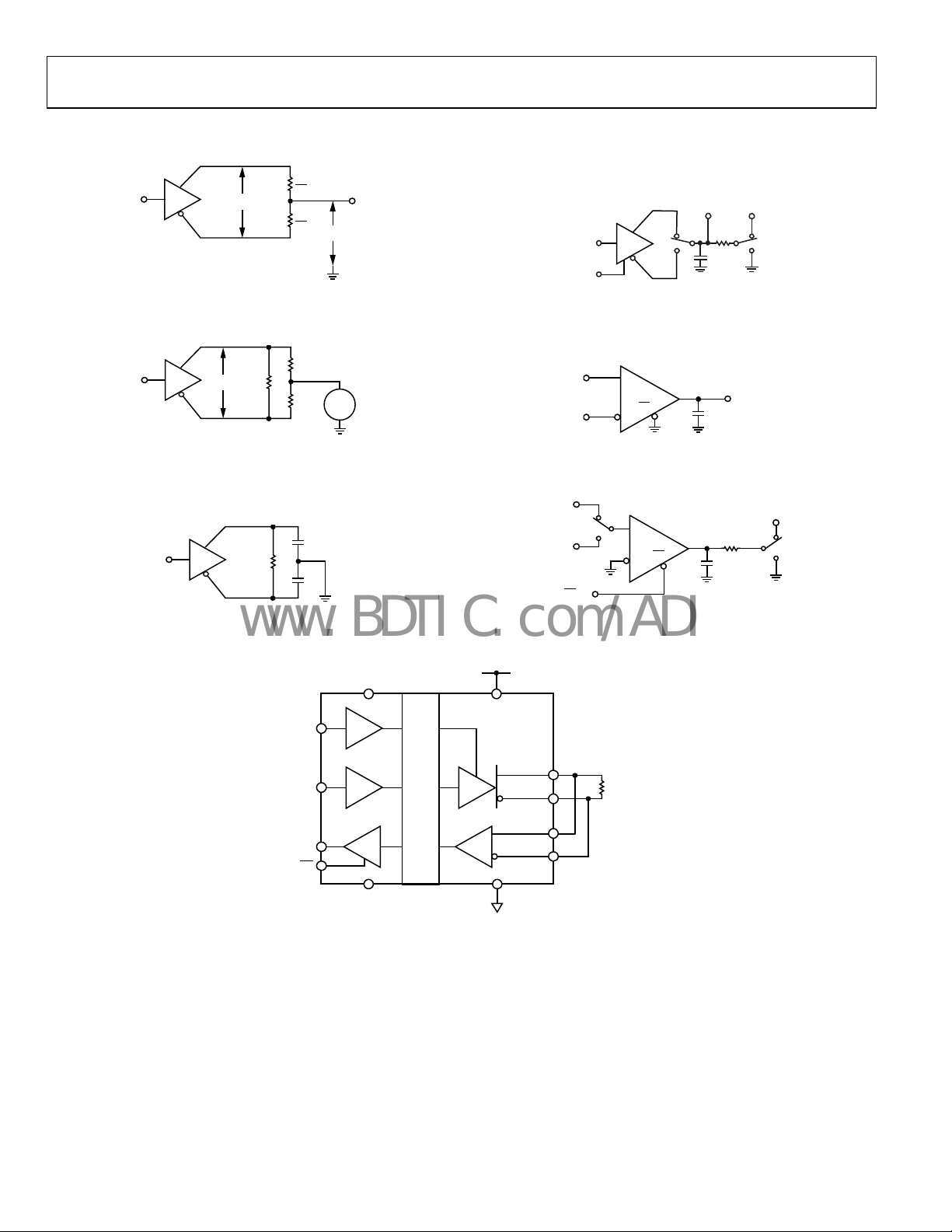
TEST CIRCUITS
Y
xD V
Z
OD2
Figure 2. Driver Voltage Measurement
Y
xD V
Z
OD3
60Ω
Figure 3. Driver Voltage Measurement
Y
xD
R
DIFF
Z
Figure 4. Driver Propagation Delay
R
L
2
R
L
2
375Ω
375Ω
CC
OUT
V
OC
07379-003
TxD
DE
Y
S1 S2
Z
R
110Ω
C
L
50pF
L
07379-007
Figure 5. Driver Enable/Disable
A
V
V
TEST
RE
B
7379-004
OUT
C
L
07379-008
Figure 6. Receiver Propagation Delay
+1.5
C
L
C
L
07379-006
1.5V
RE IN
S1
RE
C
V
L
OUT
V
CC
R
L
S2
07379-009
Figure 7. Receiver Enable/Disable
V
DD1
V
DE
TxD
RxD
RE
GND
GALVANIC ISOLATION
1
Figure 8. Supply-Current Measurement Test Circuit
DD2
DD2
GND
Y
120Ω
Z
A
B
2
07379-005
Rev. 0 | Page 6 of 20

ADM2482E/ADM2487E
V
A
Y
Y
V
www.BDTIC.com/ADI
SWITCHING CHARACTERISTICS
DD1
V
= V
/2V
DD1
t
DPHL
– V
(Y)
90% POINT
(Z)
t
DF
07379-010
DE
0.5V
DD1
t
ZL
2.3V
, Z
t
ZH
2.3V
, Z
t
t
0.5V
LZ
HZ
DD1
VOL+ 0.5V
– 0.5V
V
OH
DD1
0V
V
OL
V
OH
07379-012
0V
Figure 11. Driver Enable/Disable Timing
0.7V
DD1
RE
0.5V
t
ZL
DD1
t
0.5V
LZ
DD1
0.3V
DD1
/2
DD1
0V
Z
V
O
Y
+V
O
V
DIFF
–V
10% POINT 10% POINT
O
1/2V
O
90% POINT
t
DPLH
t
V
DIFF
DR
Figure 9. Driver Propagation Delay, Rise/Fall Timing
–B
0V 0V
1.5V
OUTPUT LOW
t
ZH
OUTPUT HIGH
1.5V
t
HZ
VOL+ 0.5V
V
Figure 12. Receiver Enable/Disable Timing
OH
– 0.5V
V
OL
V
OH
07379-013
RxD
t
PLH
1.5V 1.5V
t
= |
t
PLH
–
SKEW
Figure 10. Receiver Propagation Delay
t
PHL
V
OH
t
|
PHL
V
07379-011
OL
RxD
RxD
0V
Rev. 0 | Page 7 of 20

ADM2482E/ADM2487E
www.BDTIC.com/ADI
ABSOLUTE MAXIMUM RATINGS
All voltages are relative to their respective ground; TA = 25°C,
unless otherwise noted.
Table 6.
Parameter Rating
V
−0.5 V to +6 V
DD1
V
−0.5 V to +6 V
DD2
Digital Input Voltages (DE, RE, TxD)
Digital Output Voltages
RxD −0.5 V to V
D1, D2 13 V
Driver Output/Receiver Input Voltage −9 V to +14 V
Operating Temperature Range −40°C to +85°C
Storage Temperature Range −55°C to +150°C
Average Output Current per Pin −35 mA to +35 mA
ESD (Human Body Model) on A, B, Y
and Z pins
Lead Temperature
Soldering (10 sec) 300°C
Vapor Phase (60 sec) 215°C
Infrared (15 sec) 220°C
−0.5 V to V
±15 kV
+ 0.5 V
DD1
+ 0.5 V
DD1
Stresses above those listed under Absolute Maximum Ratings
may cause permanent damage to the device. This is a stress
rating only; functional operation of the device at these or any
other conditions above those indicated in the operational
section of this specification is not implied. Exposure to absolute
maximum rating conditions for extended periods may affect
device reliability.
ESD CAUTION
Rev. 0 | Page 8 of 20

ADM2482E/ADM2487E
G
e
www.BDTIC.com/ADI
PIN CONFIGURATION AND FUNCTION DESCRIPTIONS
D1
1
2
D2
ADM2482E/
ND
3
1
4
DD1
5
RxD
RE
6
DE
7
TxD
8
NC = NO CONNECT
ADM2487E
TOP VIEW
(Not to Scale)
V
Figure 13. Pin Configuration
Table 7. Pin Function Descriptions
Pin No. Mnemonic Description
1 D1 Transformer Driver Terminal 1.
2 D2 Transformer Driver Terminal 2.
3 GND1 Ground, Logic Side.
4 V
DD1
Power Supply, Logic Side (3.3 V or 5 V). Decoupling capacitor to GND
between 0.01 μF and 0.1 μF.
5 RxD
Receiver Output Data. This output is high when (A – B) > +200 mV and low when (A – B) < –200 mV. The
output is tristated when the receiver is disabled, that is, when RE is driven high.
6
RE
Receiver Enable Input. This is an active-low input. Driving this input low enables the receiver; driving it high
disables the receiver.
7 DE Driver Enable Input. Driving this input high enables the driver; driving it low disables the driver.
8 TxD Transmit Data.
9 GND2 Ground, Bus Side.
10 NC No Connect. This pin must be left floating.
11 Y Driver Noninverting Output.
12 Z Driver Inverting Output.
13 B Receiver Inverting Input.
14 A Receiver Noninverting Input.
15 GND2 Ground, Bus Side.
16 V
DD2
Power Supply, Bus Side (Isolated 3.3 V Supply). Decoupling capacitor to GND
between 0.01 μF and 0.1 μF.
V
16
DD2
15
GND
2
A
14
B
13
12
Z
Y
11
NC
10
GND
9
2
07379-002
required; capacitor value should be
1
required; capacitor value should b
2
Rev. 0 | Page 9 of 20

ADM2482E/ADM2487E
www.BDTIC.com/ADI
TYPICAL PERFORMANCE CHARACTERISTICS
2.30
2.25
2.20
(mA)
DD1
2.15
2.10
2.05
SUPPLY CURRENT I
2.00
NO LOAD
54Ω LOAD
120Ω LOAD
60
50
(mA)
40
DD1
30
20
SUPPLY CURRENT I
10
NO LOAD
54Ω LOAD
120Ω LOAD
1.95
–40 –15 10 35 60 85
Figure 14. ADM2487E I
(Data Rate = 500 kbps, V
40
35
30
(mA)
25
DD2
20
15
10
SUPPLY CURRENT I
5
0
–40 –15 10 35 60 85
Figure 15. ADM2487E I
(Data Rate = 500 kbps, V
4.0
3.9
3.8
(mA)
3.7
DD1
3.6
3.5
3.4
3.3
SUPPLY CURRENT I
3.2
3.1
–40 –15 10 35 60 85
Figure 16. ADM2482E I
16 Mbps, V
TEMPERATURE (° C)
Supply Current vs. Temperature
DD1
= 5 V, V
DD1
TEMPERATURE ( °C)
Supply Current vs. Temperature (See Figure 8)
DD2
TEMPERATURE (° C)
Supply Current vs. Temperature (Data Rate =
DD1
= 5 V, V
DD1
= 3.3 V, DE = 1 V, RE = 0 V)
DD2
= 5 V, V
DD1
= 3.3 V, DE = 1 V, RE = 0 V)
DD2
= 3.3 V, DE = 1 V, RE = 0 V)
DD2
NO LOAD
54Ω LOAD
120Ω LOAD
NO LOAD
54Ω LOAD
120Ω LOAD
0
–40 –15 10 35 60 85
07379-029
TEMPERATURE (° C)
07379-032
Figure 17. ADM2482E Supply Current vs. Temperature (See Figure 8) (Data
Rate = 16 Mbps, V
600
500
400
300
200
100
DRIVER PROPAG ATION DEL AY (ns)
0
–40 –20 0 20 40 60 80
07379-030
= 5 V, V
DD1
DD2
t
DPLH
t
DPHL
TEMPERATURE ( °C)
= 3.3 V, DE = 1, RE =0 V)
07379-033
Figure 18. ADM2487E Driver Propagation Delay vs. Temperature
70
65
60
55
50
45
40
35
30
DRIVER PROPAG ATION DEL AY (ns)
25
20
07379-031
–40 –15 10 35 60 85
Figure 19. ADM2482E Driver Propagation Delay vs. Temperature
t
DPLH
t
DPHL
TEMPERATURE (° C)
07379-034
Rev. 0 | Page 10 of 20

ADM2482E/ADM2487E
www.BDTIC.com/ADI
0
–10
–20
–30
–40
–50
OUTPUT CURRENT ( mA)
–60
–70
012345
OUTPUT VOLTAGE (V)
Figure 20. Output Current vs. Receiver Output High Voltage
60
50
40
30
0.32
0.30
0.28
0.26
0.24
OUTPUT VOLTAGE (V)
0.22
0.20
–40 –20 0 20 40 60 80
07379-016
TEMPERATURE (°C)
07379-019
Figure 23. Receiver Output Low Voltage vs. Temperature
= 4 mA)
(I
DD2
D1
1
20
OUTPUT CURRENT (mA)
10
0
012345
OUTPUT VOLTAGE (V)
Figure 21. Output Current vs. Receiver Output Low Voltage
4.75
4.74
4.73
4.72
4.71
4.70
OUTPUT VOLTAGE (V)
4.69
4.68
4.67
–40 –20 0 20 40 60 80
TEMPERATURE (°C)
Figure 22. Receiver Output High Voltage vs. Temperature
= –4 mA)
(I
DD2
2
07379-017
D2
CH1 2.0V Ω CH2 2.0V Ω M400ns 125MS/s
8.0ns/p t
A CH2 1.52V
07379-020
Figure 24. Switching Waveforms
(50 Ω Pull-Up to V
D1
1
07379-018
D2
CH1 2.0V Ω CH2 2.0V Ω M80ns 625MS /s
on D1 and D2)
DD1
1.6ns/p t
A CH2 1.52V
07379-021
Figure 25. Switching Waveforms
(Break-Before-Make, 50 Ω Pull-Up to V
on D1 and D2)
DD1
Rev. 0 | Page 11 of 20

ADM2482E/ADM2487E
www.BDTIC.com/ADI
T
1
2
4
TxD
Z, B
Y, A
CH1 2.00V CH2 2.00V
CH3 2.00V CH4 2.00V
RxD
M 200ns A CH2 1.72V
T 47.80%
07379-035
Figure 26. ADM2487E Driver/Receiver Propagation Delay, Low to High
= 54 Ω, CL1 = CL2 = 100 pF)
(R
DIFF
T
1
2
TxD
Z, B
Y, A
1
2
4
CH1 2.0V Ω CH2 2.0V Ω
CH3 2.0V Ω CH4 2.0V Ω
TxD
M 40.0ns 1. 25GS/s
A CH2 1.68V
Z, B
Y, A
RxD
IT 16.0ps/pt
07379-037
Figure 28. ADM2482E Driver/Receiver Propagation Delay, High to Low
(R
= 54 Ω, CL1 = CL2 = 100 pF)
DIFF
TxD
1
Z, B
2
Y, A
4
CH1 2.00V CH2 2.00V
CH3 2.00V CH4 2.00V
RxD
M 200ns A CH2 1.72V
T 48.60%
07379-036
Figure 27. ADM2487E Driver/Receiver Propagation Delay, High to Low
= 54 Ω, CL1 = CL2 = 100 pF)
(R
DIFF
4
CH1 2.0V Ω CH2 2.0V Ω
CH3 2.0V Ω CH4 2.0V Ω
RxD
M 40.0ns 1. 25GS/s
A CH2 1.68V
IT 16.0ps/pt
07379-038
Figure 29. ADM2482E Driver/Receiver Propagation Delay, Low to High
(R
= 54 Ω, CL1 = CL2 = 100 pF)
DIFF
Rev. 0 | Page 12 of 20

ADM2482E/ADM2487E
V
V
www.BDTIC.com/ADI
CIRCUIT DESCRIPTION
ELECTRICAL ISOLATION
In the ADM2482E/ADM2487E, electrical isolation is implemented on the logic side of the interface. Therefore, the part has
two main sections: a digital isolation section and a transceiver
section (see Figure 30). Driver input and data enable applied
to the TxD and DE pins, respectively, and referenced to logic
ground (GND
appear at the transceiver section referenced to isolated ground
(GND
). Similarly, the receiver output, referenced to isolated
2
ground in the transceiver section, is coupled across the isolation
barrier to appear at the RxD pin referenced to logic ground.
iCoupler Technology
The digital signals transmit across the isolation barrier using
iCoupler technology. This technique uses chip scale transformer
windings to couple the digital signals magnetically from one
side of the barrier to the other. Digital inputs are encoded into
waveforms that are capable of exciting the primary transformer
winding. At the secondary winding, the induced waveforms are
decoded into the binary value that was originally transmitted.
Positive and negative logic transitions at the input cause narrow
pulses (~1 ns) to be sent to the decoder, via the transformer.
The decoder is bistable and is, therefore, either set or reset by
the pulses, indicating input logic transitions. In the absence of
logic transitions at the input for more than ~1 μs, a periodic set
of refresh pulses indicative of the correct input state are sent to
ensure dc correctness at the output. If the decoder receives no
internal pulses for more than about 5 μs, then the input side is
assumed to be unpowered or nonfunctional, in which case the
output is forced to a default state (see Tab l e 8 ).
DE
) are coupled across an isolation barrier to
1
DD1
D1 D2
OSC
ENCODE DECODE
ISOLATION
BARRIER
DD2
TRUTH TABLES
The truth tables in this section use the abbreviations found in
Tabl e 8.
Table 8. Truth Table Abbreviations
Letter Description
H High level
I Indeterminate
L Low level
X Irrelevant
Z High impedance (off)
NC Disconnected
Table 9. Transmitting
Supply Status Inputs Outputs
V
V
DD1
On On H H H L
On On H L L H
On On L X Z Z
On Off X X Z Z
Off On L X Z Z
Off Off X X Z Z
Table 10. Receiving
Supply Status Inputs Outputs
V
V
DD1
On On >−0.03 V L or NC H
On On <−0.2 V L or NC L
On On −0.2 V < A − B < −0.03 V L or NC I
On On Inputs open L or NC H
On On X H Z
On Off X L or NC H
Off Off X L or NC L
DE TxD Y Z
DD2
A − B
DD2
RxD
RE
TxD
RxD
RE
DIGITAL ISOLATION TRANSCEIVER
Figure 30. ADM2482E/ADM2487E Digital Isolation and Transceiver Sections
ENCODE
ENCODE DECODE
GND
1
DECODE
GND
D
R
2
Y
Z
A
B
07379-022
Rev. 0 | Page 13 of 20

ADM2482E/ADM2487E
www.BDTIC.com/ADI
THERMAL SHUTDOWN
The ADM2482E/ADM2487E contain thermal shutdown
circuitry that protects the part from excessive power dissipation during fault conditions. Shorting the driver outputs to a
low impedance source can result in high driver currents. The
thermal sensing circuitry detects the increase in die temperature
under this condition and disables the driver outputs. This
circuitr y is designed to disable the driver outputs when a die
temperature of 150°C is reached. As the device cools, the drivers
are re-enabled at a temperature of 140°C.
Given the geometry of the receiving coil and an imposed
requirement that the induced voltage is, at most, 50% of the
0.5 V margin at the decoder, a maximum allowable magnetic
field can be determined using Figure 31.
100
10
1
TRUE FAIL-SAFE RECEIVER INPUTS
The receiver inputs have a true fail-safe feature that ensures
that the receiver output is high when the inputs are open or
shorted. During line-idle conditions, when no driver on the
bus is enabled, the voltage across a terminating resistance at
the receiver input decays to 0 V. With traditional transceivers,
receiver input thresholds specified between −200 mV and
+200 mV mean that external bias resistors are required on the
A and B pins to ensure that the receiver outputs are in a known
state. The true fail-safe receiver input feature eliminates the
need for bias resistors by specifying the receiver input threshold
between −30 mV and −200 mV. The guaranteed negative threshold means that when the voltage between A and B decays to
0 V, the receiver output is guaranteed to be high.
MAGNETIC FIELD IMMUNITY
The limitation on the magnetic field immunity of the iCoupler
is set by the condition in which an induced voltage in the
receiving coil of the transformer is large enough to either
falsely set or reset the decoder. The following analysis defines
the conditions under which this may occur. The 3 V operating
condition of the ADM2482E/ADM2487E is examined because
it represents the most susceptible mode of operation.
The pulses at the transformer output have an amplitude greater
than 1 V. The decoder has a sensing threshold of about 0.5 V,
thus establishing a 0.5 V margin in which induced voltages can
be tolerated.
The voltage induced across the receiving coil is given by
−
dβ
⎛
⎞
=
V
⎜
dt
⎝
where:
β is the magnetic flux density (gauss).
N is the number of turns in the receiving coil.
r
is the radius of the nth turn in the receiving coil (cm).
n
2
⎟
∑
n
⎠
Nnr
,,2,1;
K=π
0.1
FLUX DENSITY (kGAUSS)
0.01
MAXIMUM ALLOWABLE MAG NETIC
0.001
1k 10k 100k 100M1M 10M
Figure 31. Maximum Allowable External Magnetic Flux Density
MAGNETIC FIELD FREQUENCY (Hz)
07379-023
For example, at a magnetic field frequency of 1 MHz, the
maximum allowable magnetic field of 0.2 kgauss induces a
voltage of 0.25 V at the receiving coil. This is about 50% of the
sensing threshold and does not cause a faulty output transition.
Similarly, if such an event occurs during a transmitted pulse and
is the worst-case polarity, it reduces the received pulse from
>1.0 V to 0.75 V, still well above the 0.5 V sensing threshold
of the decoder.
Figure 32 shows the magnetic flux density values in terms of
more familiar quantities, such as maximum allowable current
flow at given distances away from the ADM2482E/ADM2487E
transformers.
1000
DISTANCE = 1m
100
DISTANCE = 5mm
10
1
0.1
MAXIMUM ALL OWABLE CURRENT ( kA)
0.01
DISTANCE = 100mm
1k 10k 100k 100M1M 10M
MAGNETIC FIELD FREQUENCY (Hz)
Figure 32. Maximum Allowable Current for
Various Current-to-ADM2482E/ADM2487E Spacings
07379-024
With combinations of strong magnetic field and high frequency,
any loops formed by PCB traces could induce error voltages
large enough to trigger the thresholds of succeeding circuitry.
Care should be taken in the layout of such traces to avoid this
possibility.
Rev. 0 | Page 14 of 20

ADM2482E/ADM2487E
L
A
F
www.BDTIC.com/ADI
APPLICATIONS INFORMATION
PRINTED CIRCUIT BOARD LAYOUT
The isolated RS-485 transceiver of the ADM2482E/ADM2487E
requires no external interface circuitry for the logic interfaces.
Power supply bypassing is required at the input and output supply
pins (see Figure 33).
Bypass capacitors are most conveniently connected between
Pin 3 and Pin 4 for V
. The capacitor value must be between 0.01 μF and 0.1 μF.
V
DD2
and between Pin 15 and Pin 16 for
DD1
The total lead length between both ends of the capacitor and
the input power supply pin must not exceed 20 mm.
Bypassing Pin 9 and Pin 16 is also recommended unless the
ground pair on each package side is connected close to the
package.
D1
GND
V
RxD
TxD
D2
1
DD1
RE
DE
ADM2482E
OR
ADM2487E
TOP VIEW
(Not to Scale)
NC = NO CONNECT
Figure 33. Recommended Printed Circuit Board Layout
V
DD2
GND
A
B
Z
Y
NC
GND
2
2
07379-025
In applications involving high common-mode transients, care
must be taken to ensure that board coupling across the isolation
barrier is minimized. Furthermore, the board layout must be
designed such that any coupling that does occur equally affects
all pins on a given component side.
Failure to ensure this can cause voltage differentials between
pins exceeding the absolute maximum ratings of the device,
thereby leading to latch-up or permanent damage.
ISOLATED POWER SUPPLY CIRCUIT
The ADM2482E/ADM2487E integrate a transformer driver
that, when used with an external transformer and linear voltage
regulator (LDO), generates an isolated 3.3 V power supply to be
supplied between V
and GND2, as shown in Figure 34.
DD2
Pin D1 and Pin D2 of the ADM2482E/ADM2487E drive a
center-tapped Transformer T1. A pair of Schottky diodes and a
smoothing capacitor are used to create a rectified signal from the
secondary winding. The ADP1710 LDO provides a regulated
3.3 V power supply to the ADM2482E/ ADM2487E bus-side
circuitry (V
DD2
).
When the ADM2482E/ADM2487E are powered by 3.3 V on the
logic side, a step-up transformer is required to compensate for
the forward voltage drop of the Schottky diodes and the voltage
drop across the regulator. The transformer turns ratio should be
chosen to ensure just enough headroom for the ADP1710 LDO
to output a regulated 3.3 V output under all operating
conditions.
If the ADM2482E/ADM2487E are powered by 5 V on the
logic side, then a step-down transformer should be used.
For optimum efficiency, the transformer turns ratio should
be chosen to ensure just enough headroom for the ADP1710
LDO to output a regulated 3.3 V output under all operating
conditions.
ISO
TION
100n
V
CC
V
D1 D2
DD1
ADM2482E/
ADM2487E
GND
1
BARRIER
1N5817
V
10µF
MLC
CC
T1
1N5817
V
GND
DD2
2
22µF
ISOLATED 3.3V
100nF
Figure 34. Applications Diagram
LDO
OUT
IN
ADP1710
EN
GND
3.3V
10µF
07379-026
Rev. 0 | Page 15 of 20

ADM2482E/ADM2487E
www.BDTIC.com/ADI
TYPICAL APPLICATIONS
Figure 35 and Figure 36 show typical applications of the
ADM2482E/ADM2487E in half-duplex and full-duplex
RS-485 network configurations. Up to 256 transceivers can
be connected to the RS-485 bus. To minimize reflections, the
MAXIMUM NUMBER OF TRANSCEIVERS ON BUS = 256
ADM2482E/
RxD
RE
DE
TxD
ADM2487E
R
D
A
B
R
T
Z
Y
line must be terminated at the receiving end in its characteristic
impedance, and stub lengths off the main line must be kept as
short as possible. For half-duplex operation, this means that both
ends of the line must be terminated, because either end can be
the receiving end.
ADM2482E/
ADM2487E
A
B
R
T
Z
Y
ABZYABZY
R
RxD
RE
DE
TxD
D
ADM2482E/
ADM2487E
NOTES
1. R
IS EQUAL TO THE CHARACTERI STIC IM PEDANCE OF THE CABLE.
T
2. ISOLATION NOT SHOWN.
R
D
ADM2482E/
ADM2487E
R
RxD RE DE TxDRxD RE DE TxD
D
07379-027
Figure 35. ADM2482E/ADM2487E Typical Half-Duplex RS-485 Network
RxD
RE
DE
TxD
MASTER
R
D
ADM2482E/
ADM2487E
A
R
T
B
Z
Y
ADM2482E/
ADM2487E
MAXIMUM NUMBER OF NODES = 256
A B Z Y
R
D
A B Z Y
R
D
SLAVESLAVE
ADM2482E/
ADM2487E
RxD RE DE T xD
NOTES
1. R
IS EQUAL TO THE CHARACTERISTIC IM PEDANCE OF THE CABLE.
T
RxD RE DE T xD
Figure 36. ADM2482E/ADM2487E Typical Full-Duplex RS-485 Network
R
T
Y
Z
B
A
SLAVE
D
R
ADM2482E/
ADM2487E
TxD
DE
RE
RxD
07379-028
Rev. 0 | Page 16 of 20

ADM2482E/ADM2487E
C
www.BDTIC.com/ADI
OUTLINE DIMENSIONS
10.50 (0.4134)
10.10 (0.3976)
BSC
9
7.60 (0.2992)
7.40 (0.2913)
8
10.65 (0.4193)
10.00 (0.3937)
2.65 (0.1043)
2.35 (0.0925)
SEATING
PLANE
Wide Body
(RW-16)
8°
0°
0.33 (0.0130)
0.20 (0.0079)
0
0
.
7
.
2
5
(
0
5
(
0
.
0
2
9
5
)
0
0
9
8
)
.
1.27 (0.0500)
0.40 (0.0157)
45°
032707-B
16
1
1.27 (0.0500)
0.30 (0.0 118)
0.10 (0.0039)
OPLANARITY
0.10
CONTROLL ING DIMENS IONS ARE IN MILLIM ETERS; INCH DI MENSIONS
(IN PARENTHESES) ARE ROUNDED-O FF MIL LIMETE R EQUIVALENTS FOR
REFERENCE ONLY AND ARE NOT APPROPRI ATE FOR USE IN DESIGN.
0.51 (0.0201)
0.31 (0.0122)
COMPLIANT TO JEDEC STANDARDS MS-013- AA
Figure 37. 16-Lead Standard Small Outline Package [SOIC_W]
Dimensions shown in millimeters and (inches)
ORDERING GUIDE
Model Data Rate (Mbps) Temperature Range Package Description Package Option
ADM2482EBRWZ
ADM2482EBRWZ-REEL7
ADM2487EBRWZ
ADM2487EBRWZ-REEL7
1
Z = RoHS Compliant Part.
1
1
16 −40°C to +85°C 16-Lead SOIC_W RW-16
1
0.5 −40°C to +85°C 16-Lead SOIC_W RW-16
1
0.5 −40°C to +85°C 16-Lead SOIC_W RW-16
16 −40°C to +85°C 16-Lead SOIC_W RW-16
Rev. 0 | Page 17 of 20

ADM2482E/ADM2487E
www.BDTIC.com/ADI
NOTES
Rev. 0 | Page 18 of 20

ADM2482E/ADM2487E
www.BDTIC.com/ADI
NOTES
Rev. 0 | Page 19 of 20

ADM2482E/ADM2487E
www.BDTIC.com/ADI
NOTES
©2008 Analog Devices, Inc. All rights reserved. Trademarks and
registered trademarks are the property of their respective owners.
D07379-0-5/08(0)
Rev. 0 | Page 20 of 20
 Loading...