Analog Devices ADM242AR, ADM242AN, ADM222AR, ADM222AN, ADM222AARW Datasheet
...
REV. A
Information furnished by Analog Devices is believed to be accurate and
reliable. However, no responsibility is assumed by Analog Devices for its
use, nor for any infringements of patents or other rights of third parties
which may result from its use. No license is granted by implication or
otherwise under any patent or patent rights of Analog Devices.
a
ADM222/ADM232A/ADM242*
One Technology Way, P.O. Box 9106, Norwood, MA 02062-9106, U.S.A.
Tel: 781/329-4700 World Wide Web Site: http://www.analog.com
Fax: 781/326-8703 © Analog Devices, Inc., 2001
High-Speed, 5 V, 0.1 F
CMOS RS-232 Drivers/Receivers
FEATURES
200 kB/s Transmission Rate
Small (0.1 F) Charge Pump Capacitors
Single 5 V Power Supply
Meets All EIA-232-E and V.28 Specifications
Two Drivers and Two Receivers
On-Board DC-DC Converters
9 V Output Swing with 5 V Supply
30 V Receiver Input Levels
Pin Compatible with MAX222/MAX232A/MAX242
APPLICATIONS
Computers
Peripherals
Modems
Printers
Instruments
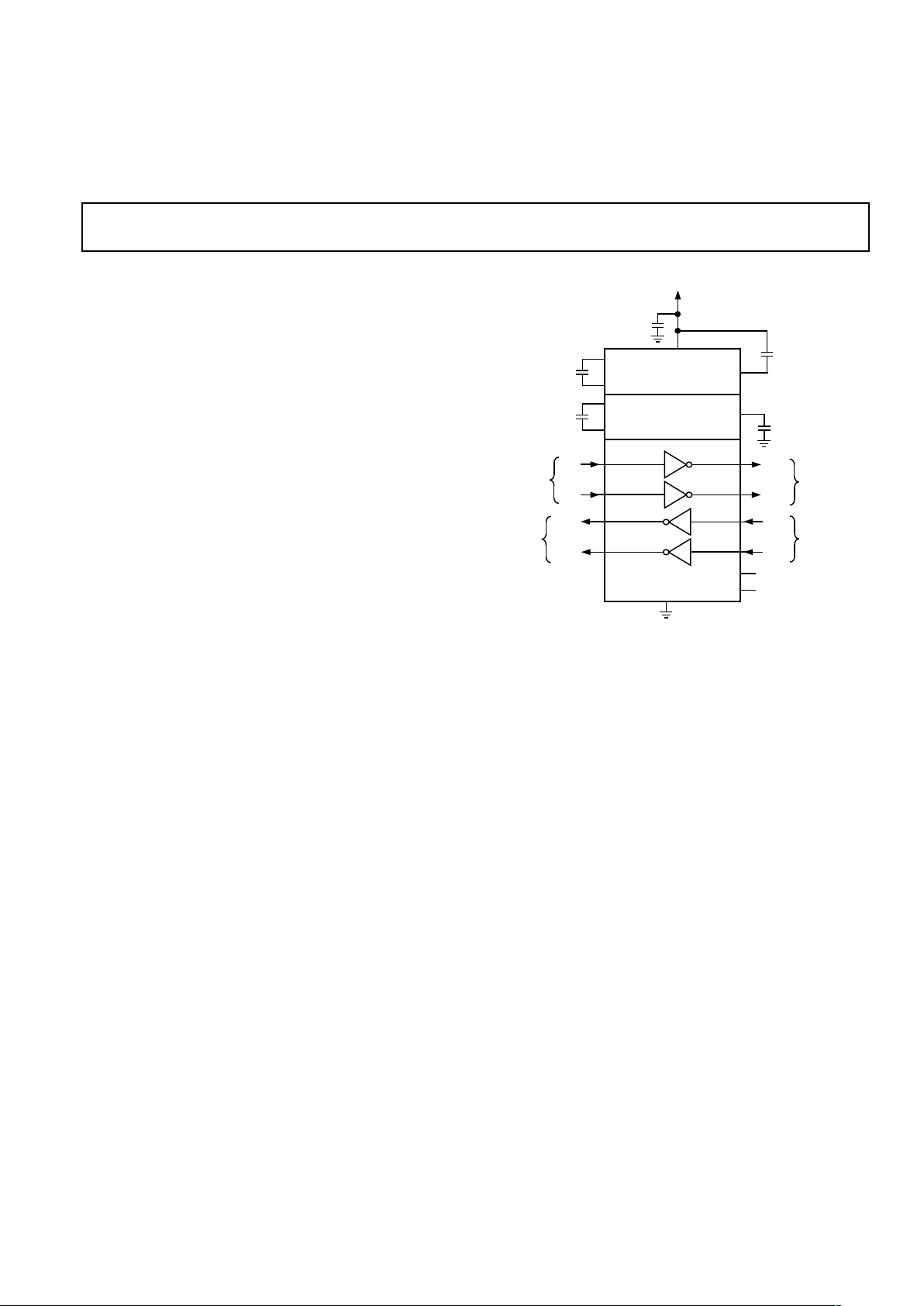
FUNCTIONAL BLOCK DIAGRAM
*
INTERNAL 400k PULL-UP RESISTOR
ON EACH TTL/CMOS INPUT
**
INTERNAL 5k PULL-DOWN RESISTOR
ON EACH RS-232 INPUT
+5V TO +10V
VOLTAGE DOUBLER
+5V TO –10V
VOLTAGE INVERTER
C1+
C1–
V+
V–
C2+
C2–
T1
ADM2xx
T2
R1
R2
0.1F
0.1F
0.1F
GND
TTL/CMOS
OUTPUTS
R1
OUT
R2
OUT
T1
OUT
T2
OUT
R1
IN
R2
IN
T1
IN
T2
IN
TTL/CMOS
INPUTS
*
RS-232
OUTPUTS
RS-232
INPUTS
**
0.1F
5V INPUT
0.1F
EN
SHDN
(ADM242)
(ADM222, ADM242)
V
CC
GENERAL DESCRIPTION
The ADM222, ADM232A, ADM242 are a family of high-speed
RS-232 line drivers/receivers offering transmission rates up to
200 kB/s. Operating from a single 5 V power supply, a highly
efficient on-chip charge pump using small (0.1 µF) external
capacitors allows RS-232 bipolar levels to be developed. Two
RS-232 drivers and two RS-232 receivers are provided on
each device.
The devices are fabricated on BiCMOS, an advanced mixed
technology process that combines low power CMOS with highspeed bipolar circuitry. This allows for transmission rates up to
200 kB/s, yet minimizes the quiescent power supply current to
under 5 mA.
The ADM232A is a pin-compatible, high-speed upgrade for the
AD232 and for the ADM232L. It is available in 16-lead DIP
and in both narrow and wide surface-mount (SOIC) packages.
The ADM222 contains an additional shutdown (SHDN) function that may be used to disable the device, thereby reducing the
supply current to 0.1 µA. During shutdown, all transmit/receive
*Protected by U.S. Patent No. 5,237,209.
functions are disabled. The ADM222 is available in 18-lead
DIP and in a wide surface-mount (SOIC) package.
The ADM242 combines both shutdown (SHDN) and enable
(EN) functions. The shutdown function reduces the supply
current to 0.1 mA. During shutdown, the transmitters are disabled but the receivers continue to operate normally. The
enable function allows the receiver outputs to be disabled
thereby facilitating sharing a common bus. The ADM242 is
available in 18-lead DIP and in a wide surface-mount (SOIC)
package.

REV. A
–2–
ADM222/ADM232A/ADM242–SPECIFICATIONS
(VCC = 5 V 10%. C1–C4 = 0.1 F; all specifications T
MIN
to T
MAX
unless otherwise noted.)
Parameter Min Typ Max Unit Test Conditions/Comments
RS-232 TRANSMITTERS
Output Voltage Swing ± 5 ± 9 V All Transmitter Outputs Loaded with
3 kΩ to Ground
Input Logic Threshold Low, V
INL
1.7 0.8 V T
IN
Input Logic Threshold High, V
INH
2.4 1.7 V T
IN
Logic Pull-Up Current 12 40 µAT
IN
= 0 V
Data Rate 200 kB/s
Output Resistance 300 Ω V
CC
= V+ = V– = 0 V, V
OUT
= ± 2 V
Output Short Circuit Current (Instantaneous) ± 10 mA
RS-232 RECEIVERS
RS-232 Input Voltage Range –30 +30 V
RS-232 Input Threshold Low 0.8 1.2 V
RS-232 Input Threshold High 1.6 2.4 V
RS-232 Input Hysteresis 0.2 0.4 1.0 V V
CC
= 5 V
RS-232 Input Resistance 3 5 7 kΩ T
A
= 0°C to 85°C
TTL/CMOS Output Voltage Low, V
OL
0.05 0.4 V I
OUT
= 3.2 mA
TTL/CMOS Output Voltage High, V
OH
3.5 V I
OUT
= –1.0 mA
TTL/CMOS Output Short-Circuit Current –2 –85 mA Source Current (V
OUT
= GND)*
TTL/CMOS Output Short-Circuit Current 10 35 mA Sink Current (V
OUT
= VCC)*
TTL/CMOS Output Leakage Current ± 0.05 ± 10 µA SHDN = GND/EN = V
CC
0 V ≤ V
OUT
≤ V
CC
EN Input Threshold Low, V
INL
1.4 0.8 V
EN Input Threshold High, V
INH
2.0 1.4 V
POWER SUPPLY
Power Supply Current 4 8 mA No Load
13 mA 3 kΩ Load on Both Outputs
Shutdown Power Supply Current 0.1 10 µA
SHDN Input Leakage Current ± 1 µA
SHDN Input Threshold Low, V
INL
1.4 0.8 V
SHDN Input Threshold High, V
INH
2.0 1.4 V
AC CHARACTERISTICS
Transition Region Slew Rate 3 8 30 V/µsCL = 50 pF to 1000 pF, RL = 3 kΩ to 7 kΩ
Measured from +3 V to –3 V or –3 V to +3 V
Transmitter Propagation Delay TTL to RS-232 0.85 3.5 µst
PHLT
1.0 3.5 µst
PLHT
Receiver Propagation Delay RS-232 to TTL 0.1 0.5 µst
PHLR
0.3 0.5 µst
PLHR
Receiver Output Enable Time 125 500 ns t
ER
Receiver Output Disable Time 160 500 ns t
DR
Transmitter Output Enable Time 250 µs SHDN Goes High
Transmitter Output Disable Time 3.5 µs SHDN Goes Low
Transmitter + to – Propagation Delay Difference 150 ns
Receiver + to – Propagation Delay Difference 200 ns
*Guaranteed by design, not production tested.
Specifications subject to change without notice.

REV. A
ADM222/ADM232A/ADM242
–3–
ABSOLUTE MAXIMUM RATINGS*
(TA = 25°C unless otherwise noted)
VCC . . . . . . . . . . . . . . . . . . . . . . . . . . . . . . . . . . . . . . . . . . 6 V
V+ . . . . . . . . . . . . . . . . . . . . . . . . . . . (V
CC
– 0.3 V) to +13 V
V– . . . . . . . . . . . . . . . . . . . . . . . . . . . . . . . . . +0.3 V to –13 V
Input Voltages
T
IN
. . . . . . . . . . . . . . . . . . . . . . . . –0.3 V to (VCC + 0.3 V)
R
IN
. . . . . . . . . . . . . . . . . . . . . . . . . . . . . . . . . . . . . ± 30 V
Output Voltages
T
OUT
. . . . . . . . . . . . . . . . . . . (V+, +0.3 V) to (V–, –0.3 V)
R
OUT
. . . . . . . . . . . . . . . . . . . . . . . –0.3 V to (VCC + 0.3 V)
Short Circuit Duration
T
OUT
. . . . . . . . . . . . . . . . . . . . . . . . . . . . . . . . Continuous
Power Dissipation N-16 . . . . . . . . . . . . . . . . . . . . . . 400 mW
(Derate 7.5 mW/°C above 70°C)
θ
JA
, Thermal Impedance . . . . . . . . . . . . . . . . . . . . 80°C/W
Power Dissipation R-16N . . . . . . . . . . . . . . . . . . . . . 400 mW
(Derate 7 mW/°C above 70°C)
θ
JA
, Thermal Impedance . . . . . . . . . . . . . . . . . . . . 80°C/W
Power Dissipation R-16W . . . . . . . . . . . . . . . . . . . . . 400 mW
(Derate 7 mW/°C above 70°C)
θ
JA
, Thermal Impedance . . . . . . . . . . . . . . . . . . . . 80°CW
Power Dissipation N-18 . . . . . . . . . . . . . . . . . . . . . . 400 mW
(Derate 7 mW/°C above 70°C)
θ
JA
, Thermal Impedance . . . . . . . . . . . . . . . . . . . . 80°C/W
Power Dissipation R-18W . . . . . . . . . . . . . . . . . . . . . 400 mW
(Derate 7 mW/°C above 70°C)
θ
JA
, Thermal Impedance . . . . . . . . . . . . . . . . . . . . 80°C/W
Operating Temperature Range
Industrial (A Version) . . . . . . . . . . . . . . . –40°C to +85°C
Storage Temperature Range . . . . . . . . . . . . –65°C to +150°C
Lead Temperature (Soldering, 10 sec) . . . . . . . . . . . . 300°C
Vapor Phase (60 sec) . . . . . . . . . . . . . . . . . . . . . . . . 215°C
Infrared (15 sec) . . . . . . . . . . . . . . . . . . . . . . . . . . . . . 220°C
*This is a stress rating only and functional operation of the device at these or any
other conditions above those indicated in the operation sections of this specification is not implied. Exposure to absolute maximum rating conditions for extended
periods of time may affect reliability.
ORDERING GUIDE
Temperature Package Package
Model Range Description Option
ADM222AN –40°C to +85°C Plastic DIP N-18
ADM222AR –40°C to +85°C Wide SOIC R-18W
ADM232AAN –40°C to +85°C Plastic DIP N-16
ADM232AARN –40°C to +85°C Narrow SOIC R-16N
ADM232AARW –40°C to +85°C Wide SOIC R-16W
ADM242AN –40°C to +85°C Plastic DIP N-18
ADM242AR –40°C to +85°C Wide SOIC R-18W
Test Circuits
V–
V+
0V
V
OUT
3V
V
IN
t
PHLT
t
PLHT
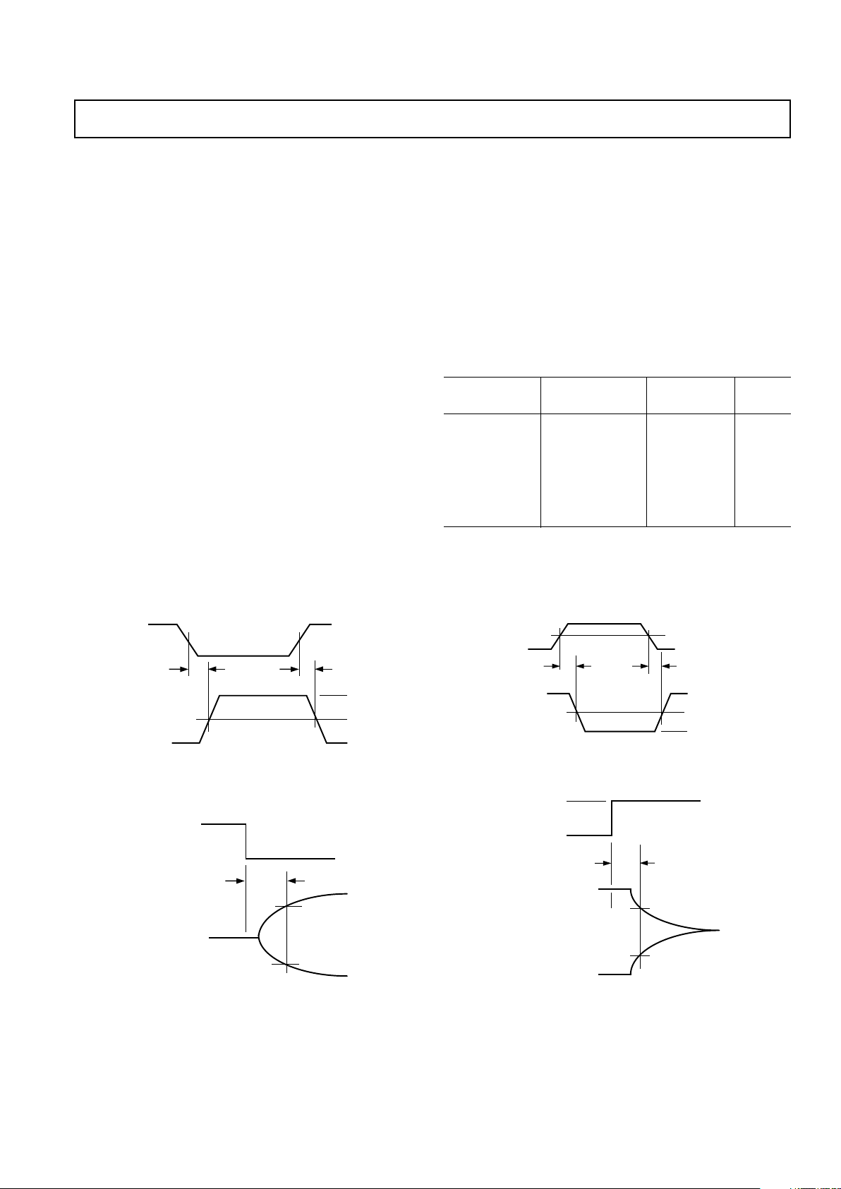
Figure 1. Transmitter Propagation Delay Timing
0.8V
3V
3.5V
RECEIVER
OUTPUT
EN
INPUT
0V
t
ER
Figure 2. Receiver Enable Timing
t
PHLR
t
PLHR
GND
V
CC
50%
V
IN
V
OUT
3V
0V
Figure 3. Receiver Propagation Delay Timing
V
OH
– 0.5V
RECEIVER
OUTPUT
EN
INPUT
VOL + 0.5V
V
OH
V
OL
0V
3V
t
DR
Figure 4. Receiver Disable Timing
 Loading...